
The Study of the Transient Dose Rate Effect on ROIC Pixels in Ultra-Large-Scale Infrared Detectors

Abstract
1. Introduction
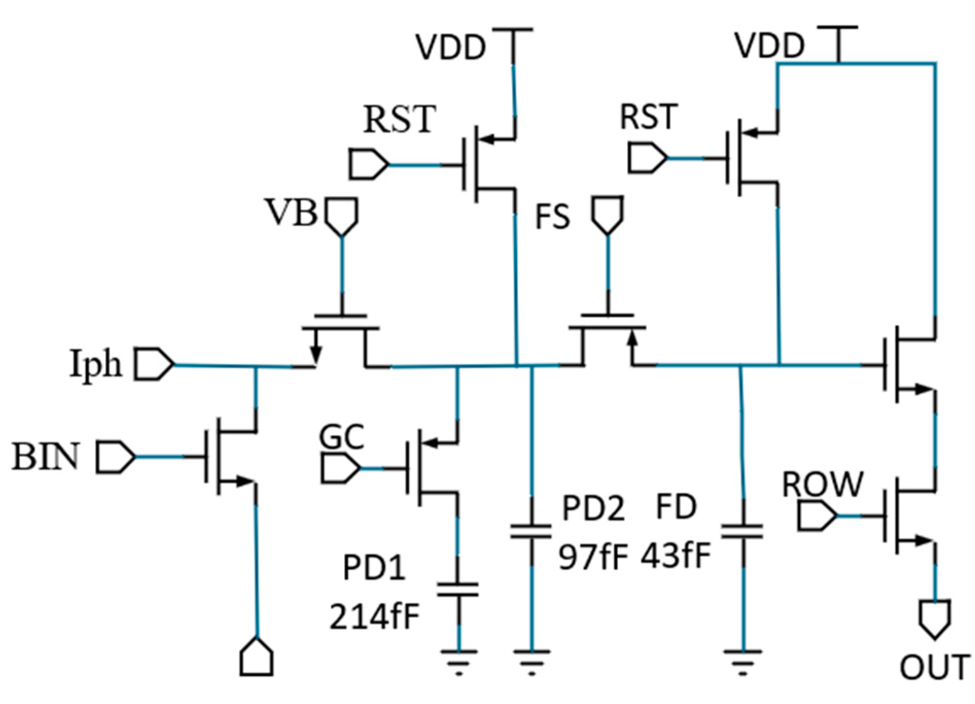
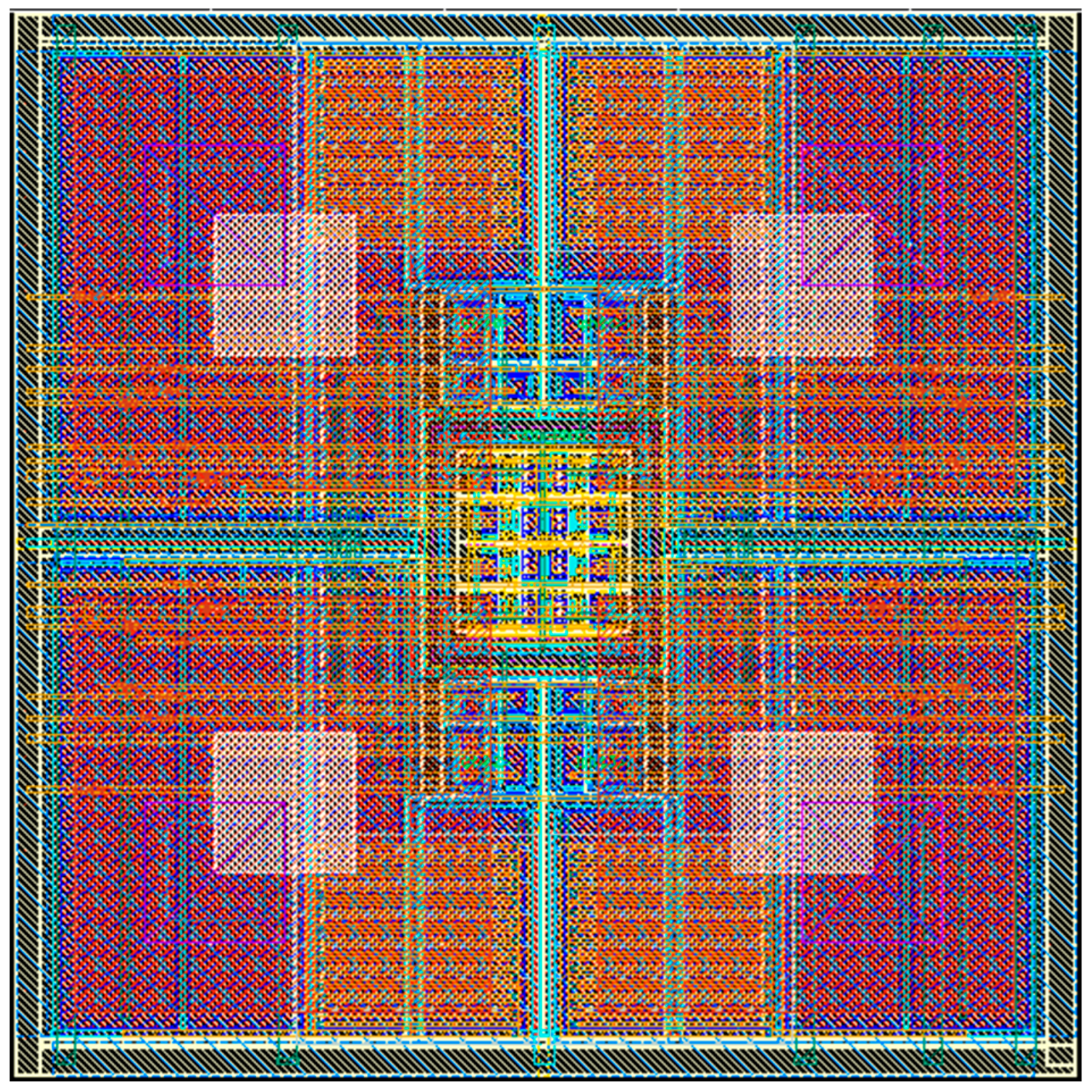
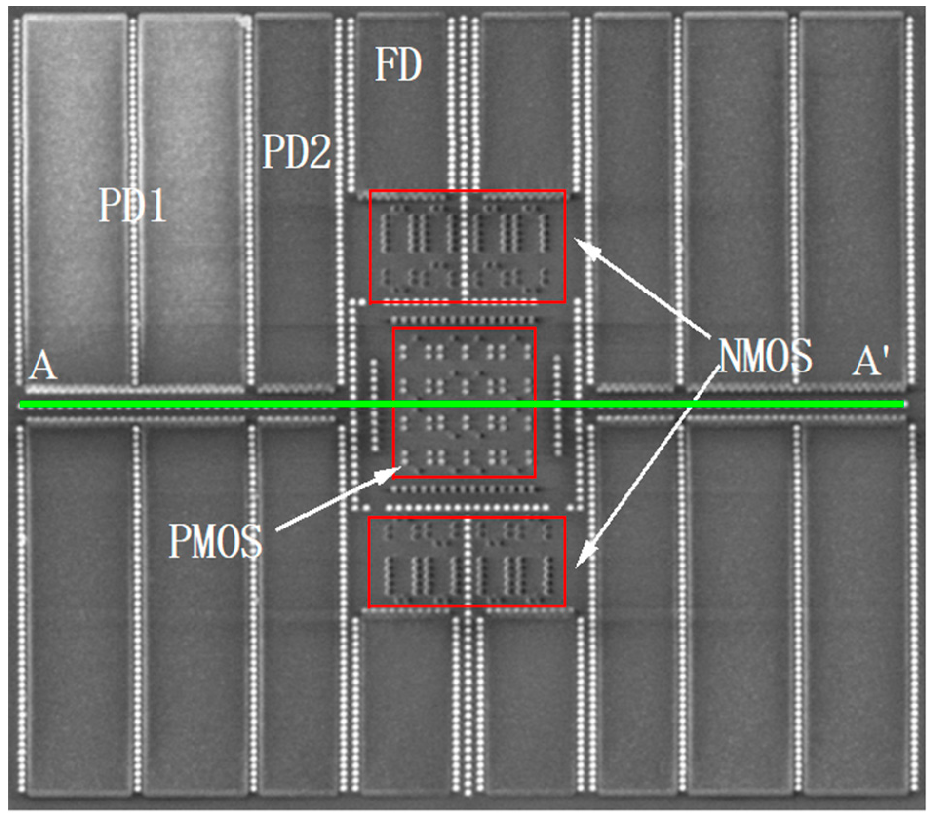
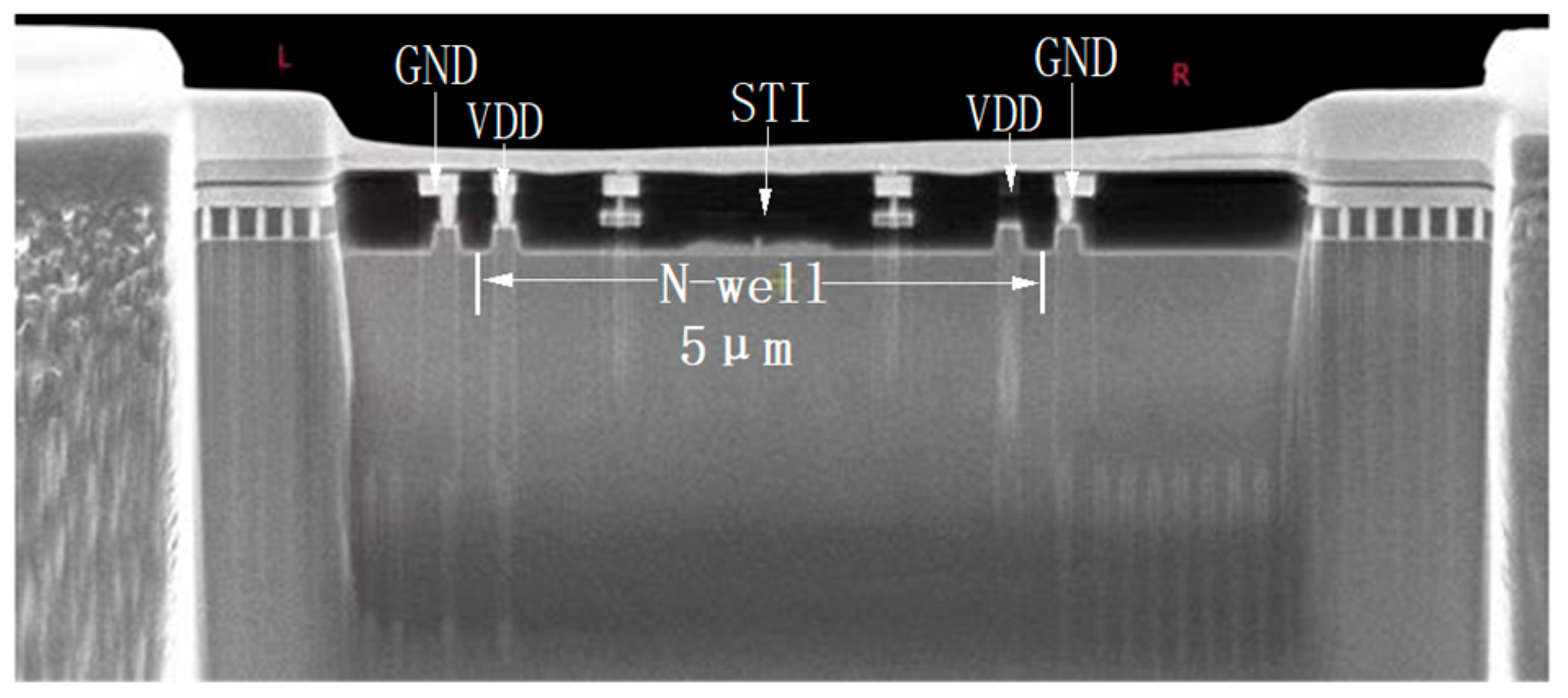
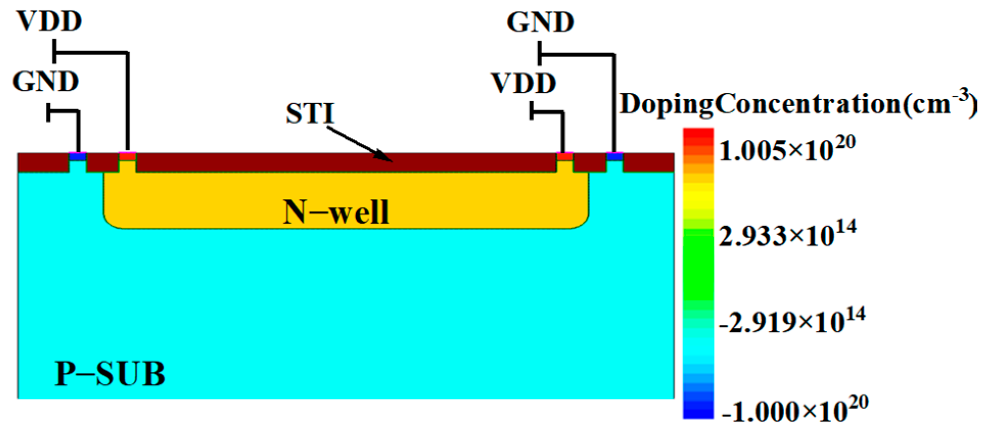
2. Simulation Details
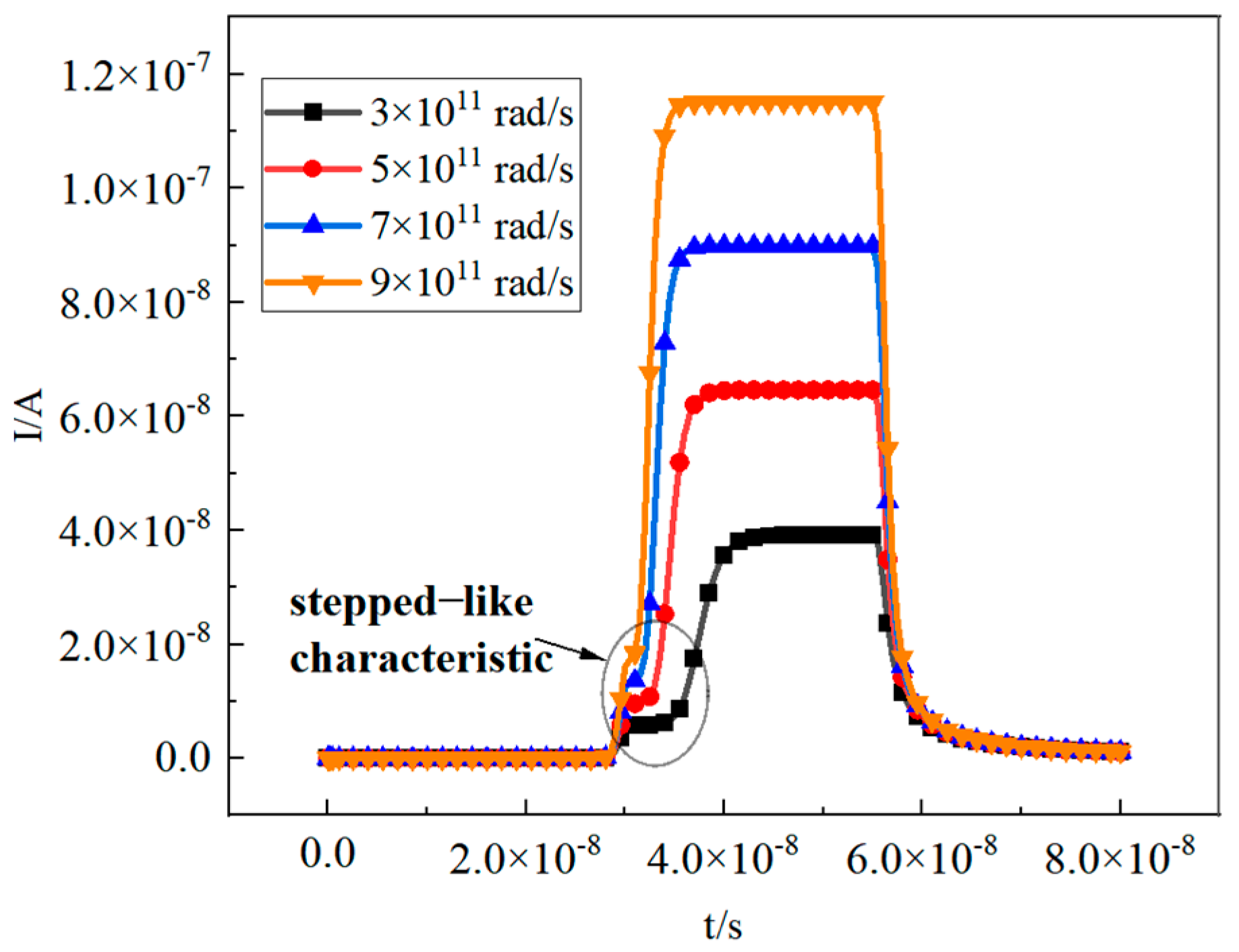
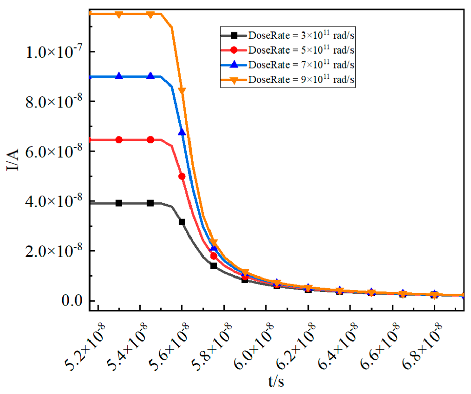
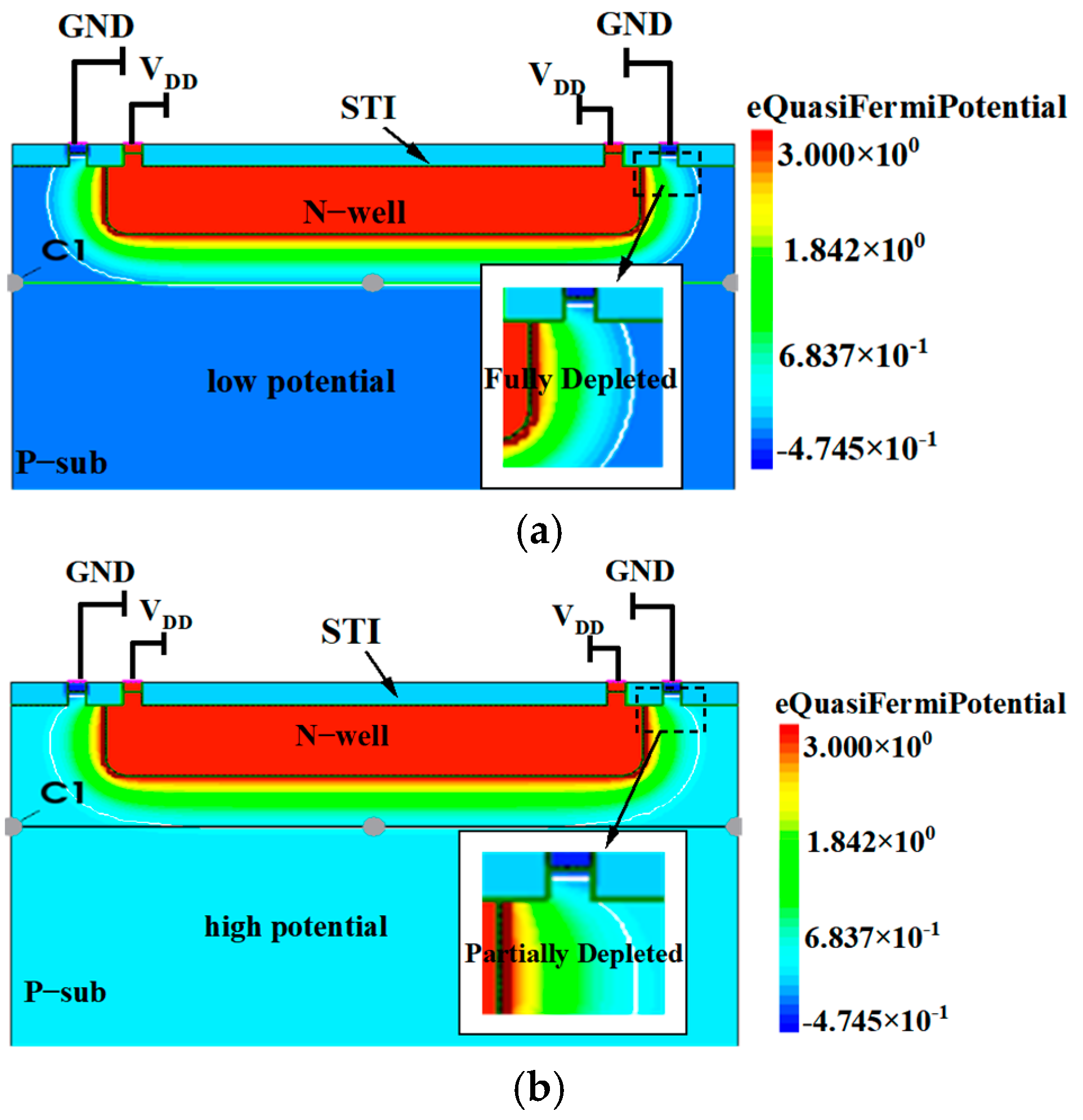
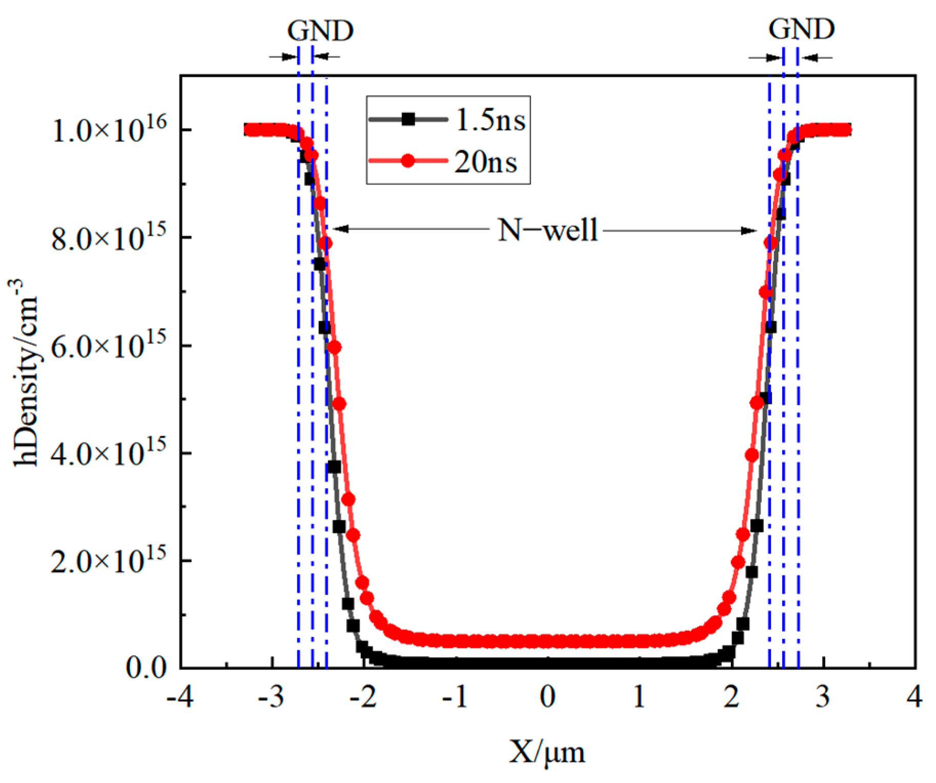
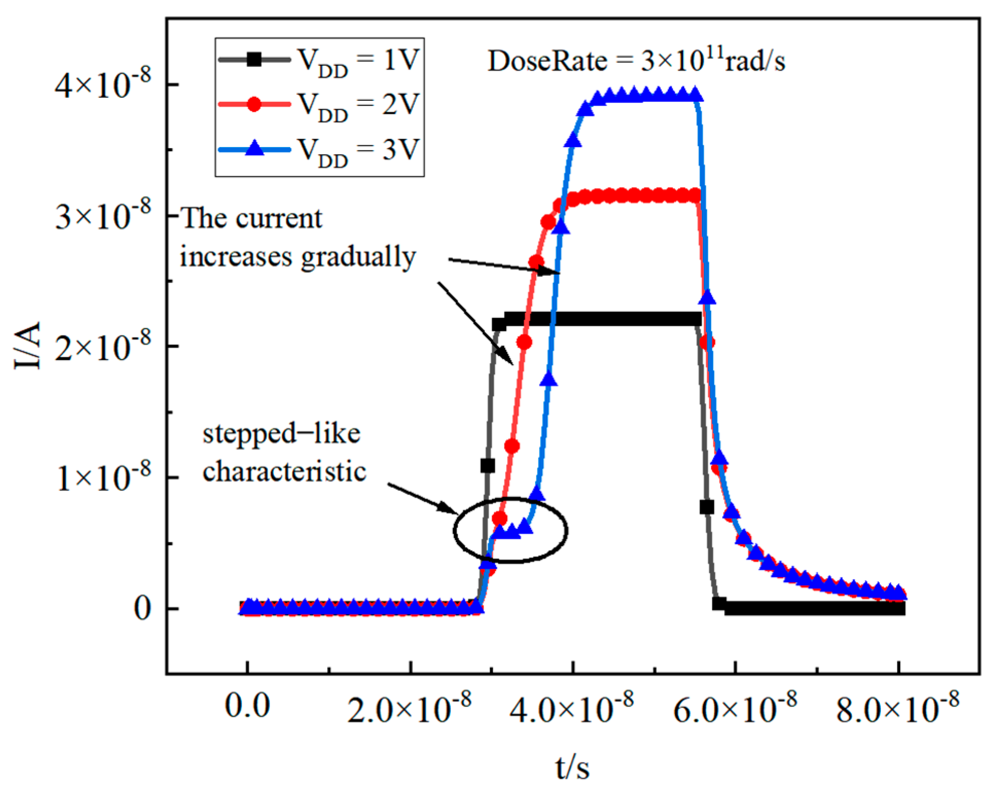
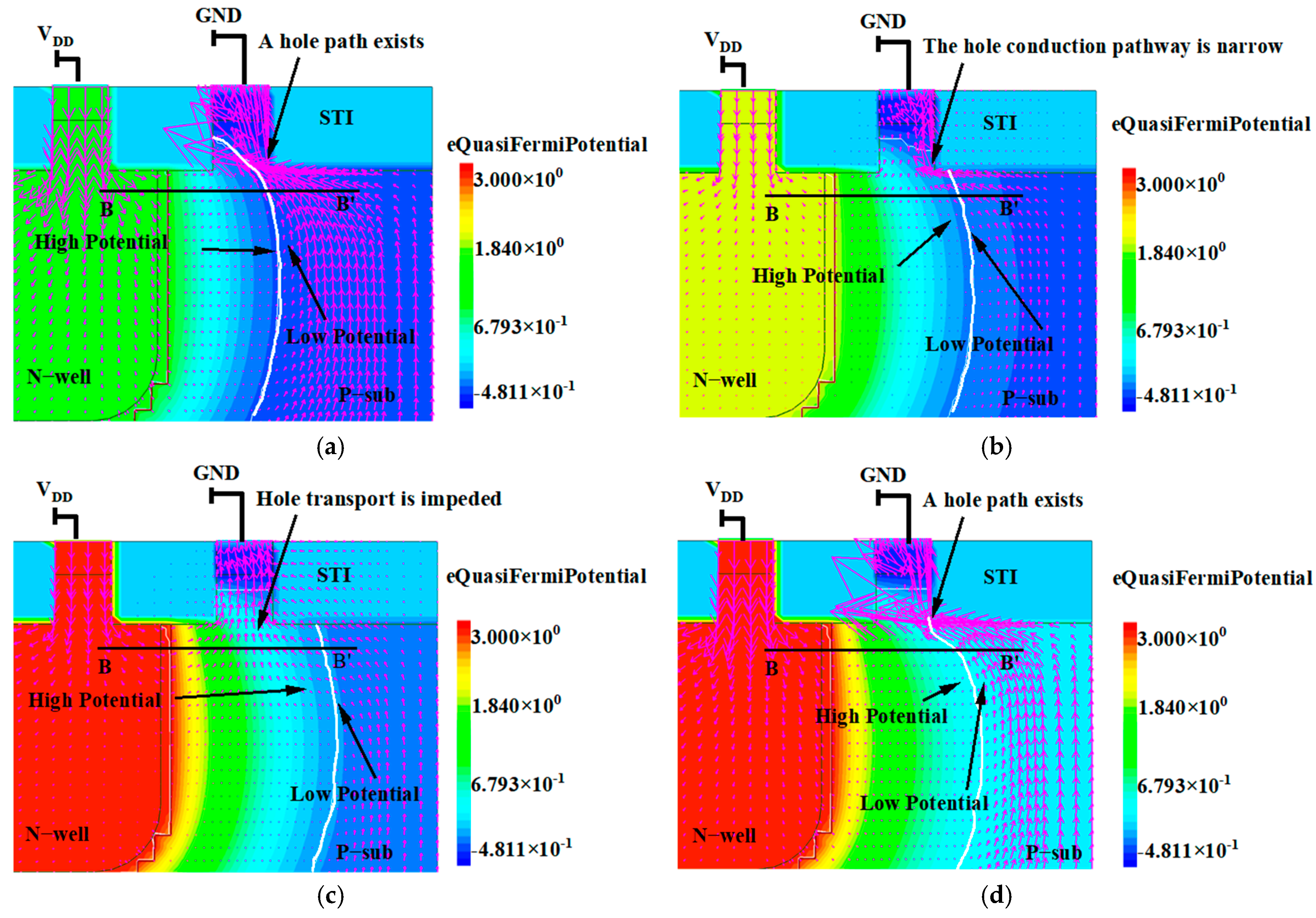
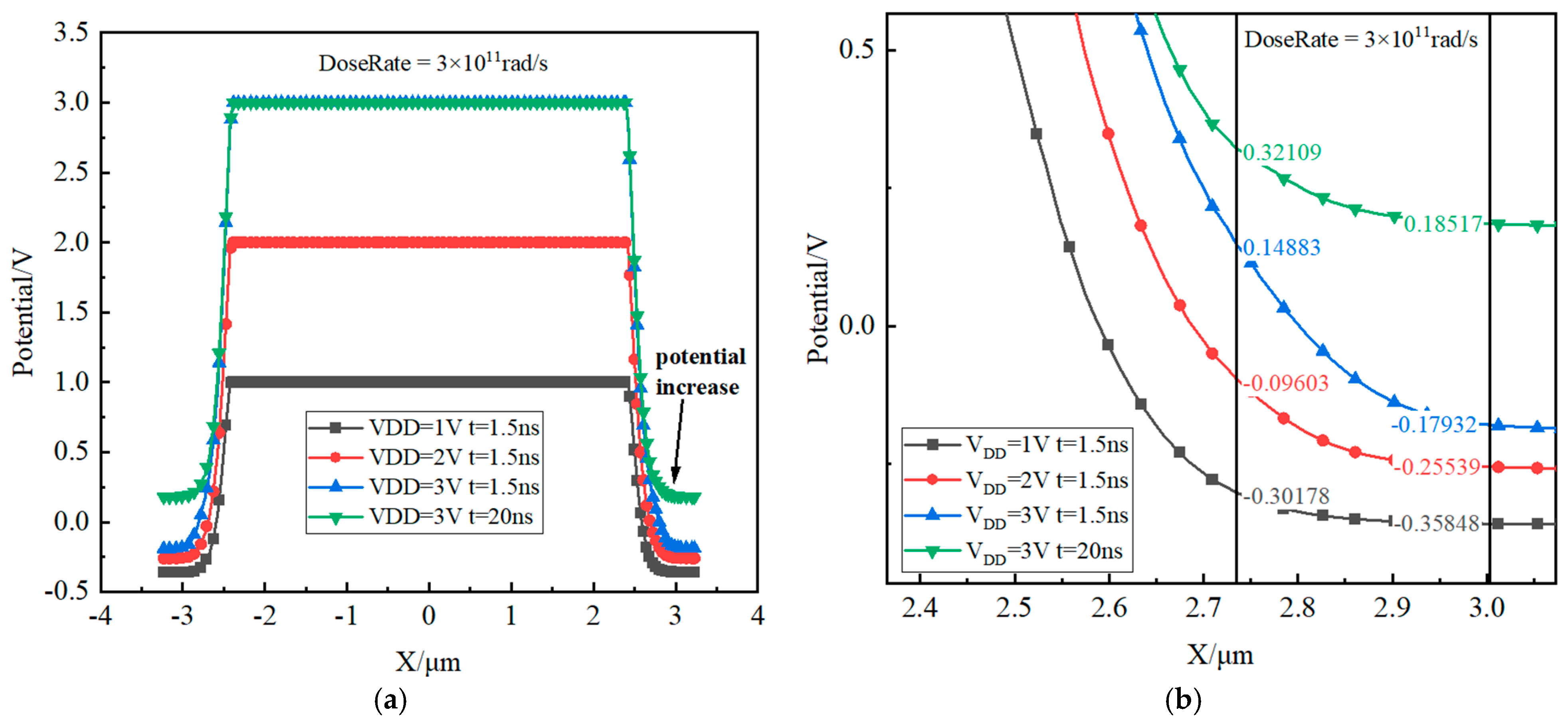
3. Simulation Results and Discussion
4. Conclusions
Author Contributions
Funding
Data Availability Statement
Acknowledgments
Conflicts of Interest
References
- Cai, X. Nuclear Explosion Effects and Protection; Xidian University Press: Xi’an, China, 2022. [Google Scholar]
- Wang, Z.; Xue, Y.; Liu, M.; Xu, R.; Ning, H.; Gao, W. Transient Response in PPD CMOS Image Sensors Irradiated by Gamma Rays: Variation of Dose Rates and Integration Times. IEEE Trans. Nucl. Sci. 2019, 66, 880–885. [Google Scholar] [CrossRef]
- Li, R.; Li, J.; Wang, C.; He, C. Transient radiation effects in several types of LDO. In Proceedings of the 2021 4th International Conference on Radiation Effects of Electronic Devices (ICREED), Xi’an, China, 26–29 May 2021; pp. 1–4. [Google Scholar] [CrossRef]
- Li, J.; Li, Y.; Guo, Y.; Li, R.; Chen, W.; Liu, Y. Investigation of Transient Dose-Rate Effect on High-Speed Comparator SB9696. IEEE Trans. Nucl. Sci. 2023, 70, 1459–1469. [Google Scholar] [CrossRef]
- Li, Y.; Li, J.; Tang, G.; Li, R.; He, C.; Xiao, Y.; Chen, W.; Li, Y.; Guo, Y.; Zhang, G.; et al. Pulsed-Laser Testing to Evaluate Transient Dose Rate Effect on a Commercial-off-the-Shelf FPGA. IEEE Trans. Nucl. Sci. 2025, 99, 1. [Google Scholar] [CrossRef]
- Nikiforov, A.Y.; Elesin, V.V.; Chukov, G.V.; Amburkin, D.M.; Nazarova, G.N. Long-Term Transient Radiation Effects in SOI CMOS RF ICs. In Proceedings of the 2015 15th European Conference on Radiation and Its Effects on Components and Systems (RADECS), Moscow, Russia, 14–18 September 2015; pp. 1–4. [Google Scholar] [CrossRef]
- Anderson, W.T.; Simons, M.; Forbes, L.; Koyama, R.Y.; Reeder, T.M. Transient Radiation Upset of GaAs Buffered FET Logic ICs. In Proceedings of the 1987 IEEE GaAs IC Symposium Technical Digest, Portland, Oregon, 13–16 October 1987; pp. 23–26. [Google Scholar] [CrossRef]
- Sony Semiconductor Solutions Group. Wide High-Resolution, Global Shutter Image Sensor with Horizontal 8K/6K Resolution, 1.4-inch Size and Approx. 16.41 Million Pixels IMX901, 1.1 -inch Size and Approx. 12.38 Million Pixels IMX902 | Products & Solutions | Sony Semiconductor Solutions Group. Available online: https://www.sony-semicon.com/cn/products/is/industry/gs/imx901-902.html (accessed on 6 May 2025).
- Goiffon, V.; Virmontois, C.; Magnan, P.; Girard, S.; Paillet, P. Analysis of total dose—Induced dark current in CMOS image sensors from interface state and trapped charge density measurements. IEEE Trans. Nucl. Sci. 2010, 57, 3087–3094. [Google Scholar] [CrossRef]
- Goiffon, V.; Estribeau, M.; Marcelot, O.; Cervantes, P.; Magnan, P.; Gaillardin, M. Radiation Effects in Pinned Photodiode CMOS Image Sensors: Pixel Performance Degradation Due to Total Ionizing Dose. IEEE Trans. Nucl. Sci. 2013, 59, 2878–2887. [Google Scholar] [CrossRef]
- Place, S.; Carrere, J.-P.; Allegret, S.; Magnan, P.; Goiffon, V.; Roy, F. Radiation effects on CMOS image sensors with sub-2 pinned photodiodes. IEEE Trans. Nucl. Sci. 2012, 59, 909–917. [Google Scholar] [CrossRef]
- Marcelot, O.; Goiffon, V.; Rizzolo, S.; Pace, F.; Magnan, P. Dark current sharing and cancellation mechanisms in CMOS image sensors analyzed by TCAD simulations. IEEE Trans. Electron Devices 2017, 64, 4985–4991. [Google Scholar] [CrossRef]
- Marcelot, O.; Goiffon, V.; Magnan, P. Exploration of pinned photodiode radiation hardening solutions through TCAD simulations. IEEE Trans. Electron Devices 2019, 66, 3411–3416. [Google Scholar] [CrossRef]
- Chen, Y.; Tan, J.; Wang, X.; Mierop, A.J.; Theuwissen, A.J.P. In-pixel buried-channel source follower in CMOS image sensors exposed to X-ray radiation. In Proceedings of the SENSORS, 2010 IEEE, Waikoloa, HI, USA, 1–4 November 2010; pp. 1649–1652. [Google Scholar]
- Wang, Z.; Liu, C.; Ma, Y.; Wu, Z.; Wang, Y.; Tang, B. Degradation of CMOS APS image sensors induced by total ionizing dose radiation at different dose rates and biased conditions. IEEE Trans. Nucl. Sci. 2015, 62, 527–533. [Google Scholar]
- Wang, F.; Li, Y.-D.; Guo, Q.; Wang, B.; Zhang, X.-Y.; Wen, L.; He, C.-F. Total ionizing dose radiation effects in foue-transistor complementary metal oxide semiconductor image sensors. Acta Phys. Sin. 2016, 65, 024212. [Google Scholar] [CrossRef]
- Hopkinson, G.R. Radiation effects in a CMOS active pixel sensor. IEEE Trans. Nucl. Sci. 2000, 47, 2480–2484. [Google Scholar] [CrossRef]
- Cohen, M.; David, J.-P. Radiation-induced dark current in CMOS active pixel sensors. IEEE Trans. Nucl. Sci. 2000, 47, 2485–2491. [Google Scholar] [CrossRef]
- Eid, E.-S.; Chan, T.Y.; Fossum, E.R.; Tsai, R.H.; Spagnuolo, R.; Deily, J.; Byers, W.B.; Peden, J.C. Design and characterization of ionizing radiation-tolerant CMOS APS image sensors up to 30 Mrd(Si)total dose. IEEE Trans. Nucl. Sci. 2001, 48, 1796–1806. [Google Scholar] [CrossRef]
- Hancock, B.R.; Cunningham, T.J.; McCarty, K.P.; Yang, G.; Wrigley, C.J.; Ringold, P.G.; Stirbl, R.C.; Pain, B. Multi-megarad(Si) radiation-tolerant integrated CMOS imager. In Proceedings of the SPIE 4306, Sensors and Camera Systems for Scientific, Industrial, and Digital Photography Applications II, San Jose, CA, USA, 15 May 2001; Volume 4306, pp. 147–155. [Google Scholar]
- Bogaerts, J.; Dierickx, B.; Meynants, G.; Uwaerts, D. Total dose and displacement damage effects in a radiation-hardened CMOS APS. IEEE Trans. Electron Devices 2003, 50, 84–90. [Google Scholar] [CrossRef]
- Pain, B.; Hancock, B.R.; Cunningham, T.J.; Seshadri, S.; Sun, C.; Pedadda, P.; Wrigley, C.J.; Stirbl, R.C. Hardening CMOS imagers: Radhard-by-design or radhard-by-foundry. In Proceedings of the SPIE 5167, Focal Plane Arrays for Space Telescopes, San Diego, CA, USA, 3–8 August 2003; Volume 5167, pp. 101–110. [Google Scholar]
- Beaumel, M.; Hervé, D.; Van Aken, D. Cobalt-60, proton and electron irradiation of a radiation-hardened active pixel sensor. In Proceedings of the 2009 European Conference on Radiation and Its Effects on Components and Systems, Bruges, Belgium, 14–18 September 2009. [Google Scholar]
- Goiffon, V.; Estribeau, M.; Cervantes, P.; Molina, R.; Gaillardin, M.; Magnan, P. Influence of transfer gate design and bias on the radiation hardness of pinned photodiode CMOS image sensors. IEEE Trans. Nucl. Sci. 2014, 61, 3290–3301. [Google Scholar] [CrossRef]
- Innocent, M. A radiation tolerant 4t pixel for space applications: Layout and process optimization. In Proceedings of the 2013 International Image Sensor Workshop, Snowbird, UT, USA, 12–16 June 2013; pp. 1–4. [Google Scholar]
- Qian, X.; Yu, H.; Chen, S.; Low, K.S. Design and characterization of radiation-tolerant CMOS 4T Active Pixel Sensors. In Proceedings of the 2014 International Symposium on Integrated Circuits (ISIC), Singapore, Singapore, 10–12 December 2014; pp. 520–523. [Google Scholar]
- Rao, P.R.; Wang, X.; Theuwissen, A.J.P. Degradation of CMOS image sensors in deep-submicron technology due to-irradiation. In Proceedings of the 37th European Solid State Device Research Conference, Munich, Germany, 11–13 September 2007; Volume 52, pp. 1407–1413. [Google Scholar]
- Chen, Y.; Tan, J.; Wang, X.; Mierop, A.J.; Theuwissen, A.J.P. X-ray radiation effect on CMOS imagers with in-pixel buried-channel source follower. In Proceedings of the European Solid-State Device Research Conference (ESSDERC), Helsinki, Finland, 12–16 September 2011; pp. 155–158. [Google Scholar]
- Wang, X.; Bogaerts, J.; Ogiers, W.; Beeckman, G.; Meynants, G. Design and characterization of radiation tolerant CMOS image sensor for space applications. In Proceedings of the SPIE 8194, International Symposium on Photoelectronic Detection and Imaging 2011: Advances in Imaging Detectors and Applications, Beijing, China, 24–26 May 2011; Volume 8194, p. 81942N. [Google Scholar]
- Ajiki, Y.; Kan, T.; Yahiro, M.; Hamada, A.; Adachi, J.; Adachi, C. INFRARED DETECTOR USING ORGANIC NANO-PILLAR ARRAYS. In Proceedings of the 2019 20th International Conference on Solid-State Sensors, Actuators and Microsystems & Eurosensors XXXIII (TRANSDUCERS & EUROSENSORS XXXIII), Berlin, Germany, 23–27 June 2019; pp. 629–632. [Google Scholar] [CrossRef]
- Wang, H.; Guo, J.; Miao, J.; Luo, W.; Gu, Y.; Xie, R.; Wang, F.; Zhang, L.; Wang, P.; Hu, W. Emerging Single-Photon Detectors Based on Low-Dimensional Materials. Small 2022, 18, e2103963. [Google Scholar] [CrossRef] [PubMed]
- Vallone, M.; Alasio, M.G.C.; Tibaldi, A.; Bertazzi, F.; Hanna, S.; Wegmann, A. Exploring Optimal Dark Current Design in HgCdTe Infrared Barrier Detectors: A TCAD and Semianalytic Investigation. IEEE Photonics J. 2024, 16, 1–8. [Google Scholar] [CrossRef]
- Wang, H.; Xia, H.; Liu, Y.; Chen, Y.; Xie, R.; Wang, Z.; Wang, P.; Miao, J.; Wang, F.; Li, T.; et al. Room-temperature low-threshold avalanche effect in stepwise van-der-Waals homojunction photodiodes. Nat. Commun. 2024, 15, 3639. [Google Scholar] [CrossRef] [PubMed]
- Zhang, Q.; Guo, Z. An 8T global shutter pixel with extended output range for CMOS image sensor. In Proceedings of the 2019 IEEE International Conference on Electron Devices and Solid-State Circuits (EDSSC), Xi’an, China, 12–14 June 2019; pp. 1–3. [Google Scholar] [CrossRef]
- Takayanagi, I.; Mo, Y.; Ando, H.; Kawamura, K.; Yoshimura, N.; Kimura, K.; Otaka, T.; Matsuo, S.; Suzuki, T.; Brady, F.; et al. A 600 × 600 pixel, 500 fps CMOS image sensor with a 4.4 μm pinned photodiode 5-transistor global shutter pixel. In Proceedings of the International Image Sensor Workshop, Ogunquit, Maine, 7–10 June 2007; pp. 278–290. [Google Scholar]
- Le Roch, A.; Virmontois, C.; Goiffon, V.; Tauziède, L.; Belloir, J.-M.; Durnez, C. Radiation-Induced Defects in 8T-CMOS Global Shutter Image Sensor for Space Applications. IEEE Trans. Nucl. Sci. 2018, 65, 1645–1653. [Google Scholar] [CrossRef]

| Category | Parameter | Value |
|---|---|---|
| Process Technology | MOSFET Technology Node | 55 nm |
| Device Geometry | NMOS W/L Ratio | 380 nm/400 nm |
| PMOS W/L Ratio | 330 nm/400 nm | |
| Isolation Structure | STI Depth | 250 nm |
| N-well Profile | Depth | 1 μm |
| Gate Oxide | Material | SiO2 |
| Thickness | 7 nm | |
| Doping Concentration | Substrate (Boron) | 1 × 1016 cm−3 |
| N− Well (Phosphorus) | 5 × 1017 cm−3 | |
| P+ Region (Boron) | 1 × 1020 cm−3 | |
| N+ Region (Phosphorus) | 1 × 1020 cm−3 | |
| Source/Drain | 1 × 1020 cm−3 | |
| Electrical Characteristics | Operating Voltage | 3.3 V |
Disclaimer/Publisher’s Note: The statements, opinions and data contained in all publications are solely those of the individual author(s) and contributor(s) and not of MDPI and/or the editor(s). MDPI and/or the editor(s) disclaim responsibility for any injury to people or property resulting from any ideas, methods, instructions or products referred to in the content. |
© 2025 by the authors. Licensee MDPI, Basel, Switzerland. This article is an open access article distributed under the terms and conditions of the Creative Commons Attribution (CC BY) license (https://creativecommons.org/licenses/by/4.0/).
Share and Cite
Liu, Y.; Wang, B.; Tang, Z.; Chen, M.; Wang, H.; Yang, W.; Wu, L. The Study of the Transient Dose Rate Effect on ROIC Pixels in Ultra-Large-Scale Infrared Detectors. Micromachines 2025, 16, 700. https://doi.org/10.3390/mi16060700
Liu Y, Wang B, Tang Z, Chen M, Wang H, Yang W, Wu L. The Study of the Transient Dose Rate Effect on ROIC Pixels in Ultra-Large-Scale Infrared Detectors. Micromachines. 2025; 16(6):700. https://doi.org/10.3390/mi16060700
Chicago/Turabian StyleLiu, Yuan, Bin Wang, Ziyuan Tang, Mengwei Chen, Hui Wang, Weitao Yang, and Longsheng Wu. 2025. "The Study of the Transient Dose Rate Effect on ROIC Pixels in Ultra-Large-Scale Infrared Detectors" Micromachines 16, no. 6: 700. https://doi.org/10.3390/mi16060700
APA StyleLiu, Y., Wang, B., Tang, Z., Chen, M., Wang, H., Yang, W., & Wu, L. (2025). The Study of the Transient Dose Rate Effect on ROIC Pixels in Ultra-Large-Scale Infrared Detectors. Micromachines, 16(6), 700. https://doi.org/10.3390/mi16060700