Article

Differential Phase Coupler Using Balun-Type Power Divider

1
The College of Advanced Manufacturing Innovation, King Mongkut’s Institute of Technology Ladkrabang, Bangkok 10520, Thailand
2
The Department of Electronic Engineering, National Taipei University of Technology, Taipei 10608, Taiwan
*
Authors to whom correspondence should be addressed.
Micromachines 2025, 16(5), 496; https://doi.org/10.3390/mi16050496
Submission received: 30 March 2025 / Revised: 21 April 2025 / Accepted: 22 April 2025 / Published: 24 April 2025

Abstract

:
This paper presents a differential phase coupler design methodology in the IPD process. The coupler consists of a balun and two phase-shifter circuits. The compact balun was designed with lumped components and a common inductor. Each output of the balun circuit was connected to a phase shifter with an opposite phase to make a desired output phase. In the design example, a three-port 90-degree hybrid coupler was implemented on the IPD process to operate at the 6 GHz WIFI frequency. The post-simulation showed that all reflection coefficients were below −19 dB, with an insertion loss of 1.76 dB and isolation of 20 dB. The core chip size was only 0.02λ0 × 0.018λ0.

1. Introduction

Couplers with differential phase output signals are widely used in many applications, e.g., in phase array antennas [1,2,3] and wireless communication systems [4]. In the design of couplers with differential phase output, a wide range of circuits and applications have been studied. The Wilkinson coupler is popular for in-phase output couplers that divide the input signal into two or more outputs. In order to make an opposite phase at the output, some modifications must be made in the circuit topology. In [5], Pakasiri et al. used a lumped circuit with a common inductor to make a Wilkinson-type balun in a sub-GHz circuit. Because of the small electrical length in the extremely high-frequency range (EHF), distributed transmission lines can be implemented on a chip. Gong et al. [6] and Hsu et al. [7] used distributed transmission lines in modified Wilkinson-type structures in the design of balun circuits.
The Marchand balun is a typical balun coupler circuit in distributed form. To implement it on-chip or in-package, the operating frequency is normally in the EHF region. Xiong et al. used through-silicon via distributed lines in implementing a compact 3D Marchand balun in the EHF range [8]. With the double-layer conductors with the through-silicon via, the circuit area was reduced.
Transformer-type baluns are also used widely [9,10,11,12]. The advantage of the transformer-type baluns is their small circuit size, and the transmission coefficients can be designed with very good signal coupling. Nevertheless, the matching at the ports is of concern since only a few components were used in the circuit, making it challenging to match the port impedance.
For 90-degree phase differences or hybrid couplers, the circuits can be three or four ports. Four-port directional couplers were implemented in a distributed form with arbitrary phase output [12,13] and on-chip using lumped components for RFID application [14]. The three-port hybrid couplers were designed in distributed forms [15,16,17,18] and in transformer-type structures [19]. In the implementation of the distributed forms, there are two main methods: (1) two cascaded circuits consisting of a power divider and phase shifter [15,16,17] and (2) a single circuit [18]. The advantages of the two cascaded circuits are (1) each circuit can be designed individually, and (2) the output phase can be arbitrarily chosen, while that of the single circuit is the smaller circuit area. Then, designing a phase shifter is a key part of arbitrary phase coupler circuits. For wideband couplers, wideband phase shifters are also required. Much research on passive phase shifters focused on wideband circuits using distributed forms [20] and lumped components [21,22,23,24].
In this work, an arbitrary phase three-port coupler on a chip was proposed with two cascaded circuits consisting of a balun and a phase shifter. The balun was chosen instead of the conventional in-phase power divider so that the output signals of the phase shifter circuits can be of equal magnitude and opposite phase, making it possible for a smaller-sized circuit. Also, since the electrical length of the phase shifter circuits on the chip using lumped transmission lines should be short so that it can perform closely to the distributed ones, the larger positive phase shifter can be avoided by replacing it with a negative one. The inductors used in the phase shifter circuit are then smaller because of the shorter electrical length, leading to a smaller circuit size. The choice of balun is then suitable to provide differential negative phase output. Overall, the system can provide differential phase outputs between 0° and −180°.
The coupler circuit was in lumped component form, so it was suitable for on-chip implementation working in the sub-GHz range. The balun circuit was in Wilkinson-type form [5,6,25], while the phase shifter was implemented using lumped left- and right-handed transmission lines [26]. As an example of the design methodology, a prototype 90° coupler circuit was implemented to work at a 6 GHz WIFI frequency. A common inductor was integrated into the balun design to make the chip area smaller. The phase shifter circuit was also modified to reduce the losses from the port impedance mismatch.
This paper is organized as follows. Section 2 introduced a Wilkinson-type balun with shorter length transmission lines. Section 3 described the differential phase coupler. Finally, Section 4 concluded this paper.

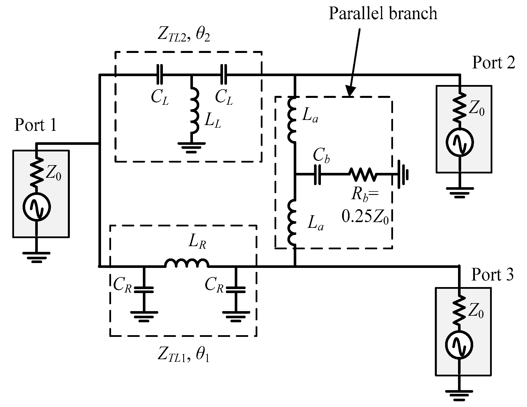
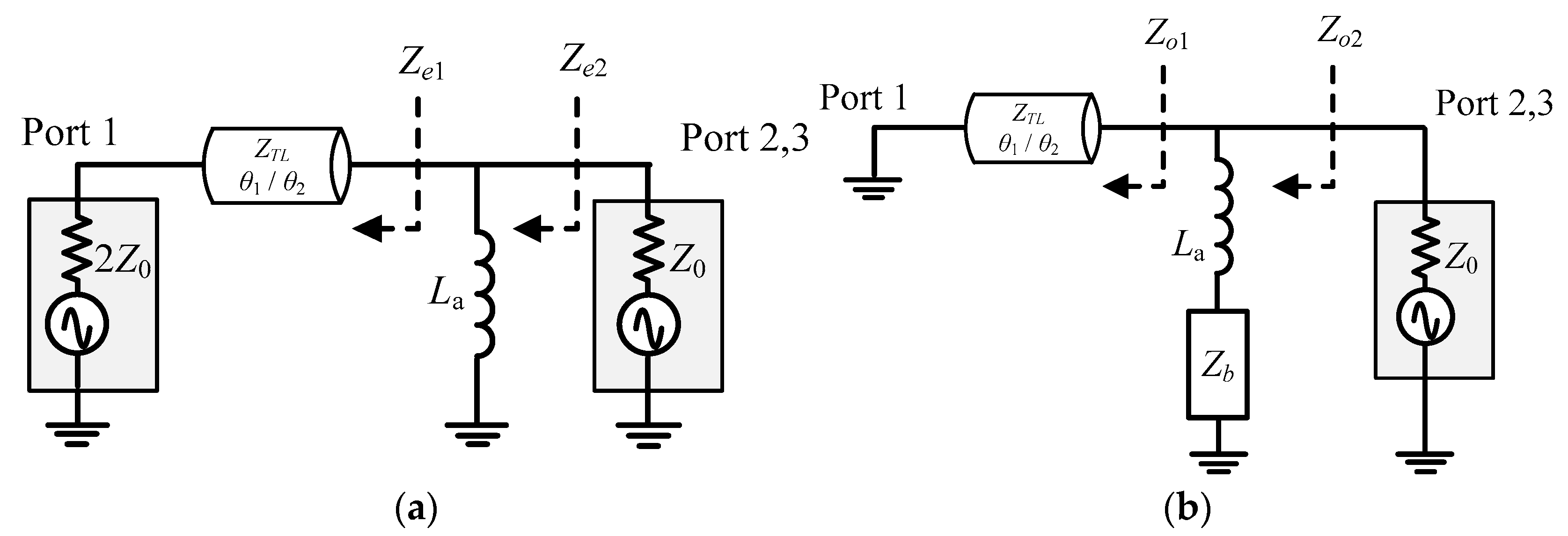
2. Wilkinson-Type Balun with Shorter Length Transmission Lines

Wilkinson-type baluns used 90°/−90° transmission lines in the serial branches and distributed lines with a resistor placed between the output ports (in parallel branch), as shown in Figure 1a. The lumped transmission lines are usually used when it is implemented on-chip, as shown in Figure 1b. The negative phase transmission line is implemented by a left-handed transmission line, while the positive one is replaced by a right-handed transmission line [5]. In the lumped transmission lines, the inductor occupies the largest area of the circuit.
To reduce the circuit size, two methods can be applied: (1) adjust the electrical length of the lumped-transmission line with a smaller inductor and/or (2) replace lumped transmission lines at the parallel branch with fewer components. In this paper, a new topology with these techniques was studied. The schematic is shown in Figure 2.
The phases of lumped transmission lines in Figure 2 are related by
θ 2 = θ 1 180
where θ 1 is the electrical length of the right-handed lumped-transmission line, while θ 2 is the electrical length of the left-handed one. The characteristic impedance of the lumped transmission lines and the lumped components can be found by even- and odd-mode analysis, shown in Figure 3.
The characteristic impedance of the transmission lines and the line electrical lengths, L a and Z b = R b + j X b , can be found from (2)–(5).
Z 0 = ω Z T L 2 L a tan ( θ ) 2 Z T L Z 0 2 ω L a Z 0 tan ( θ ) + 2 Z 0 Z T L ω L a Z T L 2 tan ( θ ) + ω L a Z T L 2 Z T L Z 0 2 ω L a Z 0 tan ( θ ) 2 + Z T L 2 tan ( θ ) + ω L a Z T L 2
Z T L 3 tan 2 ( θ ) 4 Z 0 2 + Z T L 2 ω L a tan ( θ ) 4 Z 0 2 + Z T L ω L a tan ( θ ) = 0
Z 0 R b 2 + Z T L tan ( θ ) + ω L a + X b 2 R b Z T L 2 t a n 2 ( θ ) = 0
ω L a + X b Z T L tan ( θ ) + ( ω L a + X b ) 2 + R b 2 = 0
All components in the circuit are related to each other. Variation in some components affects the performance of the circuit. In the manufacturing process, capacitor values are quite stable. On the other hand, the inductors have some variations in both their values and losses. The inductor losses have a major impact on the impedance matching and bandwidth of the overall circuit. Choosing different electrical length lines implies choosing different inductor values in the design. In the following, the impact of the inductors on the bandwidth and phase variation is studied numerically with four different designs.
The four different ideal lumped circuits operating at 6 GHz are shown in Table 1. The designs #1 with 60°/−120° and #2 with 75°/−105° are referred to in Figure 2. The design #3 with 90°/−90° using lumped transmission lines is referred to in Figure 1b, and the design #4 with 90°/−90° with a modified circuit is shown in Figure 4. Table 1 shows the design parameters with different Q values of the inductors. Their performances in terms of fractional bandwidth and maximum phase variation are summarized in Table 2. To identify the bandwidth, the −10 dB level for the reflection/isolation and 1.6 dB insertion loss were used.
In design #4, the two inductors, La, in Figure 2, were replaced with a common inductor. The ideal circuit with the 90°/−90° lines in Figure 2 cannot be realized with lumped components since the even and odd modes require open and short impedances in the parallel branch. With some losses, the structure in Figure 2 could be used. Nevertheless, the size of the inductors for the 90°/−90° design needed was larger than the others. To further reduce the size of the inductor La and improve the reflection losses, the circuit of design #4 was modified by replacing the inductors with a common inductor. The impedance matching in the even and odd modes can be easily controlled with the addition of the capacitor, Cb, and the resistor, Rb. A detailed analysis of the circuit can be found in [5].
It can be inferred from Table 2 that design #3 would have been one of the best performers among others if the inductors had been lossless. It had the smallest phase variation, but it had a major drawback of the smallest bandwidth with the Q value of 10. In addition, the exact parallel branch impedance was the key for the even and odd mode design methods. Design #3 needed the resonant effect in the even mode and impedance transformation of the lumped transmission lines in the parallel branch. Therefore, the component values needed to be precise to obtain the best performance. In practice, the implementation was difficult to accomplish because of many parasitic forms in the layout.
Generally, for the integrated passive device process, the quality factor of inductors was expected to be in the range of 15–20. Design #4 was chosen in implementing the arbitrary phase coupler so that the coupler would have a wider bandwidth with small phase variations. The matching impedance in the even- and odd-mode circuits with the layout parasitics and losses also makes the common inductor smaller. After the layout optimization, the design parameters at 6 GHz are CL1 = 0.394 pF, CL2 = 0.39 pF, LL = 1.876 nH, Cpl = 0.65 pF, CR1 = 0.246 pF, CR2 = 1 pF, LR = 1.876 nH, La = 1 nH, Lb = 0.385 nH, Cb = 1.23 pF, and Rb = 5.25 Ω. This balun was chosen as one of the building blocks for the differential phase coupler.

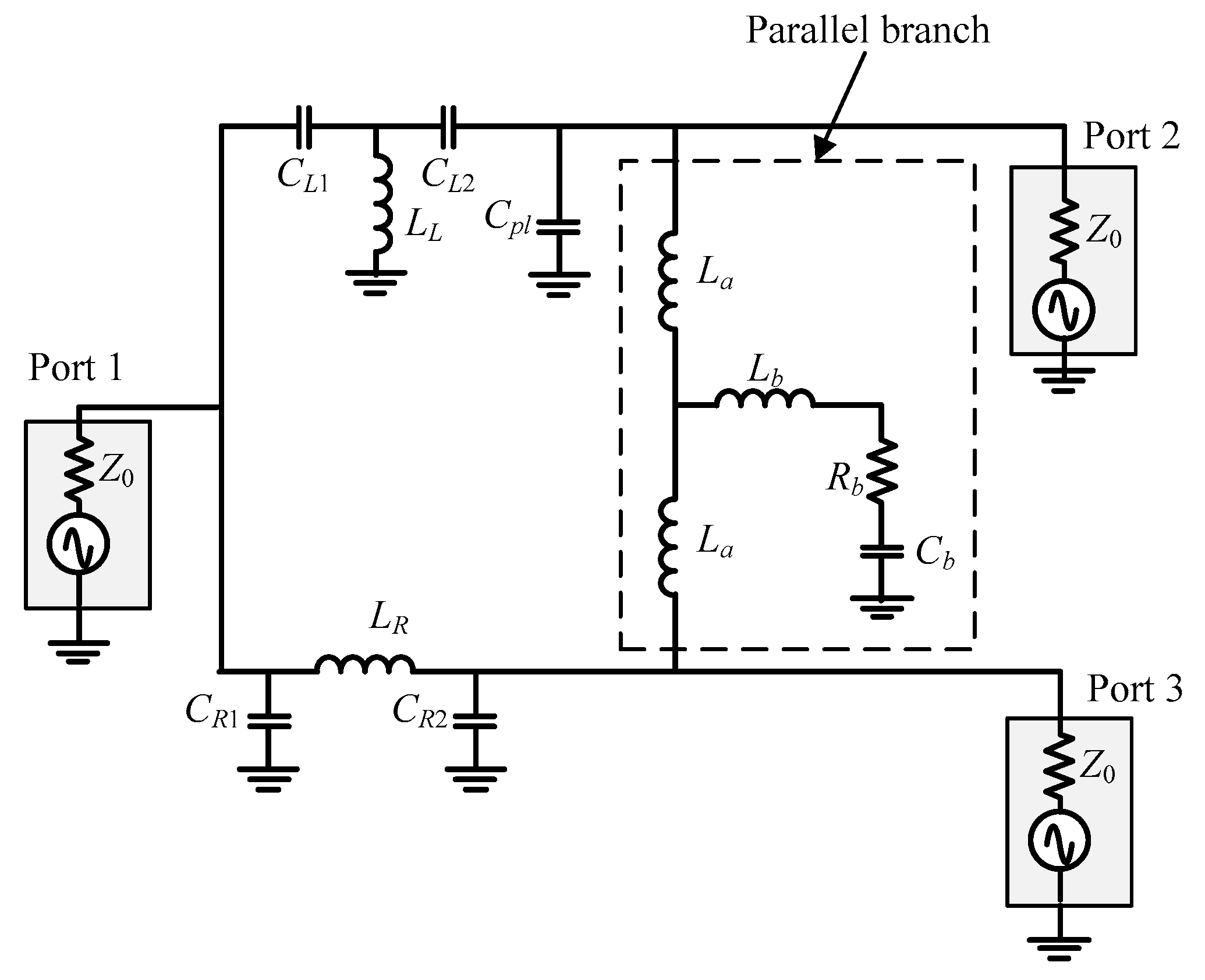
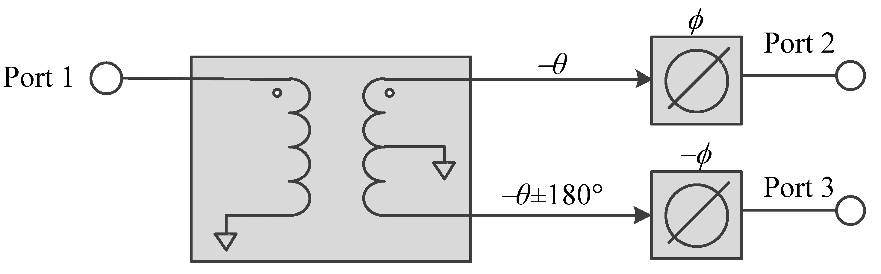
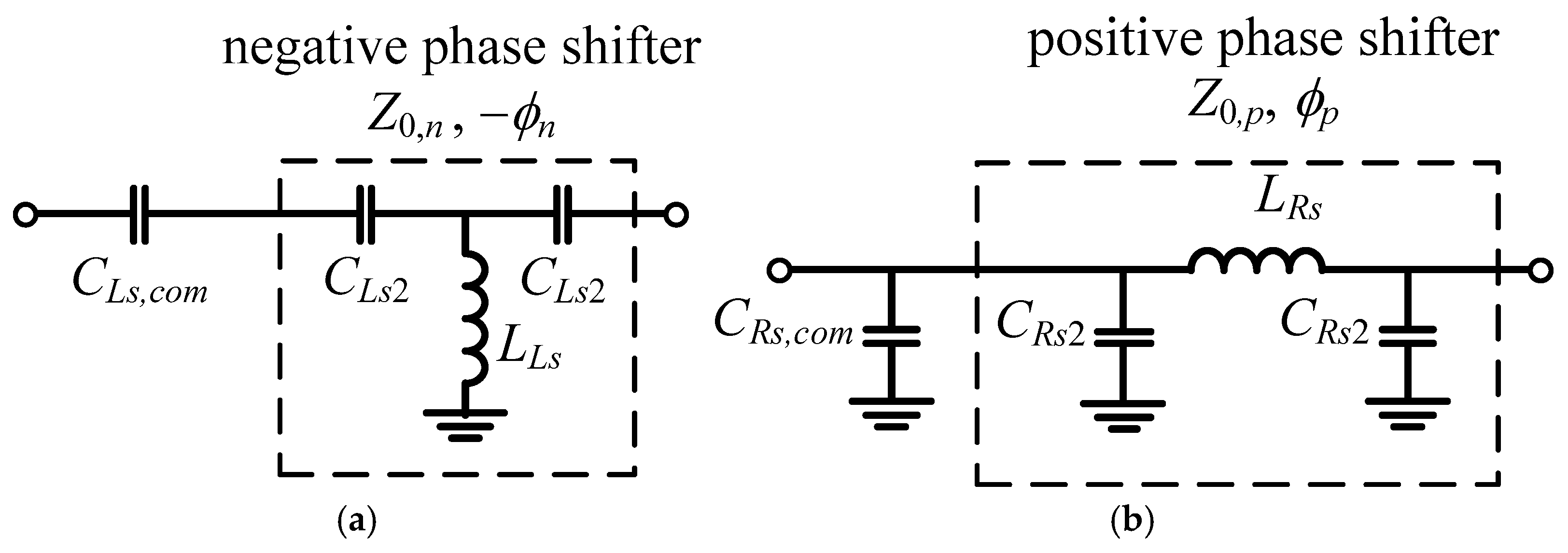
3. Differential Phase Coupler

The differential phase coupler consists of the balun and the phase shifters, as shown in Figure 5. Ideally, the phase shifters shown are lumped transmission lines with the same characteristic impedance as the port impedance and have the electrical length, ϕ. To achieve an output differential phase, ψ , the relationship between the output differential phase and the electrical length of the phase shifters, ϕ , is
ψ = 2 ϕ ± 180
Initially, the balun from design #4 in Table 2 with Q = 10 was used to cascade with phase shifters. The phase of the phase shifters was chosen to be opposite to those of the transmission lines of the balun so that the output phase difference between phase shifter #1 and phase shifter #2 was minimum ( 0 ° ψ 180 ° ).
In implementation, the output impedances of the balun were not perfectly equal to the port impedance due to the parasitic inductance from the connecting line in the layout. Compensation capacitors can be added before the phase shifter circuits, as shown in Figure 6. The phase shifter circuits are implemented by lumped transmission line circuits with Figure 6a for negative phase shift and Figure 6b for positive phase shift. The characteristic impedance of the line and the electrical length are shown in (7)–(10), where Z 0 , n and ϕ n are the characteristic impedance and negative phase of the phase shifter, while Z 0 , p and ϕ p are the characteristic impedance and positive phase of the phase shifters. In the design, the characteristic impedance of the lines is chosen to be the same as those of the port impedance.
C L S 2 = sin ϕ n ω Z 0 , n 1 cos ( ϕ n )
L L S = Z 0 , n ω sin ϕ n
C R s 2 = 1 ω Z 0 , p 1 cos ( ϕ p ) 1 + cos ( ϕ p )
L R s = Z 0 , p ω 1 cos 2 ( ϕ p )
In implementation, the compensation capacitors and the adjacent lumped transmission line capacitors are combined as shown in Figure 7. Their values are
C L s 1 = C L s , c o m C L s 2 C L s , c o m + C L s 2
C R s 1 = C R s , c o m + C R s 2
Therefore, the phase shifters also function as an impedance transformer. The negative phase shifter in Figure 7a was used as the phase shifter #2, while the positive phase in Figure 7b was used as the phase shifter #1 in Figure 5.
The block circuits in Figure 5 were implemented as the circuit shown in Figure 8. To test the design method, a quadrature coupler operating at 6 GHz was designed, fabricated, and measured.
The lumped components were adjusted to account for the layout parasitics. The design parameters at 6 GHz became CL1 = 1.53 pF, CL2 = 0.385 pF, LL = 1.635 nH, CR1 = 0.178 pF, CR2 = 0.98 pF, LR = 1.54 nH, La = 0.81 nH, Lb = 0.29 nH, Cb = 1.7 pF, and Rb = 7.2 Ω. The inductors were estimated to have Q ≈ 20. The resulting simulation and measurement are shown in Figure 9. In the figure, the measured data were added with ‘_mea’ in the legend, while the simulated data were added with ‘_sim’.
In Figure 9, the results from the measurement showed better matching at the input port than the simulated ones, while the measured reflection at the output ports was close to the simulated ones at the designed frequency. The transmission, the isolation, and the output phase difference were also in agreement. At the operating frequency, the measured results yielded reflection and isolation better than −19 dB, transmission better than −4.76 dB, and an output phase difference of 94.5°. Figure 10 shows the chip photo. The core size area was 989 μm × 893 μm. Table 3 shows the comparison between this work and others in the literature.
From the table, the designed hybrid coupler circuit of this work and [18] were implemented on-chip, while others were implemented on printed-circuit boards. The on-chip performance was expected to be inferior to those on PCB due to higher substrate loss. The reflection and isolation coefficients of this work were comparable with others, while the transmission coefficients were about 1 dB lower. The target phase difference was deviated by 4.5°. The chip size was only 0.02λ0 × 0.018λ0.

4. Conclusions

The three-port arbitrary phase coupler circuit on-chip was proposed in this paper. The circuit consists of a combination of balun and phase shifter circuits. Lumped-component Wilkinson-type baluns with lossy/lossless inductors were studied in this work. Three different transmission paths of the balun were also investigated. The ideal component simulations showed that the conventional transmission path length of 90°/−90° yielded the best performance. For layout implementation, a common inductor was used in the modified 90°/−90° circuit to reduce the size of the circuit. The phase shifter circuits were implemented by the modified right- and left-handed transmission lines. By choosing the line phase using the opposite signs to those of the transmission paths, the overall output phase difference could be kept minimal. With the proposed circuit, arbitrary phase outputs can be easily designed by adjusting the phase of the phase shifters.
An example circuit of a three-port 90° hybrid coupler was designed, fabricated, and measured. The measured chip showed a good performance compared with the others in the literature with a small size of 0.02 λ 0 × 0.018 λ 0 in the IPD process.

Author Contributions

Conceptualization, C.P. and S.W.; methodology, C.P.; validation, C.P. and C.-Y.C.; formal analysis, C.P.; investigation, C.P., C.-Y.C. and S.W.; resources, S.W.; writing—original draft preparation, C.P.; writing—review and editing, S.W.; visualization, C.P. and C.-Y.C.; supervision, S.W.; project administration, C.P. and S.W.; funding acquisition, C.P. and S.W. All authors have read and agreed to the published version of the manuscript.

Funding

This research is a result of the project entitled “Compact rat-race coupler circuit on lossy substrate (Year 1) Grant No. RE-KRIS/FF67/021” by King Mongkut’s Institute of Technology Ladkrabang (KMITL), which has been received funding support from the NSRF and in part by the National Taipei University of Technology-King Mongkut’s Institute of Technology Ladkrabang Joint Research Program (NTUT-KMITL) under Grant NTUT-KMITL-112-03, in part by the Research and Development Center for Smart Textile Technology of NTUT, and in part by the College of Advanced Manufacturing Innovation, King Mongkut’s Institute of Technology Ladkrabang.

Data Availability Statement

The original contributions presented in this study are included in the article. Further inquiries can be directed to the corresponding authors.

Acknowledgments

This work was supported in part by the College of Advanced Manufacturing Innovation, King Mongkut’s Institute of Technology Ladkrabang.

Conflicts of Interest

The authors declare no conflicts of interest.

References

  1. Chen, P.; Hong, W.; Zhang, H.; Chen, J.; Tang, H.; Chen, Z. Virtual phase shifter array and its application on Ku band mobile satellite reception. IEEE Trans. Antennas Propag. 2015, 63, 1408–1416. [Google Scholar] [CrossRef]
  2. Filippi, G.D.; Piotto, L.; Pirbazari, M.M.; Mazzanti, A. D-band RX front-end with a 0°–360° phase shifter based on programmable passive networks in SiGe-BiCMOS. IEEE Trans. Microw. Theory Tech. 2024, 72, 6205–6215. [Google Scholar] [CrossRef]
  3. Abbasi, M.; Lee, W. A low-loss passive D-band phase shifter for calibration-free, precise phase control. IEEE J. Solid-State Circuits 2024, 59, 1371–1380. [Google Scholar] [CrossRef]
  4. Lagana, F.; Bibbo, L.; Calcagno, S.; Carlo, D.D.; Pullano, S.A.; Prattico, D.; Angiulli, G. Smart electronic device-based monitoring of SAR and temperature variations in indoor human tissue interaction. Appl. Sci. 2025, 15, 2439. [Google Scholar] [CrossRef]
  5. Pakasiri, C.; Xu, J.-L.; Wang, S. A 10 GHz Compact Balun with Common Inductor on CMOS Process. Electronics 2023, 12, 468. [Google Scholar] [CrossRef]
  6. Gong, Y.; Cressler, J.D. A 60-GHz SiGe power amplifier with three-conductor transmission-line-based Wilkinson baluns and asymmetric directional couplers. IEEE Trans. Microw. Theory Tech. 2021, 69, 709–722. [Google Scholar] [CrossRef]
  7. Hsu, C.-Y.; Chen, C.-Y.; Chuang, H.-R. A 77-GHz CMOS on-chip bandpass filter with balanced and unbalanced outputs. IEEE Electron. Device Lett. 2010, 31, 1205–1207. [Google Scholar] [CrossRef]
  8. Xiong, W.; Dong, G.; Wang, Y.; Zhu, Z.; Yang, Y. 3-D compact marchand balun design based on through-silicon via technology for monolithic and 3-D integration. IEEE Trans. Very Large Scale Integr. (VLSI) Syst. 2022, 30, 1107–1118. [Google Scholar] [CrossRef]
  9. Hsu, H.-M.; Huang, J.-S.; Chen, S.-Y.; Lai, S.-H. Design of an on-chip balun with a minimum amplitude imbalance using a symmetric stack layout. IEEE Trans. Microw. Theory Tech. 2010, 58, 814–819. [Google Scholar]
  10. Cao, J.; Li, Z.; Li, Q.; Wang, Z. A wideband transformer balun with center open stub in CMOS process. IEEE Microw. Wirel. Compon. Lett. 2014, 24, 614–616. [Google Scholar] [CrossRef]
  11. Hossain, M.S.; Fujishima, M.; Yoshida, T.; Amakawa, S.; Rashid, M.M. Design of CMOS On-Chip Millimeter-Wave Transformer Coupled Balun and Power Divider-Combiner with Optimal Amplitude and Phase Imbalance. In Proceedings of the 2019 1st International Conference on Advances in Science, Engineering and Robotics Technology (ICASERT), Dhaka, Bangladesh, 3–5 May 2019. [Google Scholar]
  12. Li, S.; Xia, B.; Li, X.; Wang, Y.; Liu, X.; Chen, W. Analysis and design of broadband balance-compensated transformer baluns for silicon-based millimeter-wave circuits. IEEE Trans. Circuits Syst. I Reg. Pap. 2023, 70, 3103–3116. [Google Scholar] [CrossRef]
  13. Benaouf, T.M.; Hamdoun, A.; Himdi, M.; Lafond, O.; Ammor, H. Hybrid Coupler Used as Tunable Phase Shifter Based on Varactor Diodes. Micromachines 2024, 15, 838. [Google Scholar] [CrossRef] [PubMed]
  14. Jung, J.; Lee, G.; Song, J.-I. A lumped-element directional coupler with high isolation for mobile RFID reader. IEEE Microw. Wirel. Compon. Lett. 2014, 24, 382–384. [Google Scholar] [CrossRef]
  15. Sun, R.; Chen, Q.; Han, R.; Lu, Z. Analysis and design of wideband 90◦microstrip hybrid coupler. IEEE Access 2019, 7, 186409–186416. [Google Scholar] [CrossRef]
  16. Jafari, E.; Hodiatkashani, F.; Rezaiesarlak, R. A broadband quadrature hybrid using improved wideband Schiffman phase shifter. Prog. Electromagn. Res. C 2009, 11, 229–236. [Google Scholar] [CrossRef]
  17. Zhang, L.P.; Zhang, H.C.; Shao, C.; He, P.H.; Tang, M.; Mao, J.-F.; Cui, T.J. A broadband 90◦ balun with low-phase-imbalance performance based on periodic slow wave structure. IEEE Trans. Antennas Propag. 2021, 69, 4681–4687. [Google Scholar] [CrossRef]
  18. Xia, Z.; Wang, J.; Lu, Q.-Y.; Wu, W.; Hong, J. A wideband 90◦ phase shifting element applied in quadrature phase filtering power divider. IEEE Microw. Wirel. Compon. Lett. 2024, 34, 167–170. [Google Scholar] [CrossRef]
  19. Issakov, V.; Knapp, H.; Bakalski, W.; Wojnowski, M.; Thiede, A.; Simburger, W. Compact on-chip 90◦ and 180◦ splitters/combiners in silicon technology for 24 GHz applications. In Proceedings of the 40th European Microwave Conference, Paris, France, 28–30 September 2010. [Google Scholar]
  20. Qiu, L.-L.; Zhu, L.; Lyu, Y.-P. Differential phase shifters based on Schiffman type-C and type-F networks with wide phase shift range. Int. J. RF Microw. Comput. Aided Eng. 2020, 30, e22126. [Google Scholar] [CrossRef]
  21. Nebhen, J.; Ravelo, B. Innovative Microwave Design of Frequency-Independent Passive Phase Shifter with LCL-Network and Bandpass NGD Circuit. Prog. Electromagn. Res. C 2021, 109, 187–203. [Google Scholar] [CrossRef]
  22. Ravelo, B.; Guerin, M.; Frnda, J.; Sahao, F.E.; Fontgalland, G.; Silva, H.S.; Ngoho, S.; Haddad, F.; Rahajandraibe, W. Design method of constant phase-shifter microwave passive integrated circuit in 130-nm BiCMOS technology with bandpass-type negative group delay. IEEE Accesss 2022, 10, 93084–93103. [Google Scholar] [CrossRef]
  23. Guerin, M.; Rahajandraibe, W.; Fontgalland, G.; Silva, H.S.; Chan, G.; Wan, F.; Thakur, P.; Thakur, A.; Frnda, J.; Ravelo, B. Theory and original design of resistive-inductive network high-pass negative group delay integrated circuit in 130-nm CMOS technology. IEEE Access 2022, 10, 27147–27161. [Google Scholar] [CrossRef]
  24. Wan, F.; Gu, T.; Li, B.; Li, B.; Rahajandraibe, W.; Guerin, M.; Lallechere, S.; Ravelo, B. Design and experimentation of inductorless low-pass NGD integrated circuit in 180-nm CMOS technology. IEEE Trans. Comput.-Aided Design Integr. Circuits Syst. 2022, 41, 4965–4974. [Google Scholar] [CrossRef]
  25. Park, U. A Wilkinson-Type balun using a composite right/left-handed transmission line. J. Inf. Commun. Converg. Eng. 2013, 11, 147–152. [Google Scholar] [CrossRef]
  26. Caloz, C.; Itoh, T. Electromagnetic Metamaterials: Transmission Line Theory and Microwave Applications; Wiley-IEEE Press: Hoboken, NJ, USA, 2006. [Google Scholar]
Figure 1. Schematic of the Wilkinson-type balun with (a) distributed transmission lines form and (b) lumped transmission lines form.
Micromachines 16 00496 g001
Figure 2. Schematic of the reduced-phase lumped-transmission lines with lumped components at the parallel branch.
Micromachines 16 00496 g002
Figure 3. Schematics for the (a) even-mode and (b) odd-mode analysis.
Micromachines 16 00496 g003
Figure 4. Schematics for the modified balun circuit [5].
Micromachines 16 00496 g004
Figure 5. Diagram for the differential phase coupler.
Micromachines 16 00496 g005
Figure 6. Schematics for (a) negative phase shifter and (b) positive phase shifter with compensation capacitors.
Micromachines 16 00496 g006
Figure 7. Schematics for (a) negative phase shifter and (b) positive phase shifter with phase correction.
Micromachines 16 00496 g007
Figure 8. Schematics of the differential phase coupler.
Micromachines 16 00496 g008
Figure 9. Results from layout simulation and measurement. (a) |S11| (b) |S22| (c) |S33| (d) |S21|, |S31| (e) |S23| (f) output phase difference.
Micromachines 16 00496 g009aMicromachines 16 00496 g009b
Figure 10. Chip photo. The core chip area is 989 μm × 893 μm 0.02 λ 0 × 0.018 λ 0 .
Micromachines 16 00496 g010
Table 1. Various balun designs for different length transmission lines.
No.QTL1TL2Parallel Branch
LL
(nH)
(RL)
(Ω)
CL
(pF)
LR
(nH)
(RR)
(Ω)
CR
(pF)
La
(nH)
(Ra)
(Ω)
Cb
(pF)
Rb
(Ω)
#1
60°/−120°
ideal1.770.31.30.32.60.420
201.77
(3.33)
0.31.3
(2.5)
0.32.6
(5)
0.420
101.77
(6.66)
0.31.3
(5)
0.32.6
(10)
0.420
#2
75°/−105°
ideal1.90.31.70.36.70.224
201.9
(3.5)
0.31.7
(3.3)
0.36.7
(12.7)
0.224
101.9
(7)
0.31.7
(6.6)
0.36.7
(25.4)
0.224
#3
90°/−90°
ideal1.90.41.90.40.90.712.5
201.9
(3.5)
0.41.9
(3.5)
0.40.9
(1.8)
0.712.5
101.9
(7)
0.41.9
(7)
0.40.9
(3.5)
0.712.5
#4
90°/−90°
201.9
(3.5)
0.381.9
(3.5)
0.3814
(26.4)
0.111.7
101.9
(7)
0.381.8
(7)
0.3815.7
(59)
0.133.4
Table 2. Simulation results of the balun designs.
No.QFractional Bandwidth (%)Maximum Phase Deviation (°)
#1
60°/−120°
ideal32.845.31
2033.586.35
1034.7835.6
#2
75°/−105°
ideal21.141.99
2024.398.12
1025.8110.91
#3
90°/−90°
ideal401.83
2033.94.07
101.81.48
#4
90°/−90°
2033.041.281
1021.851.516
Table 3. Various 90° hybrid coupler designs.
References[15] *[16] **[17][18][19]This Work
ProcessPCBPCBPCBPCBCMOSIPD
TypePower divider and phase shifterPower divider and phase shifterPower divider and phase shifterCombined power divider and phase shifterTransformerBalun and phase shifter
f0
(GHz)
30.651.752.526.56
S21, S31
(dB)
>−3.5−3.2>−5>−4.68−3.5>−4.76
|S11|, |S22|, |S33| (dB)<−16−20<−15<−15−19<−18
|S23|
(dB)
<−20−25<−55<−20N/A<−20
Phase difference deviation
(degrees)
<52<3<50.64.5
Size
λ 0 2
0.2390.047N/A ***0.351.4 × 10−43.6 × 10⁻⁴
* Estimated values from Figures 12–14 [15]. ** Estimated values from Figures 4 and 6 [16]. *** No data available [17].
Disclaimer/Publisher’s Note: The statements, opinions and data contained in all publications are solely those of the individual author(s) and contributor(s) and not of MDPI and/or the editor(s). MDPI and/or the editor(s) disclaim responsibility for any injury to people or property resulting from any ideas, methods, instructions or products referred to in the content.

