
Metal/Perovskite Plasmonic–Photonic Heterostructures for Active and Passive Detection Devices


Abstract
1. Introduction
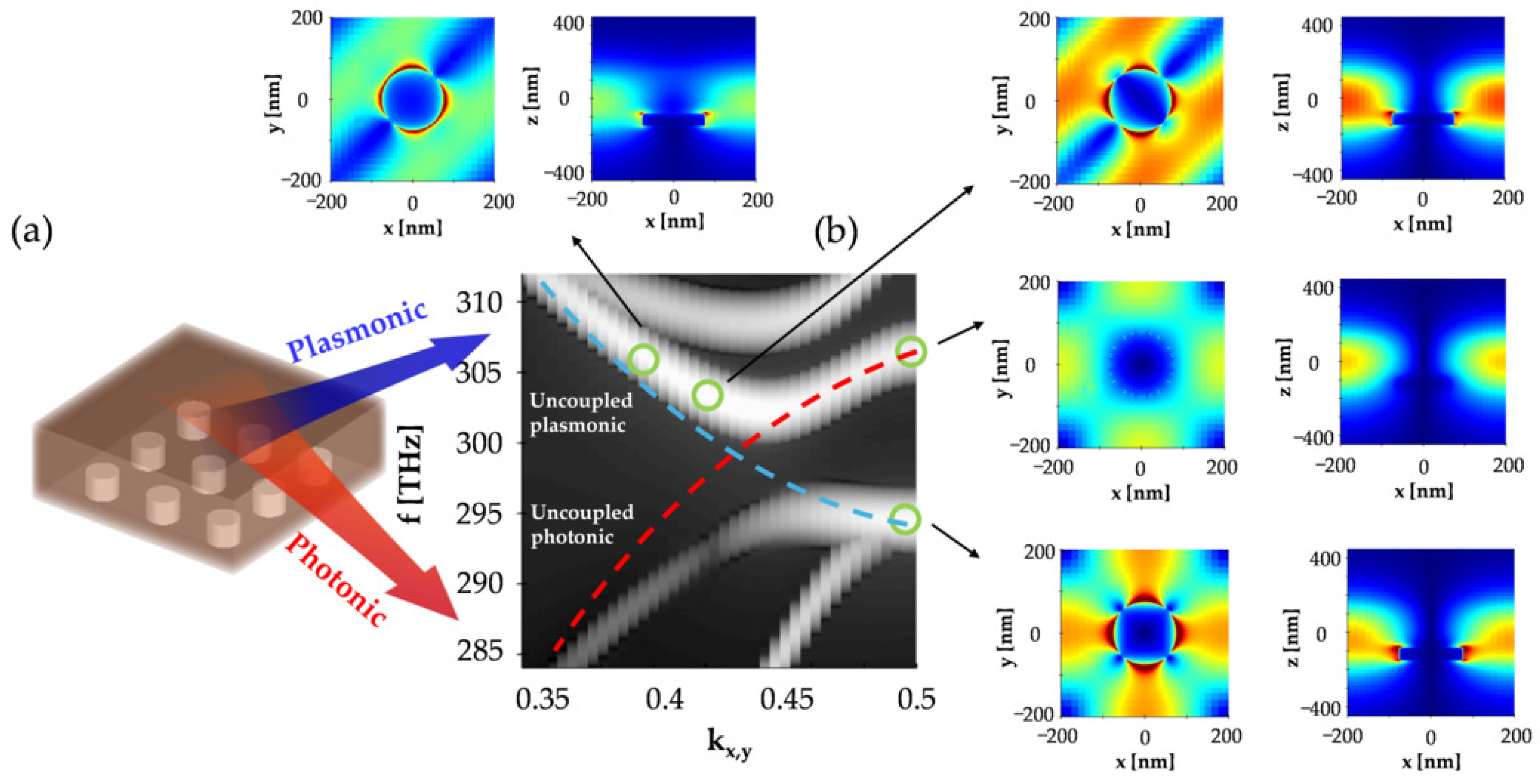
2. Design of the Hybrid Metasurface
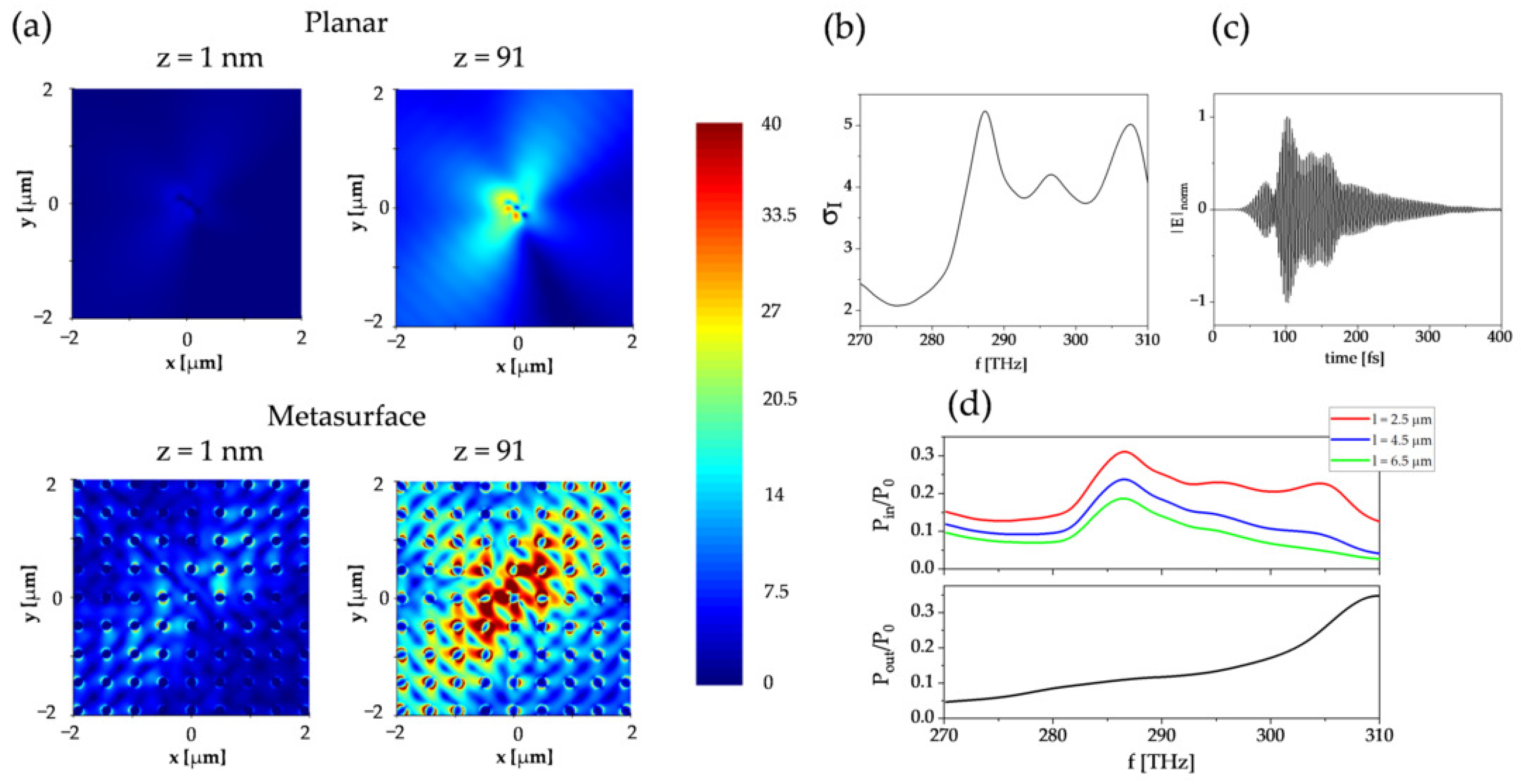
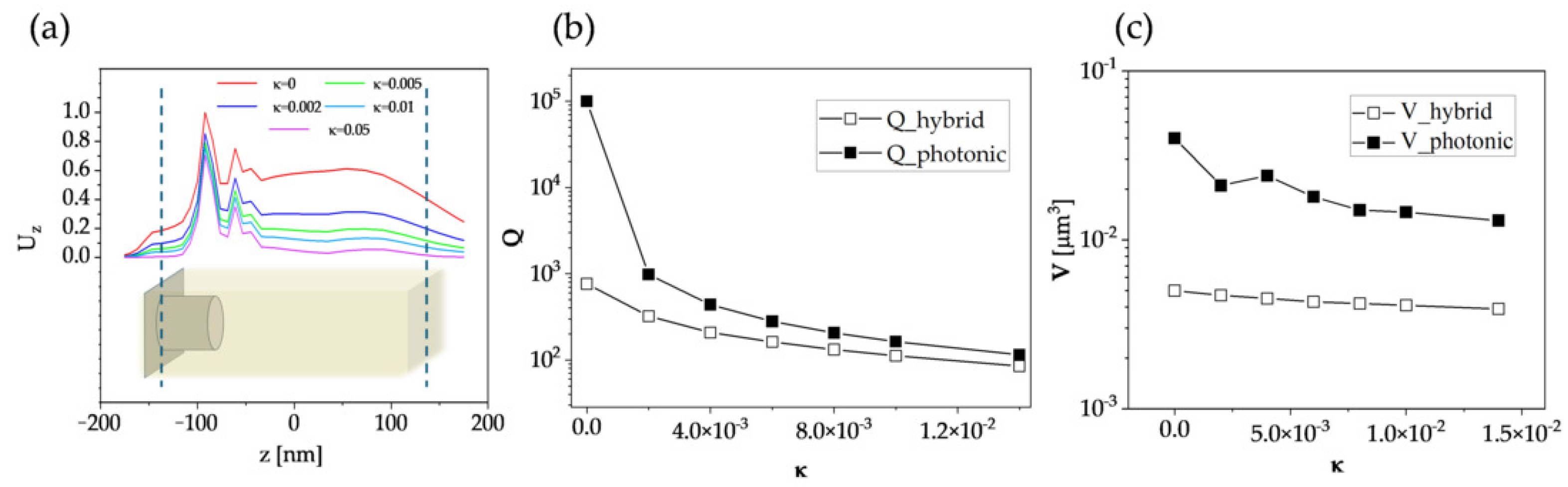
3. Field Confinement and Influence of Loss
4. Discussion
5. Methods
6. Conclusions
Author Contributions
Funding
Data Availability Statement
Conflicts of Interest
References
- Huang, Z.; Mao, Y.; Lin, G.; Yi, X.; Chang, A.; Li, C.; Chen, S.; Huang, W.; Wang, J. Low dark current broadband 360–1650 nm ITO/Ag/n-Si Schottky photodetectors. Opt. Express 2018, 26, 5827–5834. [Google Scholar] [CrossRef]
- Periyanagounder, D.; Gnanasekar, P.; Varadhan, P.; He, J.H.; Kulandaivel, J. High performance, self-powered photodetectors based on a graphene/silicon Schottky junction diode. J. Mater. Chem. C 2018, 6, 9545–9551. [Google Scholar] [CrossRef]
- Gao, W.; Zhang, S.; Zhang, F.; Wen, P.; Zhang, L.; Sun, Y.; Chen, H.; Zheng, Z.; Yang, M.; Luo, D.; et al. 2D WS2 Based Asymmetric Schottky Photodetector with High Performance. Adv. Electron. Mater. 2021, 7, 2000964. [Google Scholar] [CrossRef]
- Goykhman, I.; Desiatov, B.; Khurgin, J.; Shappir, J.; Levy, U. Waveguide based compact silicon Schottky photodetector with enhanced responsivity in the telecom spectral band. Opt. Express 2012, 20, 28594–28602. [Google Scholar] [CrossRef] [PubMed]
- Alavirad, M.; Olivieri, A.; Roy, L.; Berini, P. High-responsivity sub-bandgap hot-hole plasmonic Schottky detectors. Opt. Express 2016, 24, 22544–22554. [Google Scholar] [CrossRef] [PubMed]
- Frydendahl, C.; Grajower, M.; Bar-David, J.; Zektzer, R.; Mazurski, N.; Shappir, J.; Levy, U. Giant enhancement of silicon plasmonic shortwave infrared photodetection using nanoscale self-organized metallic films. Optica 2020, 7, 371–379. [Google Scholar] [CrossRef]
- Abubakr, E.; Abadi, A.; Oshita, M.; Saito, S.; Kan, T. Optimizing geometry and metal-dependent performance of Si-based Schottky plasmonic photodetectors. Opt. Mater. 2024, 150, 115175. [Google Scholar] [CrossRef]
- Wang, L.; Zhang, Y.; Wang, B.; Wei, Y.; Zhang, B.; Meng, L.; Liu, T.; Wang, B.; Han, B.; Jiang, Z.; et al. High-performance infrared Ge-based plasmonic photodetector enhanced by dual absorption mechanism. APL Photonics 2020, 5, 096104. [Google Scholar] [CrossRef]
- Levy, U.; Grajower, M.; Gonçalves, P.A.D.; Mortensen, N.A.; Khurgin, J.B. Plasmonic silicon Schottky photodetectors: The physics behind graphene enhanced internal photoemission. APL Photonics 2017, 2, 026103. [Google Scholar] [CrossRef]
- Ye, W.; Yong, Z.; Go, M.; Kowal, D.; Maddalena, F.; Tjahjana, L.; Wang, H.; Arramel, A.; Dujardin, C.; Birowosuto, M.D.; et al. The Nanoplasmonic Purcell Effect in Ultrafast and High-Light-Yield Perovskite Scintillators. Adv. Mater. 2024, 36, 2309410. [Google Scholar] [CrossRef]
- Makowski, M.; Ye, W.; Kowal, D.; Maddalena, F.; Mahato, S.; Amrillah, Y.T.; Zajac, W.; Witkowski, M.E.; Drozdowski, K.J.; Nathaniel; et al. Scaling Up Purcell-Enhanced Self-Assembled Nanoplasmonic Perovskite Scintillators into the Bulk Regime. arXiv 2024, arXiv:2411.18477. [Google Scholar]
- Hardhienata, H.; Ramdhani, I.; Alatas, H.; Faci, S.; Birowosuto, M.D. Investigating the Photovoltaic Performance in ABO3 Structures via the Nonlinear Bond Model for an Arbitrary Incoming Light Polarization. Micromachines 2023, 14, 2063. [Google Scholar] [CrossRef] [PubMed]
- Ai, B.; Fan, Z.; Wong, Z.J. Plasmonic–perovskite solar cells, light emitters, and sensors. Microsyst. Nanoeng. 2022, 8, 5. [Google Scholar] [CrossRef] [PubMed]
- Shahriyari, H.; Hatefi-Kargan, N.; Daraei, A. Plasmonic graphene/perovskite Schottky barrier photodetector. Z. Naturforsch. A 2024, 79, 815–821. [Google Scholar] [CrossRef]
- Gu, Q.; Hu, C.; Yang, J.; Lv, J.; Ying, Y.; Jiang, X.; Si, G. Plasmon enhanced perovskite-metallic photodetectors. Mater. Des. 2021, 198, 109374. [Google Scholar] [CrossRef]
- Park, Y.; Choi, J.; Kang, M.; Lee, H.; Ihee, H.; Park, J.Y. Relaxation Dynamics of Enhanced Hot-Electron Flow on Perovskite-Coupled Plasmonic Silver Schottky Nanodiodes. J. Phys. Chem. C 2021, 125, 2575–2582. [Google Scholar] [CrossRef]
- Zeng, L.H.; Chen, Q.M.; Zhang, Z.X.; Wu, D.; Yuan, H.; Li, Y.Y.; Qarony, W.; Lau, S.P.; Luo, L.B.; Tsang, Y.H. Multilayered PdSe2/Perovskite Schottky Junction for Fast, Self-Powered, Polarization-Sensitive, Broadband Photodetectors, and Image Sensor Application. Adv. Sci. 2019, 6, 1901134. [Google Scholar] [CrossRef]
- Wu, S.; Chen, C.; Dai, Y.; Ye, J.; Xu, X.; Liu, X.; Tian, F.; Xu, Y.; Hu, H. Direct-detected spectroscopy based on a plasmonic Schottky photodetector and a deep neural network. Opt. Lett. 2023, 48, 4965–4968. [Google Scholar] [CrossRef]
- Gosciniak, J.; Atar, F.B.; Corbett, B.; Rasras, M. Plasmonic Schottky photodetector with metal stripe embedded into semiconductor and with a CMOS-compatible titanium nitride. Sci. Rep. 2019, 9, 6048. [Google Scholar] [CrossRef]
- Goykhman, I.; Sassi, U.; Desiatov, B.; Mazurski, N.; Milana, S.; De Fazio, D.; Eiden, A.; Khurgin, J.; Shappir, J.; Levy, U.; et al. On-Chip Integrated, Silicon-Graphene Plasmonic Schottky Photodetector with High Responsivity and Avalanche Photogain. Nano Lett. 2016, 16, 3005–3013. [Google Scholar] [CrossRef]
- Lan, Z.; Lei, Y.; Chan, W.K.E.; Chen, S.; Luo, D.; Zhu, F. Near-infrared and visible light dual-mode organic photodetectors. Sci. Adv. 2020, 6, eaaw8065. [Google Scholar] [CrossRef]
- Cherqui, C.; Bourgeois, M.R.; Wang, D.; Schatz, G.C. Plasmonic Surface Lattice Resonances: Theory and Computation. Acc. Chem. Res. 2019, 52, 2548–2558. [Google Scholar] [CrossRef] [PubMed]
- Kravets, V.; Kabashin, A.; Barnes, W.; Grigorenko, A. Plasmonic Surface Lattice Resonances: A Review of Properties and Applications. Chem. Rev. 2018, 118, 5912–5951. [Google Scholar] [CrossRef] [PubMed]
- Le-Van, Q.; Zoethout, E.; Geluk, E.J.; Ramezani, M.; Berghuis, M.; Gómez Rivas, J. Enhanced Quality Factors of Surface Lattice Resonances in Plasmonic Arrays of Nanoparticles. Adv. Opt. Mater. 2019, 7, 1801451. [Google Scholar] [CrossRef]
- Yanagawa, H.; Hinamoto, T.; Kanno, T.; Sugimoto, H.; Shioi, M.; Fujii, M. Gold nanopillar array with sharp surface plasmon resonances and the application in immunoassay. J. Appl. Phys. 2019, 126, 223104. [Google Scholar] [CrossRef]
- Azzam, S.I.; Shalaev, V.M.; Boltasseva, A.; Kildishev, A.V. Formation of Bound States in the Continuum in Hybrid Plasmonic-Photonic Systems. Phys. Rev. Lett. 2018, 121, 253901. [Google Scholar] [CrossRef] [PubMed]
- Tuniz, A.; Song, A.Y.; Della Valle, G.; de Sterke, C.M. Coupled mode theory for plasmonic couplers. Appl. Phys. Rev. 2024, 11, 021309. [Google Scholar] [CrossRef]
- Chen, C.; Oh, S.H.; Li, M. Coupled-mode theory for plasmonic resonators integrated with silicon waveguides towards mid-infrared spectroscopic sensing. Opt. Express 2020, 28, 2020–2036. [Google Scholar] [CrossRef]
- Wu, Y.; Yan, X.; Zhang, X.; Ren, X. A monolayer graphene/GaAs nanowire array Schottky junction self-powered photodetector. Appl. Phys. Lett. 2016, 109, 183101. [Google Scholar] [CrossRef]
- Wang, B.; Zhang, J.; Lian, S.; Wu, H.; Liu, Z.; Wang, G. Patterned 3D-graphene for self-powered broadband photodetector. Appl. Phys. Lett. 2024, 125, 142103. [Google Scholar] [CrossRef]
- Frolova, L.A.; Davlethanov, A.I.; Dremova, N.N.; Zhidkov, I.; Akbulatov, A.F.; Kurmaev, E.Z.; Aldoshin, S.M.; Stevenson, K.J.; Troshin, P.A. Efficient and Stable MAPbI3-Based Perovskite Solar Cells Using Polyvinylcarbazole Passivation. J. Phys. Chem. Lett. 2020, 11, 6772–6778. [Google Scholar] [CrossRef]
- Morteza Najarian, A.; Dinic, F.; Chen, H.; Sabatini, R.; Zheng, C.; Lough, A.; Maris, T.; Saidaminov, M.I.; García de Arquer, F.P.; Voznyy, O.; et al. Homomeric chains of intermolecular bonds scaffold octahedral germanium perovskites. Nature 2023, 620, 328–335. [Google Scholar] [CrossRef]
- Singh, J.K.; Mandal, S.K.; Banerjee, G. Refractive index of different perovskite materials. J. Mater. Res. 2021, 36, 1773–1793. [Google Scholar] [CrossRef]
- Dagnall, K.A.; Conley, A.M.; Yoon, L.U.; Rajeev, H.S.; Lee, S.H.; Choi, J.J. Ytterbium-Doped Cesium Lead Chloride Perovskite as an X-ray Scintillator with High Light Yield. ACS Omega 2022, 7, 20968–20974. [Google Scholar] [CrossRef] [PubMed]
- Haposan, T.; Arramel, A.; Maulida, P.Y.D.; Hartati, S.; Afkauni, A.A.; Mahyuddin, M.H.; Zhang, L.; Kowal, D.; Witkowski, M.E.; Drozdowski, K.J.; et al. All-inorganic copper-halide perovskites for large-Stokes shift and ten-nanosecond-emission scintillators. J. Mater. Chem. C 2024, 12, 2398–2409. [Google Scholar] [CrossRef]
- Zhao, F.; Luo, X.; Gu, C.; Chen, J.; Hu, Z.; Peng, Y. Novel 3D Printing Encapsulation Strategies for Perovskite Photodetectors. Adv. Mater. Technol. 2022, 7, 2200521. [Google Scholar] [CrossRef]
- Khan, A.A.; Kumar, N.; Jung, U.; Heo, W.; Tan, Z.; Park, J. Performance and stability enhancement of perovskite photodetectors by additive and interface engineering using a dual-functional PPS zwitterion. Nanoscale Horiz. 2023, 8, 1577–1587. [Google Scholar] [CrossRef]
- Li, X.; Liu, C.; Ding, F.; Lu, Z.; Gao, P.; Huang, Z.; Dang, W.; Zhang, L.; Lin, X.; Ding, S.; et al. Ultra-Stable and Sensitive Ultraviolet Photodetectors Based on Monocrystalline Perovskite Thin Films. Adv. Funct. Mater. 2023, 33, 2213360. [Google Scholar] [CrossRef]
- Al Amin, N.R.; Lee, C.C.; Huang, Y.C.; Shih, C.J.; Estrada, R.; Biring, S.; Kuo, M.H.; Li, C.F.; Huang, Y.C.; Liu, S.W. Achieving a Highly Stable Perovskite Photodetector with a Long Lifetime Fabricated via an All-Vacuum Deposition Process. ACS Appl. Mater. Interfaces 2023, 15, 21284–21295. [Google Scholar] [CrossRef]
- Kowal, D.; Mahato, S.; Makowski, M.; Hartati, S.; Sheikh, M.A.K.; Ye, W.; Schaart, D.R.; Cybinska, J.; Wong, L.J.; Arramel, A.; et al. Current trends in material research for nuclear batteries: Harnessing metal perovskite halides and other chalcogenides for greater compactness and efficiency. Appl. Phys. Rev. 2025, 12, 011328. [Google Scholar] [CrossRef]

Disclaimer/Publisher’s Note: The statements, opinions and data contained in all publications are solely those of the individual author(s) and contributor(s) and not of MDPI and/or the editor(s). MDPI and/or the editor(s) disclaim responsibility for any injury to people or property resulting from any ideas, methods, instructions or products referred to in the content. |
© 2025 by the authors. Licensee MDPI, Basel, Switzerland. This article is an open access article distributed under the terms and conditions of the Creative Commons Attribution (CC BY) license (https://creativecommons.org/licenses/by/4.0/).
Share and Cite
Kowal, D.; Chen, Y.; Birowosuto, M.D. Metal/Perovskite Plasmonic–Photonic Heterostructures for Active and Passive Detection Devices. Micromachines 2025, 16, 424. https://doi.org/10.3390/mi16040424
Kowal D, Chen Y, Birowosuto MD. Metal/Perovskite Plasmonic–Photonic Heterostructures for Active and Passive Detection Devices. Micromachines. 2025; 16(4):424. https://doi.org/10.3390/mi16040424
Chicago/Turabian StyleKowal, Dominik, Yuntian Chen, and Muhammad Danang Birowosuto. 2025. "Metal/Perovskite Plasmonic–Photonic Heterostructures for Active and Passive Detection Devices" Micromachines 16, no. 4: 424. https://doi.org/10.3390/mi16040424
APA StyleKowal, D., Chen, Y., & Birowosuto, M. D. (2025). Metal/Perovskite Plasmonic–Photonic Heterostructures for Active and Passive Detection Devices. Micromachines, 16(4), 424. https://doi.org/10.3390/mi16040424