
Status of Extended Threshold Wavelength Split-Off Band IR Detectors and Quantum Material-Based Extension for Room-Temperature Operation

Abstract
1. Introduction
2. Benchmarks of Split-Off Band IR Detection
 ), SP1 (
 ), and SP2 (
 )) and the fitting results (solid red lines) by using Equation (1). With the experimental data of λt, λeff, and Δ for HE0204, SP1, and SP2, (16.1 µm, 8.2 µm, and 6.0 µm, respectively) substituted, the fitting curves shows excellent agreement with the experimental observations. A simulated dark current for a modeled symmetric detector (labeled as M) of Δ = 0.091 eV (13.7 µm) is also shown by the dotted green (•••) line in Figure 2. The dark current data for the sample LH1002 and the photoresponse spectra for listed samples (Table 1) are available in earlier reports [1,2,3,38]. This analysis indicates that the 3D carrier drift model can successfully explain the dark current behavior of the symmetric AlGaAs heterostructures.
2.1. Effect of the Barrier Energy Offset (with Flat Injector Barrier)
2.2. Advantages in Dark Current and D* with Increased Barrier Energy Offset
2.3. Effect of the Gradient of the Injector Barrier (with the Same Barrier Energy Offset)
3. An Empirical Model for Hot-Hole Effects in the IR Sensor
4. Challenges of Visions
- In the AlxGa1-xAs IR detectors, the spectral extension and dark current level can be controlled independently through the parameters of Δ and δEV, as labeled in Figure 1d. Although the dark current level can be decreased without changing the threshold wavelength by increasing Δ while maintaining the same δEV (and thus, Δ′), the attainable Δ in the original AlxGa1-xAs is limited to 0.4 eV, beyond which a direct-to-indirect band transition occurs. Consequently, the AlGaAs sensors showed a detectivity of only ~105 Jones in the 3–5 µm range at room temperature [44].
- The extension of spectral response requires the hot-hole mean-free path to be longer than their traveling length in the absorber layer (x2–x3 region in Figure 1c,d) to prevent relaxation and effectively create the quasi-Fermi level. A narrower AlGaAs absorber design can easily fulfill this request, but the scattering on the heterojunction interfaces will introduce another bottleneck. The island growth during the GaAs/AlGaAs MBE process could also create interfacial roughness that acts as a defect scattering the hot holes [45,46], either dissipating their energy or elongating their trajectory inside the absorber, hindering the device performance.
- The IR detectors with all the above-mentioned advantages fundamentally rely on the intra-band transition, which is enabled by the spin–orbit interaction-induced split-off band. All theoretical analysis about the quasi-Fermi level formation and dark current benefits is also based on this assumption. On the other hand, the system still lacks sufficient tunability on the split-off band in AlGaAs materials. Consequently, uncertainties about feasibility and versatility still exist in the above-introduced theoretical model.
4.1. The Emergence of van der Waals Quantum Materials (vdW-QMs)
4.2. The Design of vdW-QMs Based Heterostructures
4.3. Dark Current Suppression
4.4. Formation of Quasi-Fermi Level and IR Extension at Room Temperature via Structural Optimization
5. Conclusions
Author Contributions
Funding
Conflicts of Interest
References
- Rogalski, A. HgCdTe infrared detector material: History, status and outlook. Rep. Prog. Phys. 2005, 68, 2267. [Google Scholar] [CrossRef]
- Kinch, M.A. The Future of Infrared; III–Vs or HgCdTe? J. Electron. Mater. 2015, 44, 2969–2976. [Google Scholar] [CrossRef]
- Zhang, J.; Itzler, M.A.; Zbinden, H.; Pan, J.-W. Advances in InGaAs/InP single-photon detector systems for quantum communication. Light Sci. Appl. 2015, 4, e286. [Google Scholar] [CrossRef]
- Evirgen, A.; Abautret, J.; Perez, J.P.; Cordat, A.; Nedelcu, A.; Christol, P. Midwave infrared InSb nBn photodetector. Electron. Lett. 2014, 50, 1472–1473. [Google Scholar] [CrossRef]
- Schneider, H.; Liu, H.C. Quantum Well Infrared Photodetectors; Springer: Berlin/Heidelberg, Germany, 2007. [Google Scholar]
- Gunapala, S.; Bandara, S.; Rafol, S.; Ting, D. Quantum well infrared photodetectors. In Semiconductors and Semimetals; Elsevier: Amsterdam, The Netherlands, 2011; Volume 84, pp. 59–151. [Google Scholar]
- Francombe, M.H. Handbook of Thin Film Devices; Academic Press: Cambridge, MA, USA, 2000. [Google Scholar]
- Perera, A.U.; Liu, H. Semiconductor Optical and Electro-Optical Devices; Academic Press: Cambridge, MA, USA, 2000; Volume 2. [Google Scholar]
- Choi, K.-K. The Physics of Quantum Well Infrared Photodetectors; World Scientific: Singapore, 1997; Volume 7. [Google Scholar]
- Levine, B.F. Quantum-well infrared photodetectors. J. Appl. Phys. 1993, 74, R1–R81. [Google Scholar] [CrossRef]
- Kwan, D.; Kesaria, M.; Anyebe, E.A.; Huffaker, D. Recent trends in 8–14 μm type-II superlattice infrared detectors. Infrared Phys. Technol. 2021, 116, 103756. [Google Scholar] [CrossRef]
- Smith, D.L.; Mailhiot, C. Proposal for strained type II superlattice infrared detectors. J. Appl. Phys. 1987, 62, 2545–2548. [Google Scholar] [CrossRef]
- Wei, Y.; Gin, A.; Razeghi, M.; Brown, G.J. Type II InAs/GaSb superlattice photovoltaic detectors with cutoff wavelength approaching 32 μm. Appl. Phys. Lett. 2002, 81, 3675–3677. [Google Scholar] [CrossRef]
- Rogalski, A.; Martyniuk, P.; Kopytko, M. InAs/GaSb type-II superlattice infrared detectors: Future prospect. Appl. Phys. Rev. 2017, 4, 031304. [Google Scholar] [CrossRef]
- Lao, Y.-F.; Perera, A.G.U.; Li, L.H.; Khanna, S.P.; Linfield, E.H.; Liu, H.C. Tunable hot-carrier photodetection beyond the bandgap spectral limit. Nat. Photonics 2014, 8, 412–418. [Google Scholar] [CrossRef]
- Lao, Y.F.; Pitigala, P.K.D.D.P.; Perera, A.G.U.; Liu, H.C.; Buchanan, M.; Wasilewski, Z.R.; Choi, K.K.; Wijewarnasuriya, P. Light-hole and heavy-hole transitions for high-temperature long-wavelength infrared detection. Appl. Phys. Lett. 2010, 97, 091104. [Google Scholar] [CrossRef]
- Perera, A.G.U.; Matsik, S.G.; Jayaweera, P.V.V.; Tennakone, K.; Liu, H.C.; Buchanan, M.; Von Winckel, G.; Stintz, A.; Krishna, S. High operating temperature split-off band infrared detectors. Appl. Phys. Lett. 2006, 89, 131118. [Google Scholar] [CrossRef]
- Matsik, S.; Jayaweera, P.; Perera, A.; Choi, K.; Wijewarnasuriya, P. Device modeling for split-off band detectors. J. Appl. Phys. 2009, 106, 064503. [Google Scholar] [CrossRef]
- Jayaweera, P.; Matsik, S.; Perera, A.; Liu, H.; Buchanan, M.; Wasilewski, Z. Uncooled infrared detectors for 3–5 μm and beyond. Appl. Phys. Lett. 2008, 93, 021105. [Google Scholar] [CrossRef]
- Liu, H.; Dupont, E.; Byloos, M.; Buchanan, M.; Song, C.-Y.; Wasilewski, Z. QWIP-LED pixelless thermal imaging device. Int. J. High Speed Electron. Syst. 2002, 12, 891–905. [Google Scholar] [CrossRef]
- Rao, T.; Chen, M.; Mu, G.; Tang, X. Infrared-to-visible upconversion devices. Coatings 2022, 12, 456. [Google Scholar] [CrossRef]
- Somvanshi, D.; Chauhan, D.; Lao, Y.-F.; Perera, A.G.U.; Li, L.; Khanna, S.P.; Linfield, E.H. Analysis of Extended Threshold Wavelength Photoresponse in Nonsymmetrical p-GaAs/AlGaAs Heterostructure Photodetectors. IEEE J. Sel. Top. Quantum Electron. 2018, 24, 1–7. [Google Scholar] [CrossRef]
- Chauhan, D.; Perera, A.G.U.; Li, L.; Chen, L.; Khanna, S.P.; Linfield, E.H. Extended wavelength infrared photodetectors. Opt. Eng. 2017, 56, 091605. [Google Scholar] [CrossRef]
- Rinzan, M.B.M.; Perera, A.G.U.; Matsik, S.G.; Liu, H.C.; Wasilewski, Z.R.; Buchanan, M. AlGaAs emitter∕GaAs barrier terahertz detector with a 2.3 THz threshold. Appl. Phys. Lett. 2005, 86, 071112. [Google Scholar] [CrossRef]
- Perera, A.G.U.; Yuan, H.X.; Gamage, S.K.; Shen, W.Z.; Francombe, M.H.; Liu, H.C.; Buchanan, M.; Schaff, W.J. GaAs multilayer p+-i homojunction far-infrared detectors. J. Appl. Phys. 1997, 81, 3316–3319. [Google Scholar] [CrossRef]
- Lao, Y.-F.; Perera, A.G.U. Temperature-dependent internal photoemission probe for band parameters. Phys. Rev. B 2012, 86, 195315. [Google Scholar] [CrossRef]
- Esaev, D.G.; Rinzan, M.B.M.; Matsik, S.G.; Perera, A.G.U. Design and optimization of GaAs∕AlGaAs heterojunction infrared detectors. J. Appl. Phys. 2004, 96, 4588–4597. [Google Scholar] [CrossRef]
- Lei, S.; Ge, L.; Najmaei, S.; George, A.; Kappera, R.; Lou, J.; Chhowalla, M.; Yamaguchi, H.; Gupta, G.; Vajtai, R. Evolution of the electronic band structure and efficient photo-detection in atomic layers of InSe. ACS Nano 2014, 8, 1263–1272. [Google Scholar] [CrossRef] [PubMed]
- Nair, R.R.; Blake, P.; Grigorenko, A.N.; Novoselov, K.S.; Booth, T.J.; Stauber, T.; Peres, N.M.; Geim, A.K. Fine structure constant defines visual transparency of graphene. Science 2008, 320, 1308. [Google Scholar] [CrossRef]
- Piper, J.R.; Fan, S. Broadband absorption enhancement in solar cells with an atomically thin active layer. Acs Photonics 2016, 3, 571–577. [Google Scholar] [CrossRef]
- Lei, S.; Wen, F.; Ge, L.; Najmaei, S.; George, A.; Gong, Y.; Gao, W.; Jin, Z.; Li, B.; Lou, J. An atomically layered InSe avalanche photodetector. Nano Lett. 2015, 15, 3048–3055. [Google Scholar] [CrossRef]
- Guo, Q.; Pospischil, A.; Bhuiyan, M.; Jiang, H.; Tian, H.; Farmer, D.; Deng, B.; Li, C.; Han, S.-J.; Wang, H.; et al. Black Phosphorus Mid-Infrared Photodetectors with High Gain. Nano Lett. 2016, 16, 4648–4655. [Google Scholar] [CrossRef]
- Ma, C.; Yuan, S.; Cheung, P.; Watanabe, K.; Taniguchi, T.; Zhang, F.; Xia, F. Intelligent infrared sensing enabled by tunable moiré quantum geometry. Nature 2022, 604, 266–272. [Google Scholar] [CrossRef]
- Yan, H.; Xia, F.; Zhu, W.; Freitag, M.; Dimitrakopoulos, C.; Bol, A.A.; Tulevski, G.; Avouris, P. Infrared spectroscopy of wafer-scale graphene. ACS Nano 2011, 5, 9854–9860. [Google Scholar] [CrossRef]
- Chauhan, D.; Perera, A.; Li, L.; Chen, L.; Linfield, E. Dark current and photoresponse characteristics of extended wavelength infrared photodetectors. J. Appl. Phys. 2017, 122, 024501. [Google Scholar] [CrossRef]
- Somvanshi, D.; Chauhan, D.; Perera, A.G.U.; Li, L.; Chen, L.; Linfield, E.H. Analysis of Barrier Parameters on the Extended Threshold Wavelength of Infrared Detectors. IEEE Photonics Technol. Lett. 2018, 30, 1617–1620. [Google Scholar] [CrossRef]
- Perera, A.G.U. Heterojunction and superlattice detectors for infrared to ultraviolet. Prog. Quantum Electron. 2016, 48, 1–56. [Google Scholar] [CrossRef]
- Chauhan, D.; Perera, A.G.U.; Li, L.H.; Chen, L.; Linfield, E.H. Study of infrared photodetectors with wavelength extension mechanism. Infrared Phys. Technol. 2018, 95, 148–151. [Google Scholar] [CrossRef]
- Somvanshi, D.; Chauhan, D.; Perera, A.G.U.; Li, L.; Chen, L.; Linfield, E.H. Reduced Dark Current With a Specific Detectivity Advantage in Extended Threshold Wavelength Infrared Detector. IEEE Sens. Lett. 2019, 3, 1–4. [Google Scholar] [CrossRef]
- Rinzan, M.B.; Matsik, S.; Perera, A.G.U. Quantum mechanical effects in internal photoemission THz detectors. Infrared Phys. Technol. 2007, 50, 199–205. [Google Scholar] [CrossRef]
- Apalkov, V.; Ariyawansa, G.; Perera, A.G.U.; Buchanan, M.; Wasilewski, Z.R.; Liu, H.C. Polarization Sensitivity of Quantum Well Infrared Photodetector Coupled to a Metallic Diffraction Grid. IEEE J. Quantum Electron. 2010, 46, 877–883. [Google Scholar] [CrossRef]
- Perera, A.G.U.; Yuan, H.X.; Francombe, M.H. Homojunction internal photoemission far-infrared detectors: Photoresponse performance analysis. J. Appl. Phys. 1995, 77, 915–924. [Google Scholar] [CrossRef]
- Shishodia, M.S.; Perera, A.G.U. Heterojunction plasmonic midinfrared detectors. J. Appl. Phys. 2011, 109, 043108. [Google Scholar] [CrossRef]
- Lao, Y.-F.; Pitigala, P.K.D.D.P.; Unil Perera, A.G.; Li, L.H.; Khanna, S.P.; Linfield, E.H. Wavelength-extended photovoltaic infrared photodetectors. Appl. Phys. Lett. 2014, 104, 131101. [Google Scholar] [CrossRef]
- Shah, J.; Pinczuk, A.; Gossard, A.C.; Wiegmann, W. Energy-Loss Rates for Hot Electrons and Holes in GaAs Quantum Wells. Phys. Rev. Lett. 1985, 54, 2045–2048. [Google Scholar] [CrossRef] [PubMed]
- Rota, L.; Ferry, D.K. A theoretical investigation of carrier-carrier effects in ultrafast experiments. Semicond. Sci. Technol. 1994, 9, 468. [Google Scholar] [CrossRef]
- Rybkovskiy, D.V.; Osadchy, A.V.; Obraztsova, E.D. Transition from parabolic to ring-shaped valence band maximum in few-layer GaS, GaSe, and InSe. Phys. Rev. B 2014, 90, 235302. [Google Scholar] [CrossRef]
- Zhou, M.; Zhang, R.; Sun, J.; Lou, W.-K.; Zhang, D.; Yang, W.; Chang, K. Multiband k·p theory of monolayer XSe (X=In,Ga). Phys. Rev. B 2017, 96, 155430. [Google Scholar] [CrossRef]
- Li, J.; Yao, Q.; Wu, L.; Hu, Z.; Gao, B.; Wan, X.; Liu, Q. Designing light-element materials with large effective spin-orbit coupling. Nat. Commun. 2022, 13, 919. [Google Scholar] [CrossRef] [PubMed]
- Bernevig, B.A.; Hughes, T.L.; Zhang, S.C. Quantum spin Hall effect and topological phase transition in HgTe quantum wells. Science 2006, 314, 1757–1761. [Google Scholar] [CrossRef]
- Zhang, H.; Liu, C.-X.; Qi, X.-L.; Dai, X.; Fang, Z.; Zhang, S.-C. Topological insulators in Bi2Se3, Bi2Te3 and Sb2Te3 with a single Dirac cone on the surface. Nat. Phys. 2009, 5, 438–442. [Google Scholar] [CrossRef]
- Williams, R.H.; McEvoy, A.J. Surface properties of the gallium monochalcogenides. Phys. Status Solidi (A) 1972, 12, 277–286. [Google Scholar] [CrossRef]
- Lang, O.; Pettenkofer, C.; Sánchez-Royo, J.F.; Segura, A.; Klein, A.; Jaegermann, W. Thin film growth and band lineup of In2O3 on the layered semiconductor InSe. J. Appl. Phys. 1999, 86, 5687–5691. [Google Scholar] [CrossRef]
- Wang, F.; Wang, Z.; Xu, K.; Wang, F.; Wang, Q.; Huang, Y.; Yin, L.; He, J. Tunable GaTe-MoS2 van der Waals p-n Junctions with Novel Optoelectronic Performance. Nano Lett. 2015, 15, 7558–7566. [Google Scholar] [CrossRef] [PubMed]
- Shigetomi, S.; Ikari, T. Electrical and optical properties ofn- andp-InSe doped with Sn and As. J. Appl. Phys. 2003, 93, 2301–2303. [Google Scholar] [CrossRef]
- Li, N.; Okmi, A.; Jabegu, T.; Zheng, H.; Chen, K.; Lomashvili, A.; Williams, W.; Maraba, D.; Kravchenko, I.; Xiao, K. van der Waals semiconductor empowered vertical color sensor. ACS Nano 2022, 16, 8619–8629. [Google Scholar] [CrossRef] [PubMed]
- Liu, T.-H.; Zhou, J.; Liao, B.; Singh, D.J.; Chen, G. First-principles mode-by-mode analysis for electron-phonon scattering channels and mean free path spectra in GaAs. Phys. Rev. B 2017, 95, 075206. [Google Scholar] [CrossRef]
 ), SP1 (), and SP2 (). In addition, a simulated dark current for a modeled detector (•••) of 13.7 μm using a 3D drift model clearly indicating the agreement of the experimental dark current with the model results.
), SP1 (), and SP2 (). In addition, a simulated dark current for a modeled detector (•••) of 13.7 μm using a 3D drift model clearly indicating the agreement of the experimental dark current with the model results.
), SP1 (), and SP2 (). In addition, a simulated dark current for a modeled detector (•••) of 13.7 μm using a 3D drift model clearly indicating the agreement of the experimental dark current with the model results.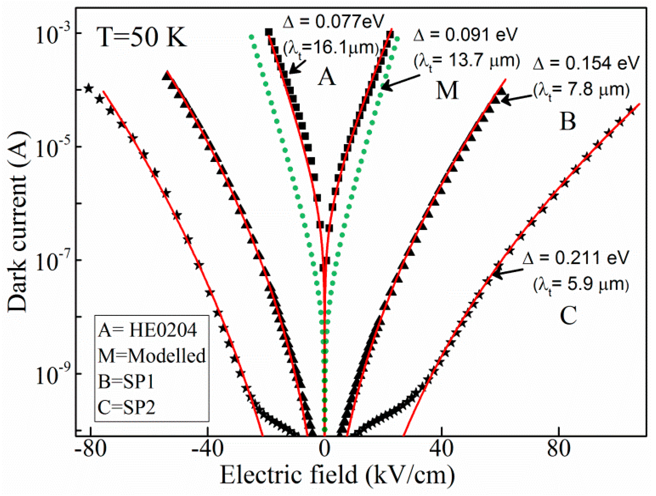
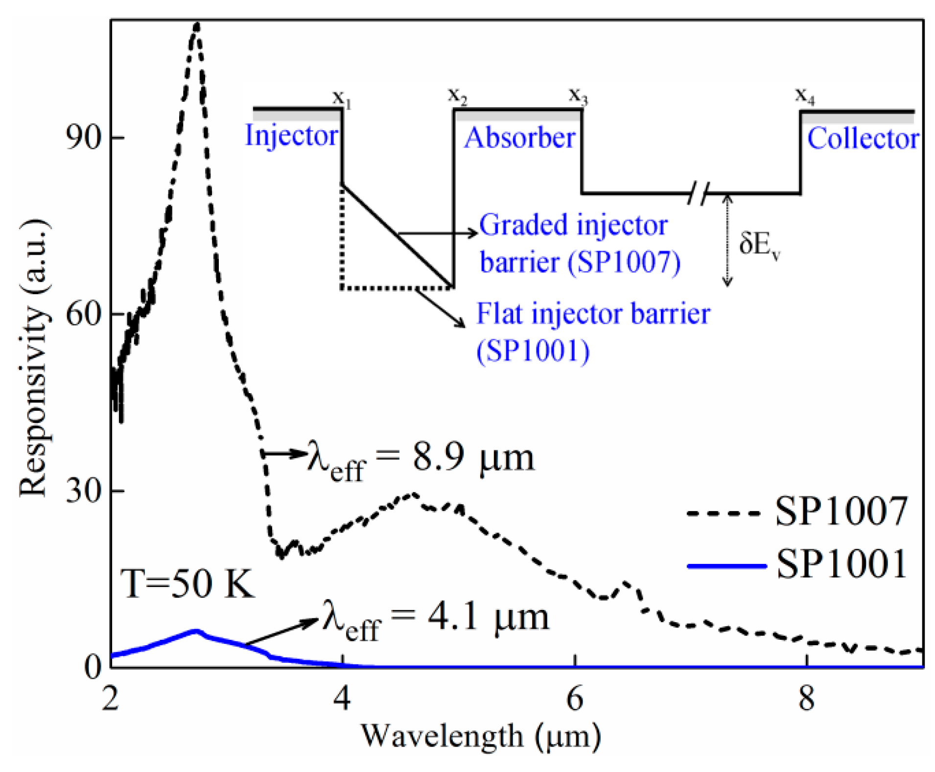
 )] and asymmetric [SP1007 ()] GaAs-based split-off IR sensors showing a clear difference in dark currents between the two structures. (b) The response spectra of SP1007 shows λeff = 8.9 μm (Δ′ = 0.139 eV) < Δ = 0.40 eV (λt = 3.1 μm) obtained from the dark current, whereas for SP1, λeff = 8.2 μm (Δ′ = 0.151 eV) matches with the value of Δ = 0.154 eV obtained from dark current fitting.
)] and asymmetric [SP1007 ()] GaAs-based split-off IR sensors showing a clear difference in dark currents between the two structures. (b) The response spectra of SP1007 shows λeff = 8.9 μm (Δ′ = 0.139 eV) < Δ = 0.40 eV (λt = 3.1 μm) obtained from the dark current, whereas for SP1, λeff = 8.2 μm (Δ′ = 0.151 eV) matches with the value of Δ = 0.154 eV obtained from dark current fitting.
)] and asymmetric [SP1007 ()] GaAs-based split-off IR sensors showing a clear difference in dark currents between the two structures. (b) The response spectra of SP1007 shows λeff = 8.9 μm (Δ′ = 0.139 eV) < Δ = 0.40 eV (λt = 3.1 μm) obtained from the dark current, whereas for SP1, λeff = 8.2 μm (Δ′ = 0.151 eV) matches with the value of Δ = 0.154 eV obtained from dark current fitting. ) and 15SP3 (), showing a clear difference in dark current for both structures for a similar λt. A dotted green (•••) line shows a simulated dark current of a modeled detector with Δ = 0.091 eV (λt = 13.7 μm). (b) D* for HE0204 and 15SP3, clearly showing a higher D* for 15SP3; the inset shows the response of HE0204, λeff = 16.1 μm (Δ′ = 0.077 eV) which was fitted to the dark current with Δ = 0.077 eV; for 15SP3, Δ′ (λeff) is 0.091 eV (13.7 μm) fitted to the dark current with Δ = 0.40 eV corresponding to λt = 3.1 μm.
) and 15SP3 (), showing a clear difference in dark current for both structures for a similar λt. A dotted green (•••) line shows a simulated dark current of a modeled detector with Δ = 0.091 eV (λt = 13.7 μm). (b) D* for HE0204 and 15SP3, clearly showing a higher D* for 15SP3; the inset shows the response of HE0204, λeff = 16.1 μm (Δ′ = 0.077 eV) which was fitted to the dark current with Δ = 0.077 eV; for 15SP3, Δ′ (λeff) is 0.091 eV (13.7 μm) fitted to the dark current with Δ = 0.40 eV corresponding to λt = 3.1 μm.
) and 15SP3 (), showing a clear difference in dark current for both structures for a similar λt. A dotted green (•••) line shows a simulated dark current of a modeled detector with Δ = 0.091 eV (λt = 13.7 μm). (b) D* for HE0204 and 15SP3, clearly showing a higher D* for 15SP3; the inset shows the response of HE0204, λeff = 16.1 μm (Δ′ = 0.077 eV) which was fitted to the dark current with Δ = 0.077 eV; for 15SP3, Δ′ (λeff) is 0.091 eV (13.7 μm) fitted to the dark current with Δ = 0.40 eV corresponding to λt = 3.1 μm.
 ) dots and empty (
 ) dots represent hot holes and cold holes in the absorber, and the green wavy arrow represents an incident photon with an energy exceeding Δ, whilst the red wavy arrow in the absorber shows an incident photon with an energy of Δ′. (b) Energy transfer via hot hole–cold hole interaction and the formation of a quasi-Fermi level (Efquasi) at a hot-hole temperature greater than the lattice temperature finally leads to the escape of hot holes from that Efquasi by the absorption of a long-wavelength photon, giving Δ′.
) dots and empty () dots represent hot holes and cold holes in the absorber, and the green wavy arrow represents an incident photon with an energy exceeding Δ, whilst the red wavy arrow in the absorber shows an incident photon with an energy of Δ′. (b) Energy transfer via hot hole–cold hole interaction and the formation of a quasi-Fermi level (Efquasi) at a hot-hole temperature greater than the lattice temperature finally leads to the escape of hot holes from that Efquasi by the absorption of a long-wavelength photon, giving Δ′.
) dots represent hot holes and cold holes in the absorber, and the green wavy arrow represents an incident photon with an energy exceeding Δ, whilst the red wavy arrow in the absorber shows an incident photon with an energy of Δ′. (b) Energy transfer via hot hole–cold hole interaction and the formation of a quasi-Fermi level (Efquasi) at a hot-hole temperature greater than the lattice temperature finally leads to the escape of hot holes from that Efquasi by the absorption of a long-wavelength photon, giving Δ′.
) dots and empty () dots represent hot holes and cold holes in the absorber, and the green wavy arrow represents an incident photon with an energy exceeding Δ, whilst the red wavy arrow in the absorber shows an incident photon with an energy of Δ′. (b) Energy transfer via hot hole–cold hole interaction and the formation of a quasi-Fermi level (Efquasi) at a hot-hole temperature greater than the lattice temperature finally leads to the escape of hot holes from that Efquasi by the absorption of a long-wavelength photon, giving Δ′.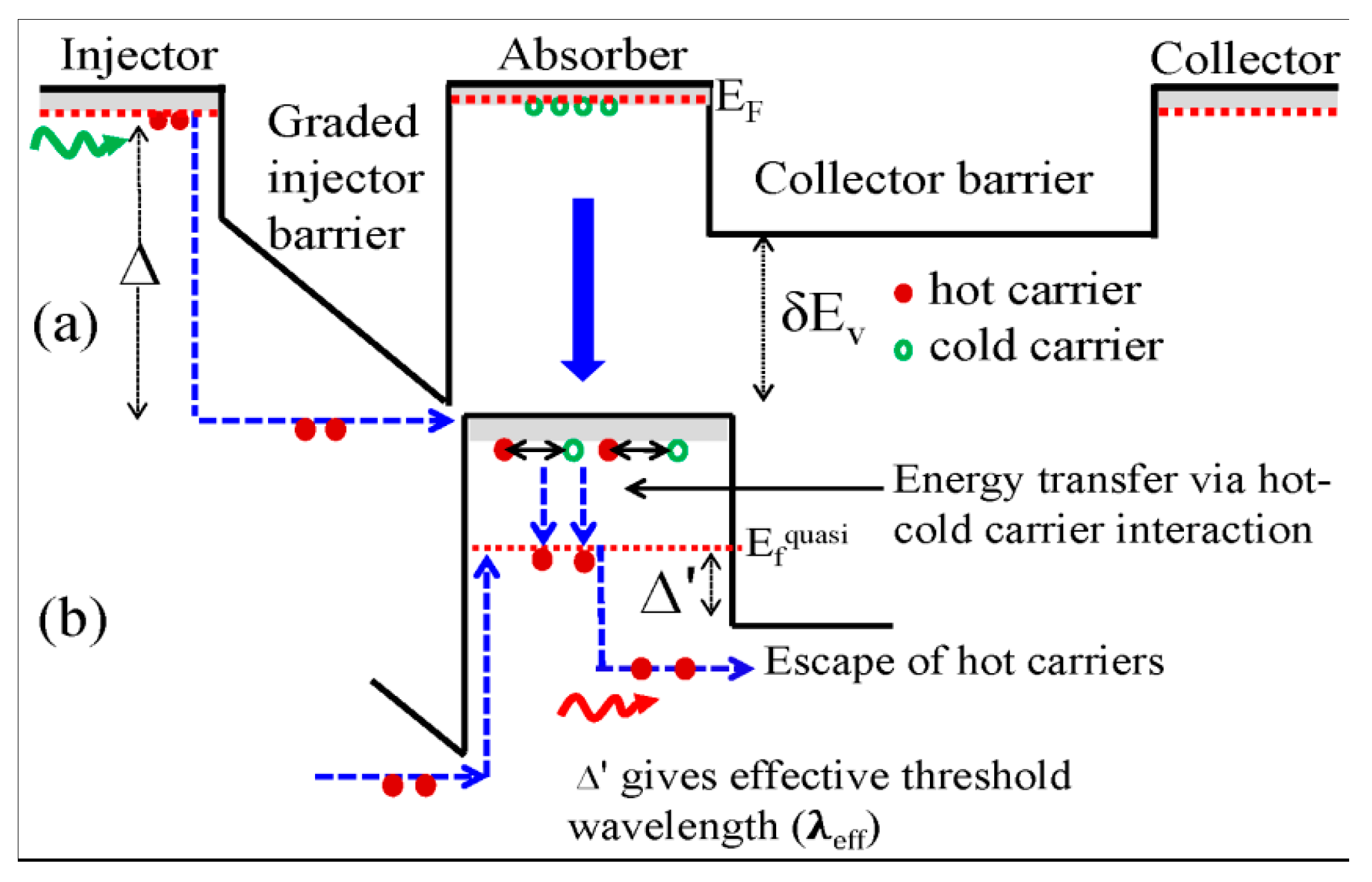


| No. | Sample | p-Doping (cm−3) | Al Mole Fraction x1 = x2 = x3 = x4 | Δ (eV) | λt (µm) | Δ′ (eV) | λeff (µm) | |||
|---|---|---|---|---|---|---|---|---|---|---|
| A | HE0204 | 1 × 10¹⁸ | 0.12 | 0.12 | 0.12 | 0.12 | 0.077 | 16.1 | 0.077 | 16.1 |
| M | Modeled | 1 × 10¹⁹ | 0.22 | 0.22 | 0.22 | 0.22 | 0.091 | 13.7 | 0.091 | 13.7 |
| B | SP1 | 3 × 10¹⁸ | 0.28 | 0.28 | 0.28 | 0.28 | 0.157 | 7.8 | 0.144 | 8.2 |
| C | SP2 | 3 × 10¹⁸ | 0.37 | 0.37 | 0.37 | 0.37 | 0.211 | 5.9 | 0.190 | 6.0 |
| D | LH1002 | 1 × 10¹⁹ | 0.57 | 0.57 | 0.57 | 0.57 | 0.30 | 4.13 | 0.295 | 4.2 |
| Sample | p-Doping (cm−3) | Al Mole Fraction | δEv (eV) | Δ (eV) | λt (μm) | Δ′ (eV) | λeff (μm) | |||
|---|---|---|---|---|---|---|---|---|---|---|
| x1 | x2 | x3 | x4 | |||||||
| SP1001 | 1 × 10¹⁹ | 0.75 | 0.75 | 0.57 | 0.57 | 0.10 | 0.40 0.40 | 3.1 3.1 | 0.302 0.034 | 4.1 at 50 K ~36 at 5.3 K |
| SP1007 | 1 × 10¹⁹ | 0.45 | 0.75 | 0.57 | 0.57 | 0.10 | 0.40 | 3.1 | 0.139 | 8.9 |
| 15SP3 | 1 × 10¹⁹ | 0.45 | 0.75 | 0.39 | 0.39 | 0.19 | 0.40 | 3.1 | 0.090 | 13.7 |
Disclaimer/Publisher’s Note: The statements, opinions and data contained in all publications are solely those of the individual author(s) and contributor(s) and not of MDPI and/or the editor(s). MDPI and/or the editor(s) disclaim responsibility for any injury to people or property resulting from any ideas, methods, instructions or products referred to in the content. |
© 2025 by the authors. Licensee MDPI, Basel, Switzerland. This article is an open access article distributed under the terms and conditions of the Creative Commons Attribution (CC BY) license (https://creativecommons.org/licenses/by/4.0/).
Share and Cite
Perera, A.G.U.; Lao, Y.; Jabegu, T.; Lei, S. Status of Extended Threshold Wavelength Split-Off Band IR Detectors and Quantum Material-Based Extension for Room-Temperature Operation. Micromachines 2025, 16, 286. https://doi.org/10.3390/mi16030286
Perera AGU, Lao Y, Jabegu T, Lei S. Status of Extended Threshold Wavelength Split-Off Band IR Detectors and Quantum Material-Based Extension for Room-Temperature Operation. Micromachines. 2025; 16(3):286. https://doi.org/10.3390/mi16030286
Chicago/Turabian StylePerera, A. G. Unil, Yanfeng Lao, Tara Jabegu, and Sidong Lei. 2025. "Status of Extended Threshold Wavelength Split-Off Band IR Detectors and Quantum Material-Based Extension for Room-Temperature Operation" Micromachines 16, no. 3: 286. https://doi.org/10.3390/mi16030286
APA StylePerera, A. G. U., Lao, Y., Jabegu, T., & Lei, S. (2025). Status of Extended Threshold Wavelength Split-Off Band IR Detectors and Quantum Material-Based Extension for Room-Temperature Operation. Micromachines, 16(3), 286. https://doi.org/10.3390/mi16030286