1. Introduction
RF MEMS attenuators have become the core passive components of high-frequency systems, such as 5G/6G communications, satellite payloads, and phased-array radars, by virtue of their low insertion loss, high linearity, and miniaturization [
1,
2,
3]. By dynamically adjusting signal attenuation, the device significantly extends the dynamic range in microwave test systems. It suppresses system saturation from strong signals while enhancing weak signal detection. Additionally, it protects front-end equipment with a blocking failure protection mechanism and optimizes impedance matching to reduce signal reflection and improve transmission efficiency. Furthermore, the attenuator effectively minimizes signal coupling and electromagnetic interference between multiple channels, thereby enhancing the testing accuracy of spectrum analyzers, vector network analyzers, and signal sources [
4,
5,
6,
7]. In practical applications, RF MEMS attenuators have been deeply integrated into military and civilian high-frequency systems. In the military field, they are widely used in radar systems [
8], satellite communications [
9], and multi-band communication networks [
10,
11,
12] to achieve reliable operation in complex electromagnetic environments by precisely controlling the signal power; in the civil field, their miniaturization and high-performance characteristics provide key support for 5G base stations, satellite Internet terminals and high-speed data links.
In contemporary RF/microwave systems, attenuators play a crucial role in signal power management, significantly influencing dynamic range, linearity, and stability. Traditional resistive attenuators offer simple structures and low costs but suffer from significant parasitic effects at high frequencies, reducing attenuation accuracy. PN-junction diode attenuators achieve continuous attenuation via bias voltage modulation of junction resistance, yet their limited power capacity and temperature sensitivity limit use in complex settings. FET digital attenuators facilitate rapid programmable control but face challenges related to conduction resistance and parasitic capacitance that impede their performance in wideband, high-precision applications. As communication technology advances toward higher frequencies, miniaturization, and intelligent integration, the drawbacks of traditional attenuators are more evident. MEMS-based switches offer a promising solution, using microfabrication to deeply integrate mechanical and electrical functions in attenuators. This yields devices with low insertion loss, high isolation, ultra-compactness, and outstanding linearity when paired with precision attenuation networks.
So far, researchers in the microwave field have carried out a great deal of research on attenuators. In 2017, Duy P. Nguyen et al. designed a monolithic microwave integrated circuit (MMIC) attenuator based on gallium arsenide FET technology, which for the first time employed two-dimensional stacked FETs in its structure. The results indicated that this step attenuator operated over a wide frequency range of 1.5~45 GHz, with an insertion loss ranging from 1.9 to 5.5 dB and a maximum attenuation of 26 dB [
13]. In 2021, Clifford D. Cheon et al. developed a DC~67 GHz step attenuator utilizing silicon–germanium bipolar complementary metal-oxide-semiconductor technology. This attenuator achieved an attenuation range of 31.5 dB with a step size of 0.5 dB and maintained an insertion loss below 7.8 dB [
14]. In 2022, Kim et al. designed a four-bit digital step attenuator operating within the frequency range of 0.5 to 12 GHz, achieving an attenuation coverage of up to 30 dB with an accuracy of 2 dB; the insertion loss varied between 2.8 and 8.3 dB while ensuring return loss was less than 12 dB [
15]. In addition, in 2024 Haipeng Fu et al. demonstrated a broadband high-linearity seven-bit digital step attenuator capable of delivering a remarkable attenuation range of up to 31.7 dB across the DC to 7 GHz frequency band; it featured minimum step accuracy at 0.25 dB and overall attenuation accuracy within 0.5 dB alongside an insertion loss better than or equal to 2.7 dB [
16]. At present, notable research gaps persist in RF MEMS attenuators. Key performance indicators like insertion loss, attenuation accuracy, return loss, and frequency coverage still fall short of the ideal. Balancing these performance aspects proves challenging, rendering simultaneous optimization unattainable. Further investigation is needed to optimize their microwave characteristics [
17,
18,
19,
20,
21].
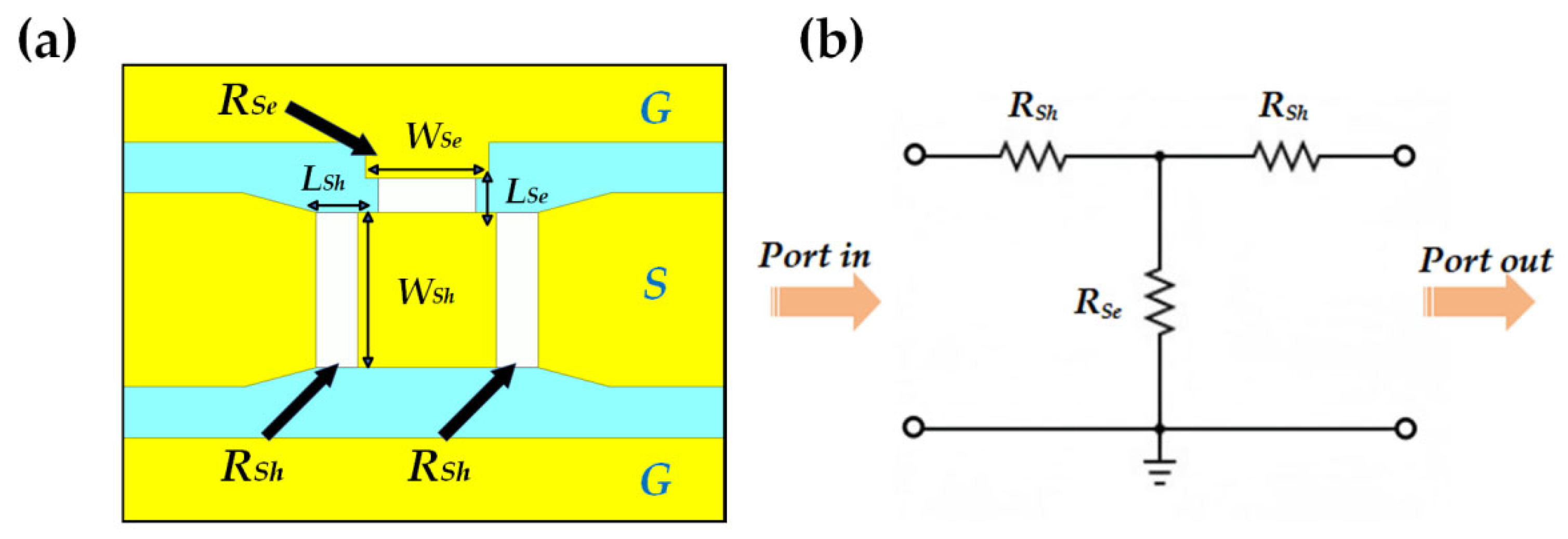
In this paper, a 3-bit MEMS digital attenuator is proposed. By combining the differentiated T-type attenuation network with the RF MEMS switches in the CPW, the attenuator not only reduces the process complexity, but also realizes the compact design of the device structure, which effectively improves the reliability and engineering realizability through the optimization of the number of switches under the premise of guaranteeing the function realization. In terms of performance, the attenuator can precisely regulate the reconfigurable attenuation value over a wide frequency range of DC-20 GHz, which significantly improves the attenuation accuracy. Meanwhile, through the optimization of impedance matching, the attenuator provides a solution with both high precision and flexibility for signal attenuation, and the attenuation can be dynamically adjusted according to the signal strength of the actual application, which can meet the needs of diversified systems.
3. Simulation
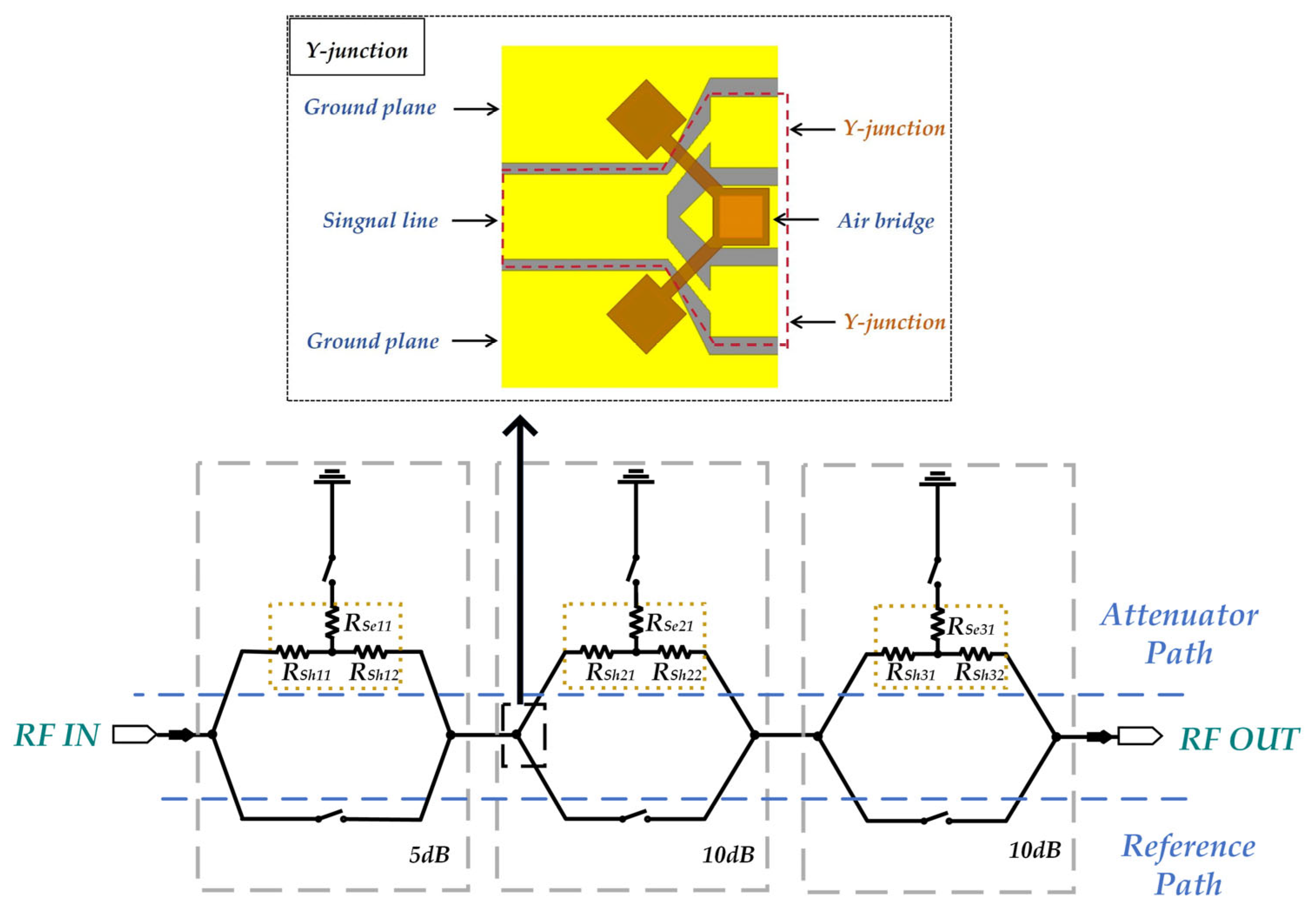
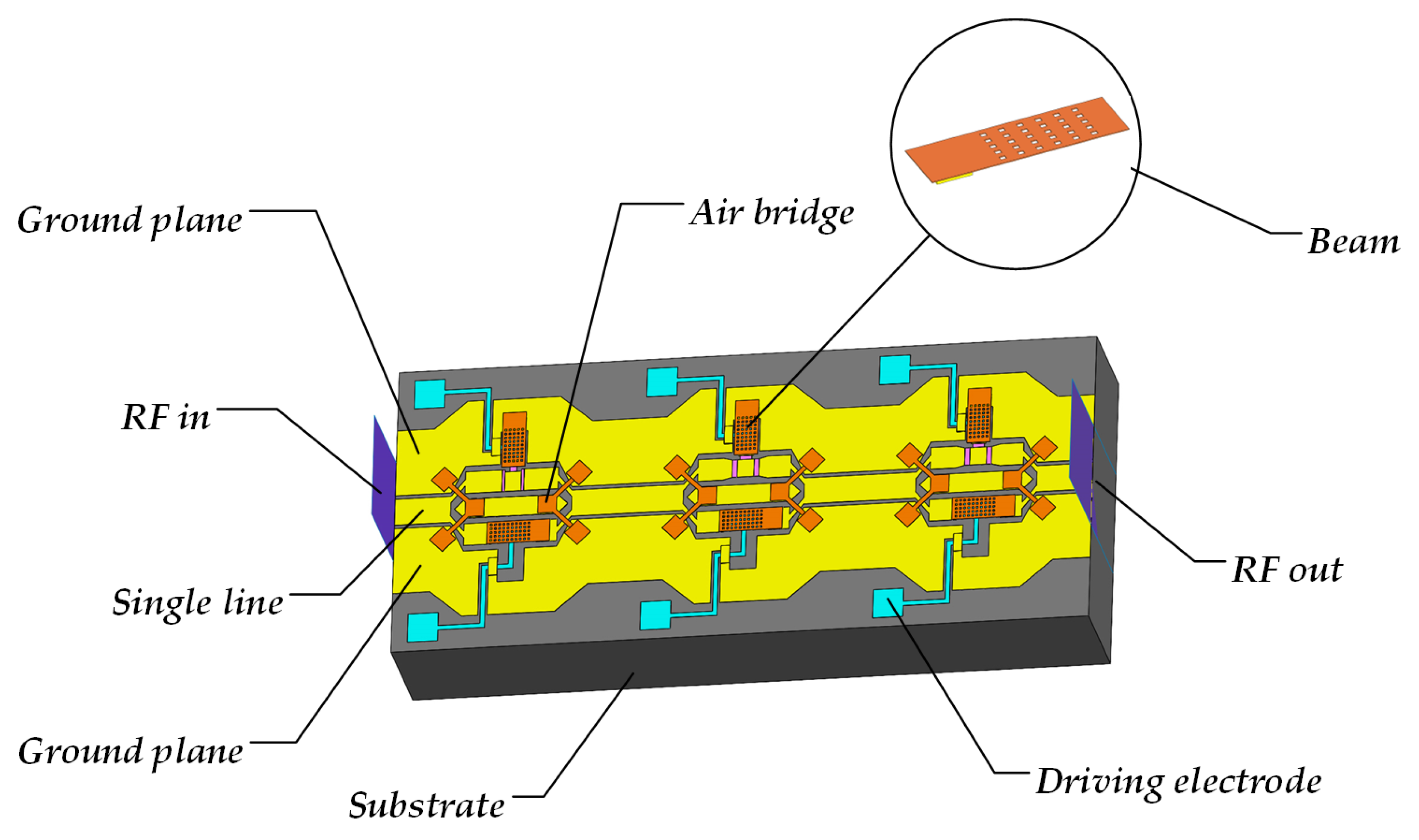
As shown in
Figure 6, a reconfigurable attenuator is designed by integrating resistor attenuation modules, RF MEMS switches, transmission lines, and power dividers. This attenuator consists of three attenuation bits (5 dB, 10 dB, and 10 dB) and is equipped with six RF MEMS switches to enable attenuation adjustment from 0 to 25 dB in steps of 5 dB. In the simulated structure, BF33 glass is selected as the substrate material owing to its low loss tangent (4.9 × 10
−6) and dielectric constant (4.6); gold (Au) is chosen for the air bridges, upper electrodes, and CPW components on account of its chemical stability and ease of fabrication in semiconductor processes. The resistor material is a 30 nm thick TaN thin film with a sheet resistance of 157 Ω/□. When the switches in the DC paths below each attenuation bit are turned on, the attenuator operates in the through mode (i.e., signal transmission without attenuation); conversely, when the switches in the attenuation network are activated, the attenuator enters the attenuation mode (i.e., signal attenuation according to the preset ratio).
Table 4 lists the main design parameters of this device.
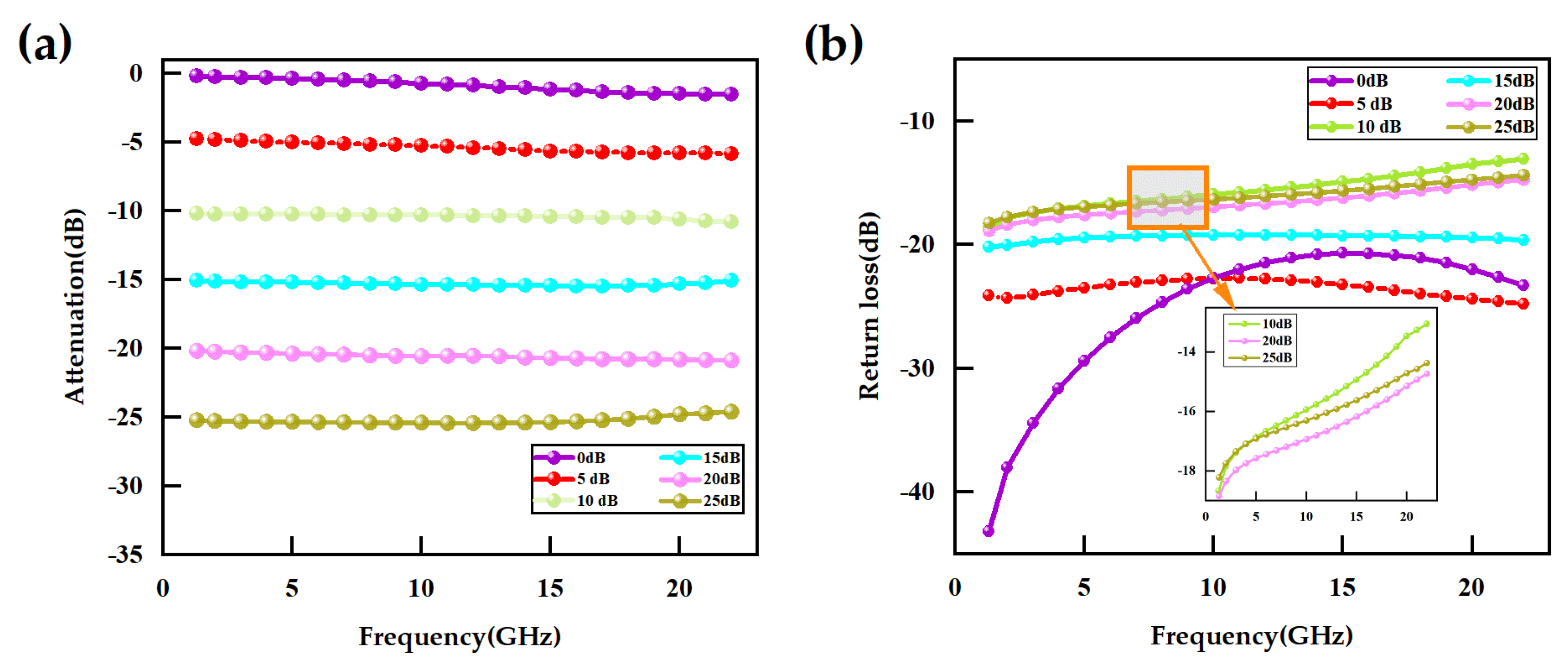
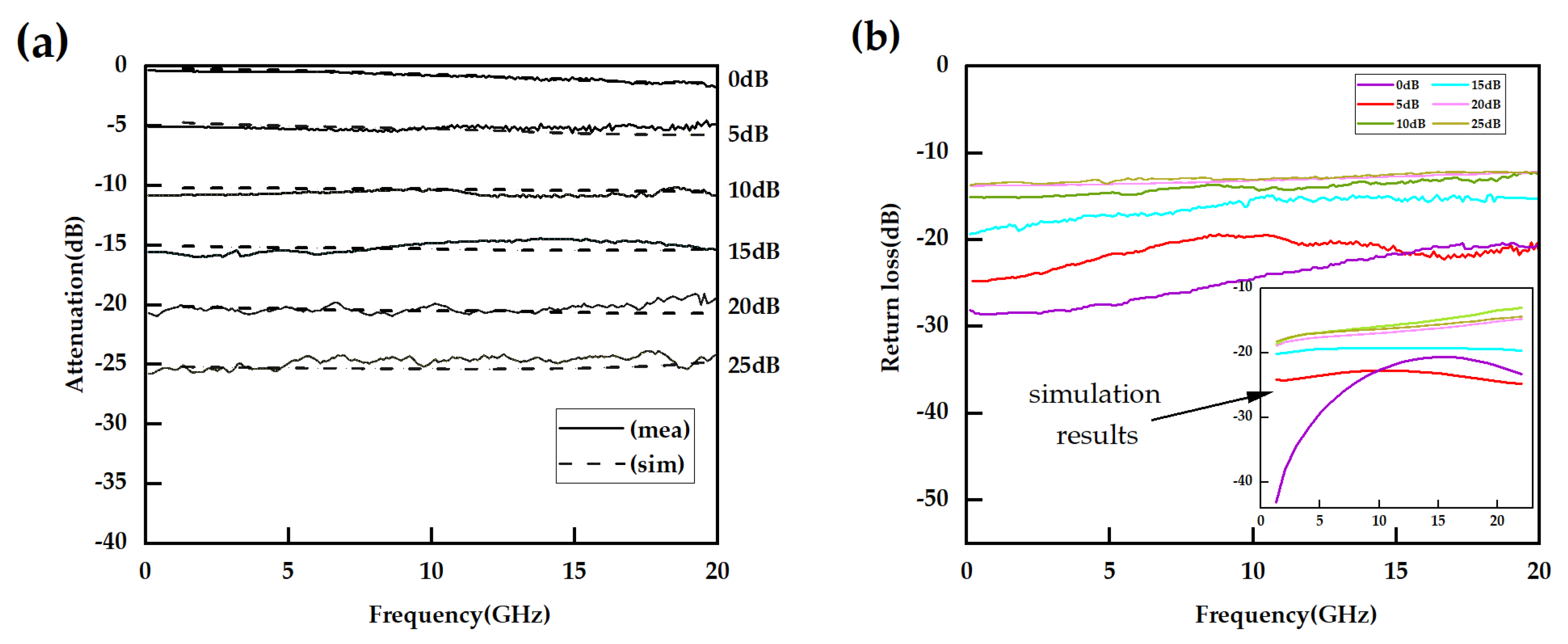
Systematic electromagnetic simulations were conducted using Ansys EM 2023 simulation software to evaluate the microwave performance of the attenuator. The results are presented in
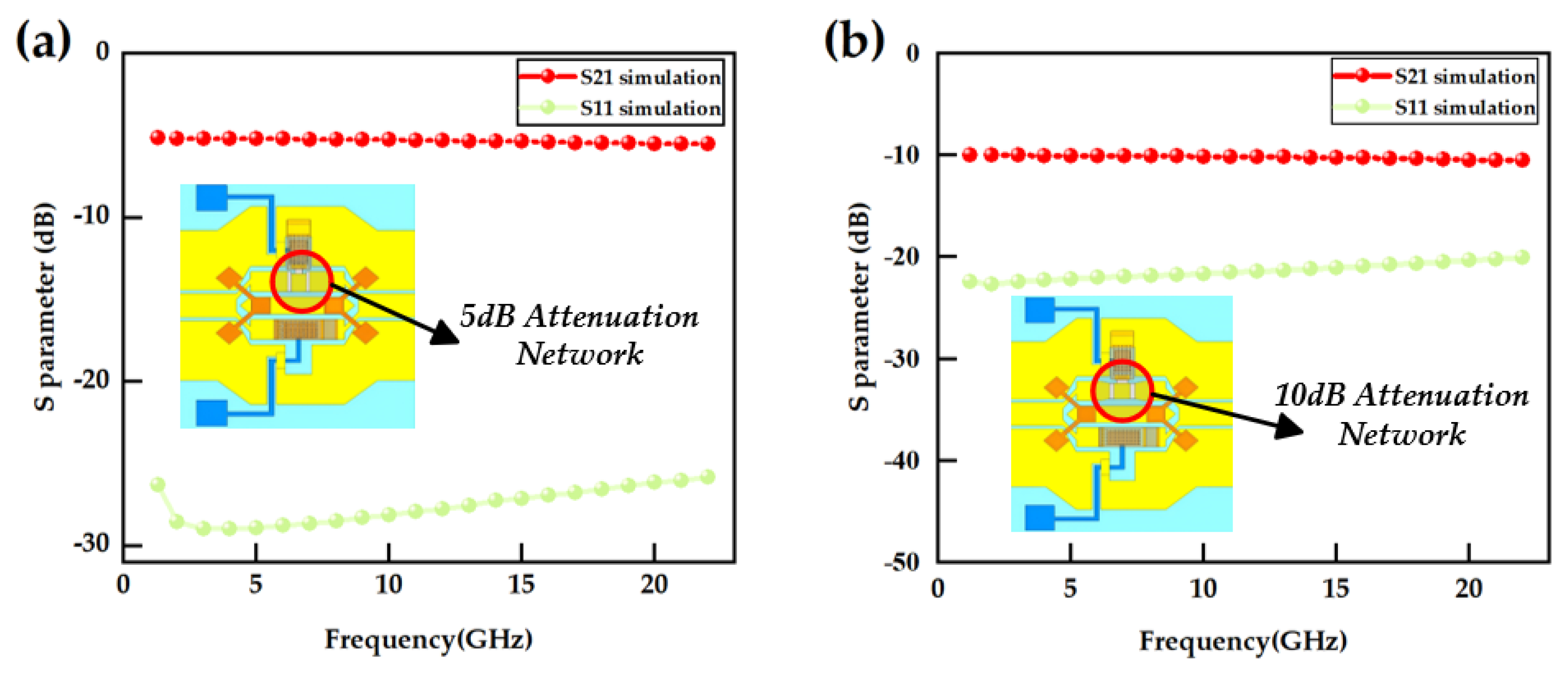
Figure 7. Simulation data for the 3-bit MEMS attenuator demonstrate that across the broad frequency range from DC to 20 GHz, key RF metrics such as attenuation accuracy and return loss remain within ideal ranges, fully validating its excellent RF performance and wideband applicability. The insertion loss of the attenuator is within 1.52 dB (0 dB mode). All attenuation states maintain an accuracy within 0.8 dB. Matching networks for all six attenuation states exhibit exceptional performance, with return loss exceeding 13.16 dB (VSWR < 1.56). The 15 dB state achieves the highest attenuation accuracy (<0.44 dB). The 5 dB state demonstrates the best return loss (>22.72 dB).
Compared to previous studies, this attenuator integrates a T-type TaN resistor network with MEMS switches, thereby achieving enhanced attenuation accuracy and a reduced device size while maintaining broadband performance and effective impedance matching. A summary of the detailed results is presented in
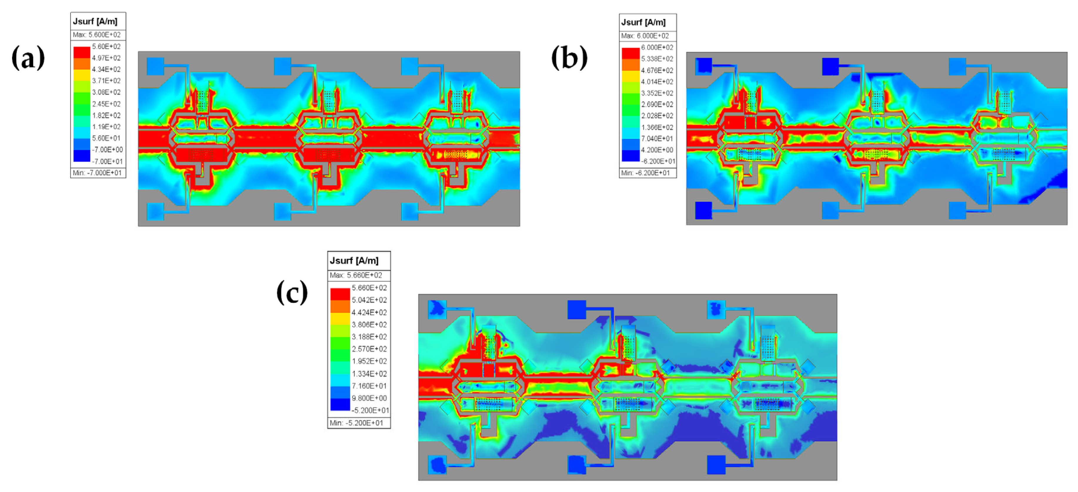
Table 5Given the multi-mode operational features of the attenuator, this study visually represents the optimized performance of a 3-bit attenuator by selecting three attenuation states: 0 dB, 15 dB, and 25 dB. Current density distribution maps (shown in
Figure 8) illustrate the electromagnetic characteristics and performance advantages across different operating modes. A gradient color scale differentiates current density levels within signal line areas. When the attenuation module is engaged, there is a significant reduction in current density, indicating that the attenuation network effectively degrades signals by absorbing electromagnetic wave energy, thus ensuring stable attenuation accuracy. In contrast, when the direct current path is activated, current density shows a uniform distribution; this indicates lossless signal transmission throughout the direct current pathway structure. This uniformity minimizes insertion loss while preserving signal integrity and suppressing hotspot formation as well as local overheating phenomena. These factors contribute to enhanced device reliability and long-term operational stability.
4. Processing and Manufacturing
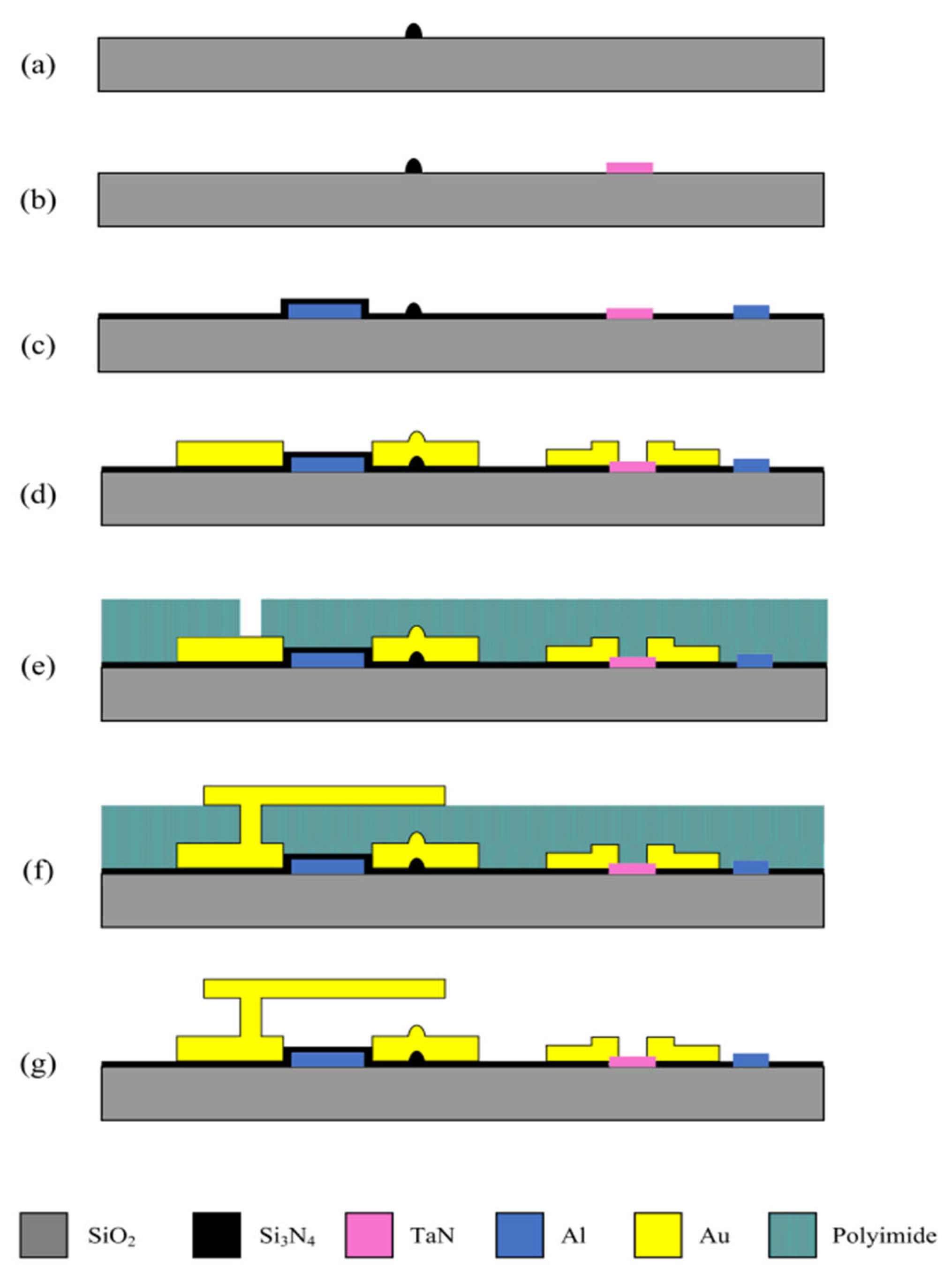
The 3-bit MEMS attenuator is manufactured using micro-nano surface technology, and the manufacturing process is schematically illustrated in
Figure 9, which includes seven steps as described below.
- (a)
A 400 nm thick silicon nitride (Si
4N
3) film was prepared using plasma-enhanced chemical vapor deposition (PECVD) technology, followed by reactive ion etching (RIE) to etch the film into a bump structure pattern, as shown in
Figure 9a.
- (b)
A 30 nm thick TaN film was deposited using magnetron sputtering as the resistive layer material. A metal dry etching process was used to prepare a TaN attenuation network on a glass substrate. The TaN resistive structure is shown in
Figure 9b.
- (c)
An ammonia–hydrogen peroxide mixed solution was used to etch the 640 nm thick aluminum (Al) layer deposited by sputtering to form the pull-down electrode structure. Concurrently, a 400 nm thick Si
4N
3 film was patterned using RIE to serve as a dielectric isolation layer between the drive electrode and the upper electrode, as well as a protective coating for the drive circuit, as shown in
Figure 9c.
- (d)
A titanium (Ti)/Au bilayer film, with a total thickness of 200 nm, was sputter-deposited to serve as a seed layer. This bilayer comprises a 50 nm thick titanium layer and a 150 nm thick gold layer. An electroplating mold was subsequently prepared using a 6.7-μm AZ4620 photoresist through a photolithography process. Following this, a 1.28-μm gold layer was electroplated to create the CPW structure. The excess seed layer was then eliminated via an ion beam etching (IBE) dry etching process, yielding the final CPW structure as depicted in
Figure 9d.
- (e)
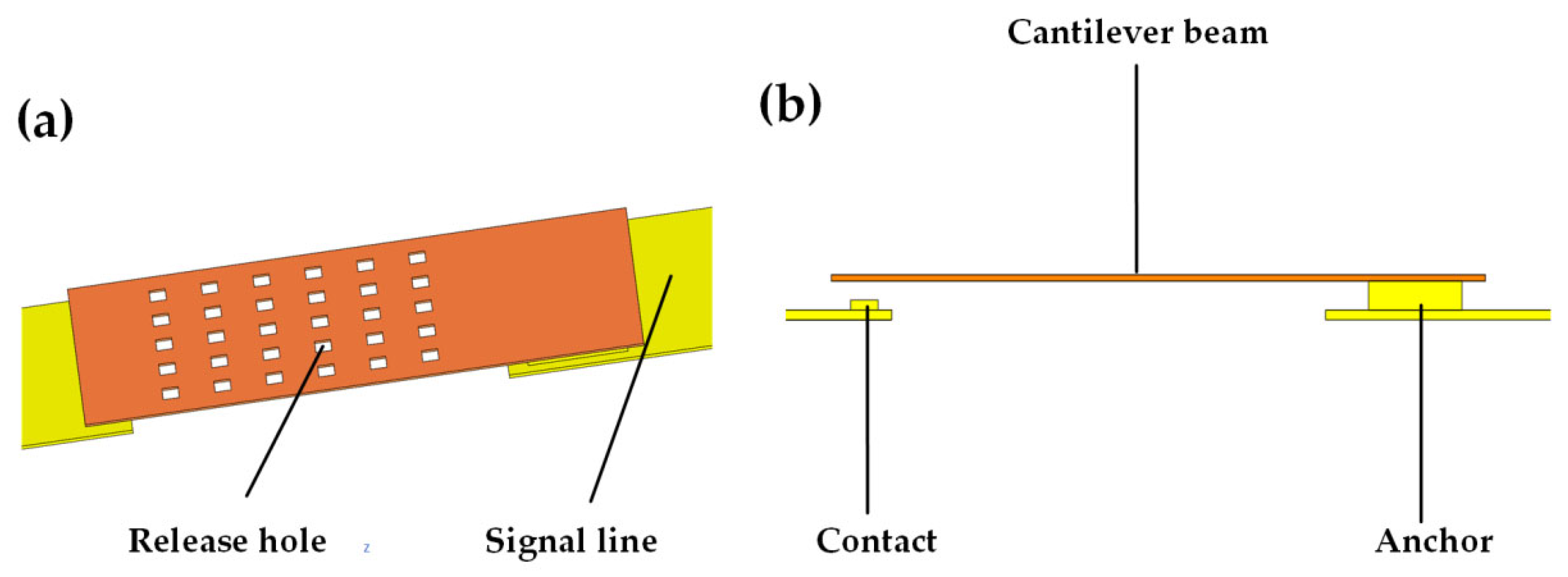
Polyimide is uniformly spin-coated onto the wafer. Following a pre-curing process and subsequent curing at elevated temperatures, A 2-μm thin film is formed to act as the sacrificial layer for the cantilever beam. The anchor point area of the cantilever beam is then etched using RIE during the photolithography process, as illustrated in
Figure 9e.
- (f)
A 150 nm Au layer was sputter-deposited onto the cured polyimide wafer as a seed layer. An electroplating mold was then prepared using a 6.7-μm AZ4620 photoresist through photolithography. Next, a 1.28-μm gold layer was electroplated to form the upper electrode of the cantilever beam. The remaining seed layer was removed via IBE, resulting in the cantilever beam structure shown in
Figure 9f.
- (g)
Oxygen plasma dry etching is utilized to precisely remove the polyimide sacrificial layer, enabling the release of the device. Given that this process operates under high-temperature conditions, it is crucial to control the release time per cycle to avoid excessive duration, which could otherwise lead to warping of the top electrode. To ensure the complete elimination of the sacrificial layer, multiple cycles are necessary, as demonstrated in
Figure 9g.
Figure 9.
Device Process Flow Chart: (a) Fabricate contacts; (b) Fabricate resistor networks; (c) Fabricate driving electrodes; (d) Fabricate CPW; (e) Fabricate anchor points; (f) Fabricate cantilevers; (g) Release sacrificial layers.
Figure 9.
Device Process Flow Chart: (a) Fabricate contacts; (b) Fabricate resistor networks; (c) Fabricate driving electrodes; (d) Fabricate CPW; (e) Fabricate anchor points; (f) Fabricate cantilevers; (g) Release sacrificial layers.
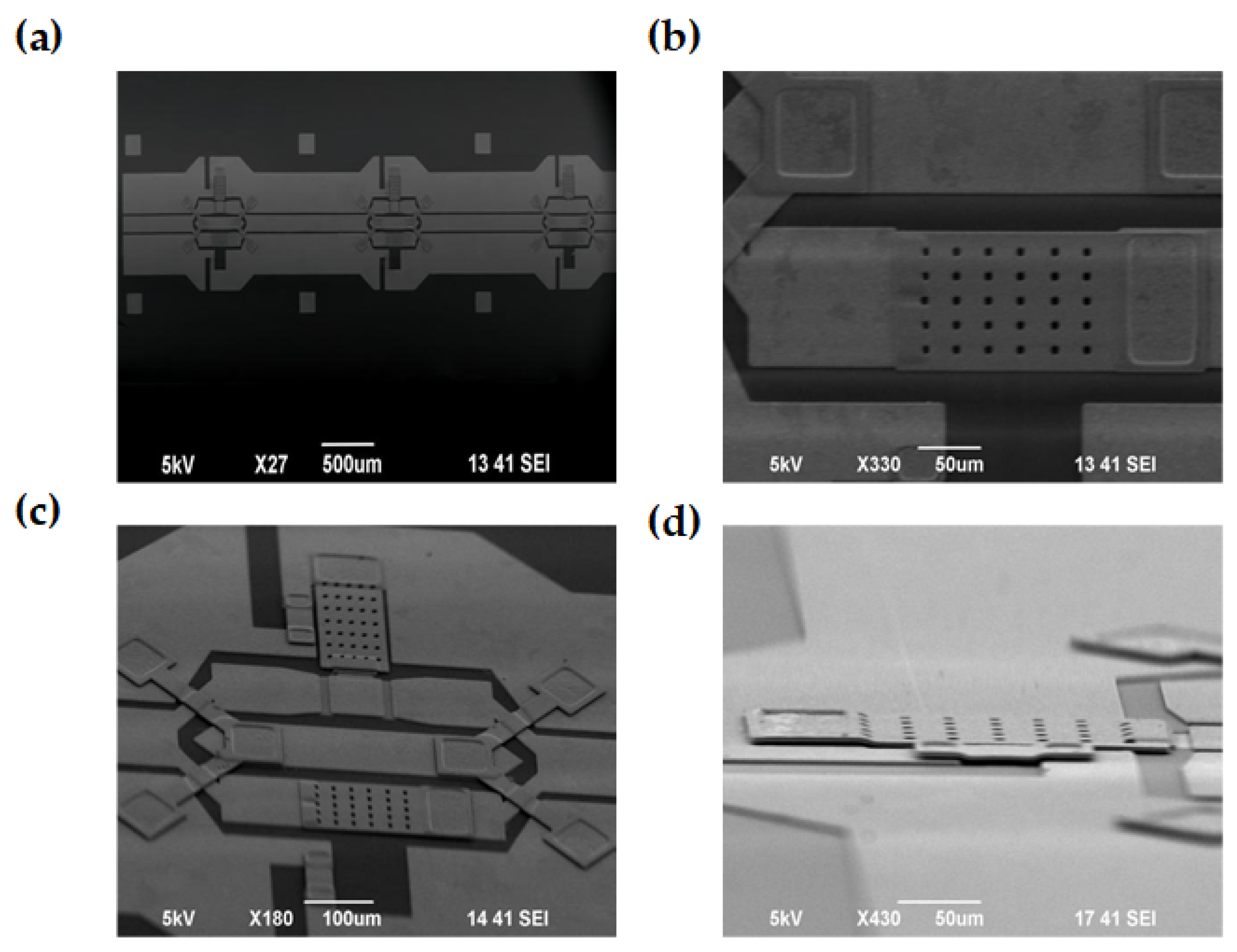
The physical sample is depicted in
Figure 10, showcasing a successfully fabricated 3-bit reconfigurable attenuator. In
Figure 10a, the overall structure of the 3-bit attenuator is characterized using high-resolution scanning electron microscopy (SEM), which clearly reveals the microscopic morphology of the device along with the integrated layout of its functional modules.
Figure 10b–d provide detailed illustrations of the local structures pertaining to the MEMS switch, T-type attenuator network, and Y-type power distributor, each exhibiting distinct geometric contours and excellent processing accuracy. This validates the feasibility of the proposed design scheme.
