
Wafer Level Vacuum Packaging of MEMS-Based Uncooled Infrared Sensors


Abstract
1. Introduction
2. Experimental
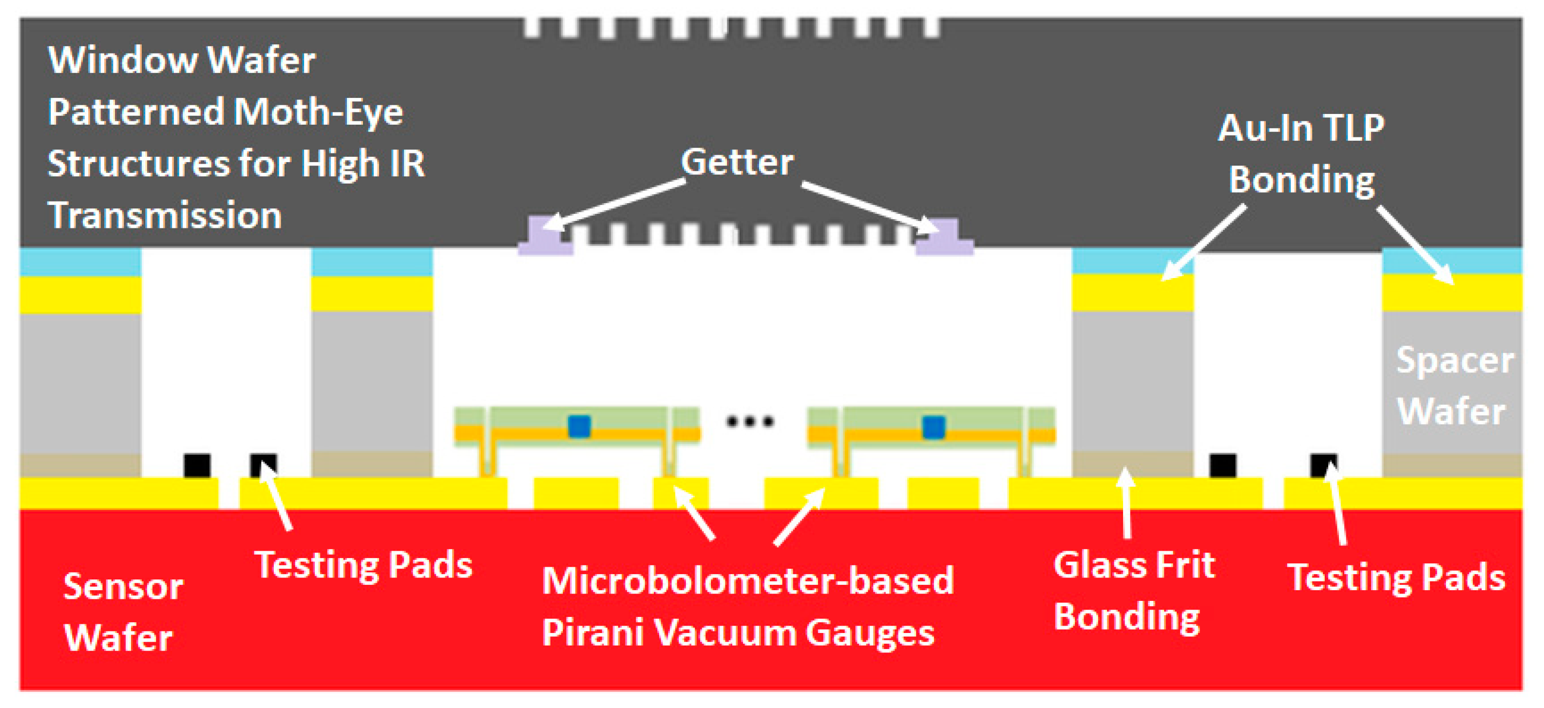
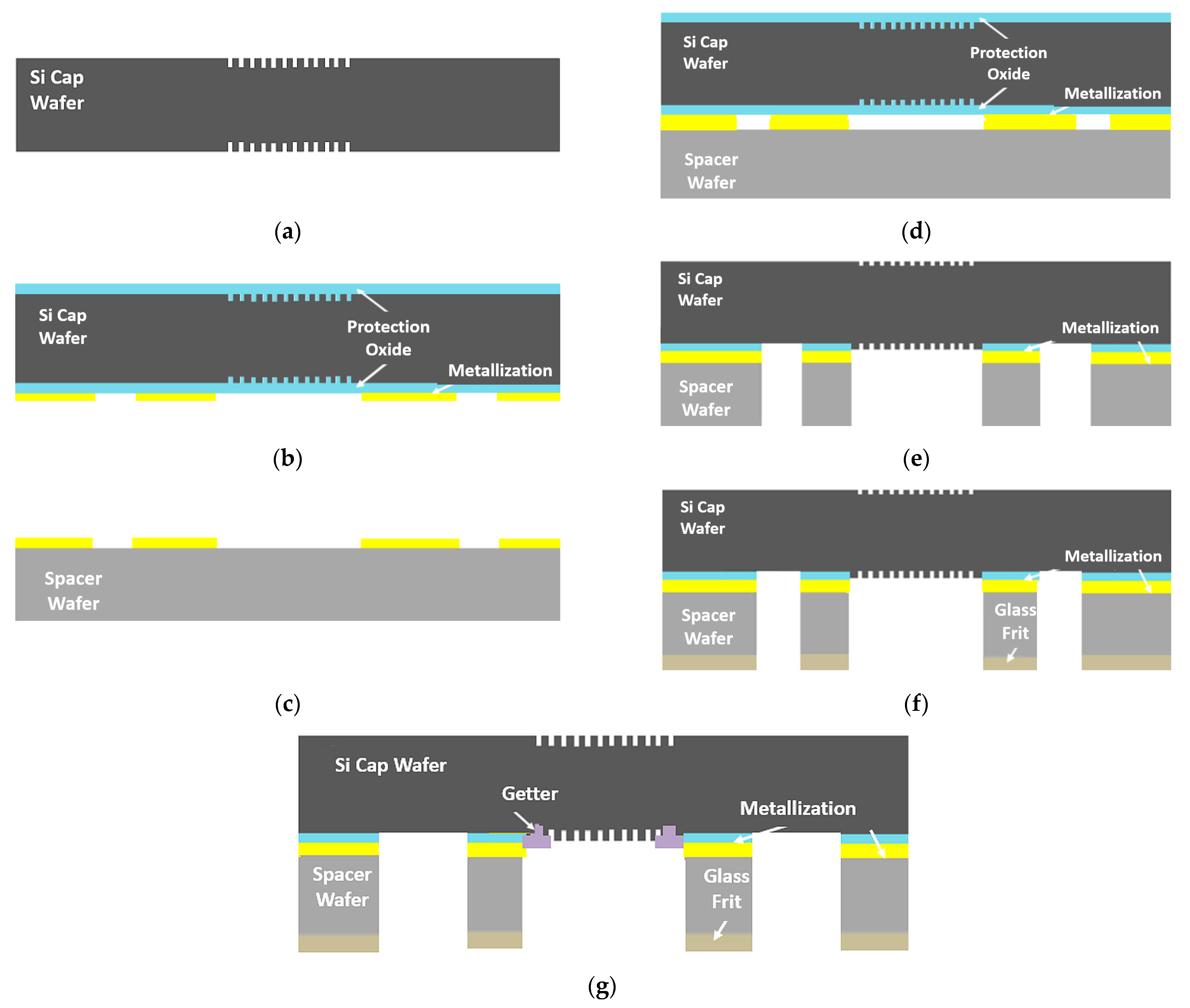
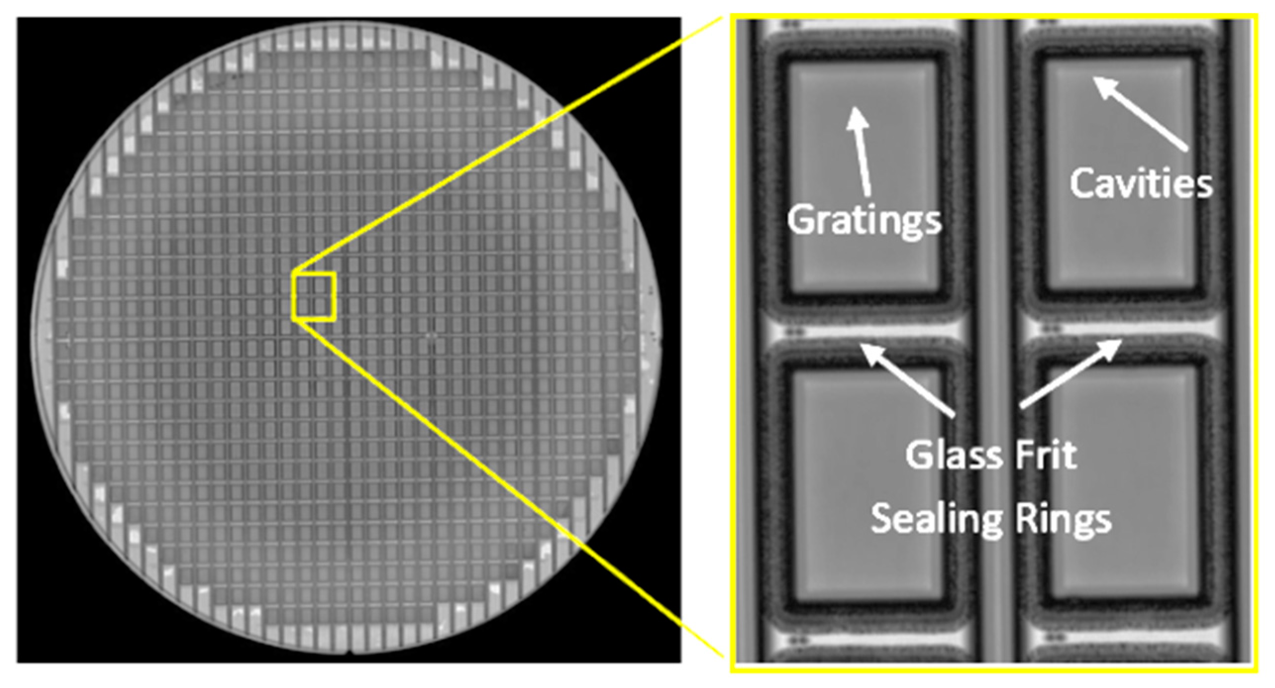
2.1. Proposed Cap Wafer Fabrication Approach
2.2. Fabrication Processes
3. Results & Discussion
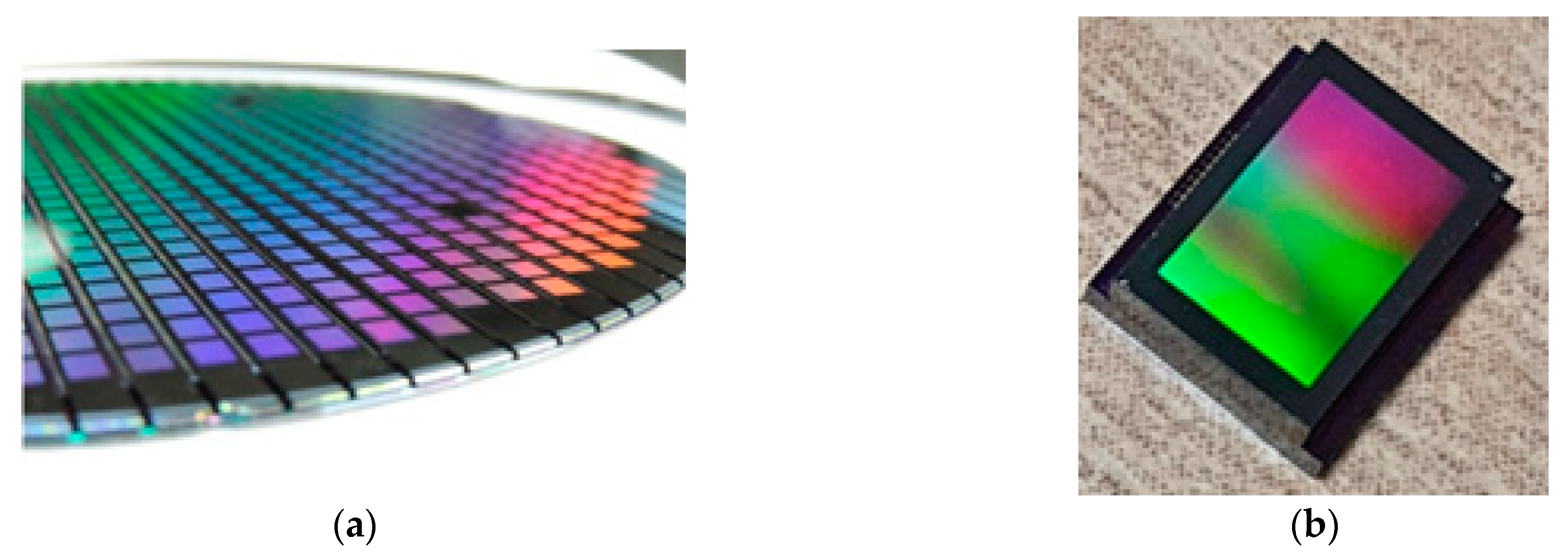
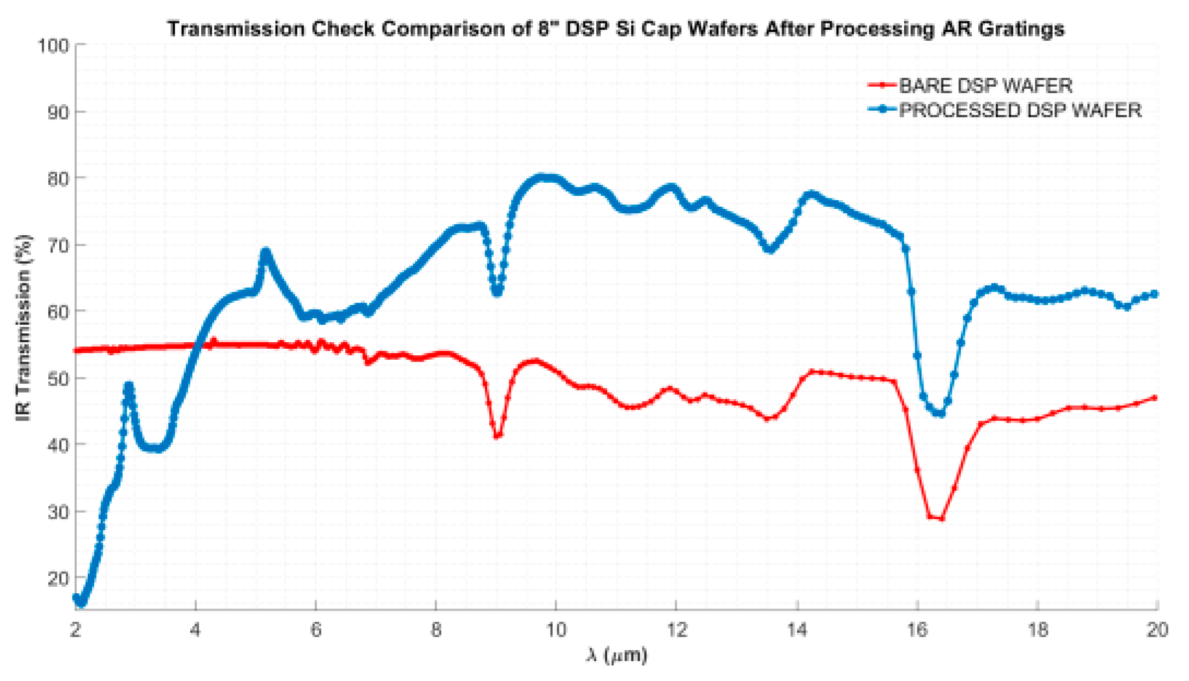
3.1. Transmission Behavior of Double-Side Anti-Reflection Moth Eye (Grating) Structures
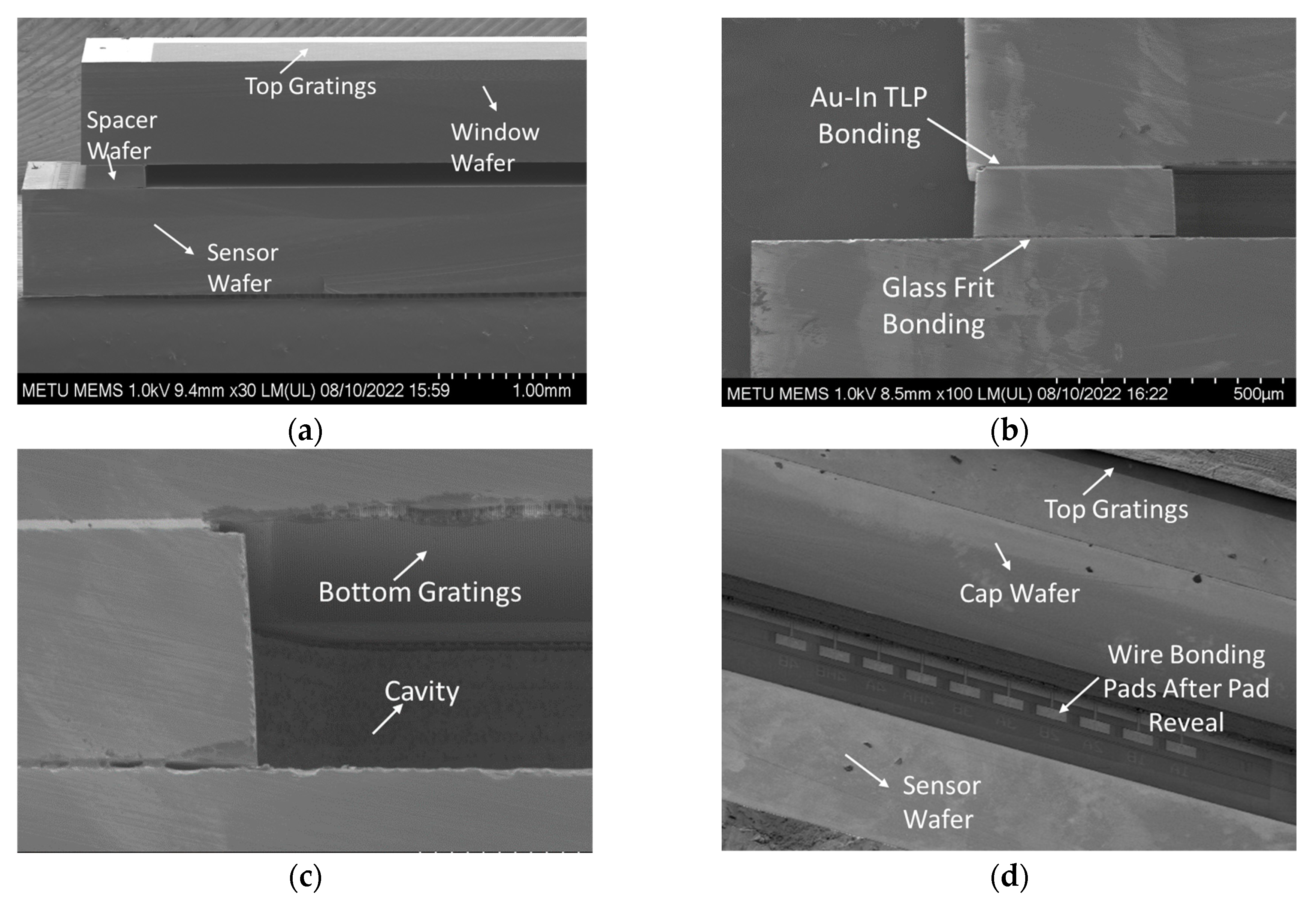
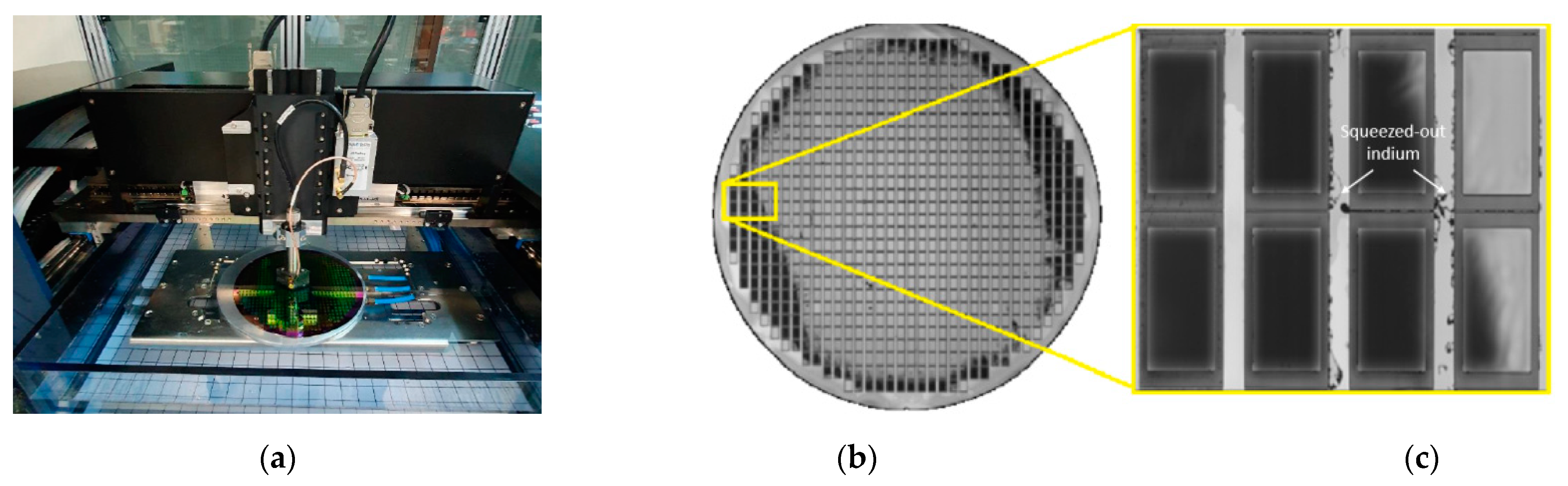
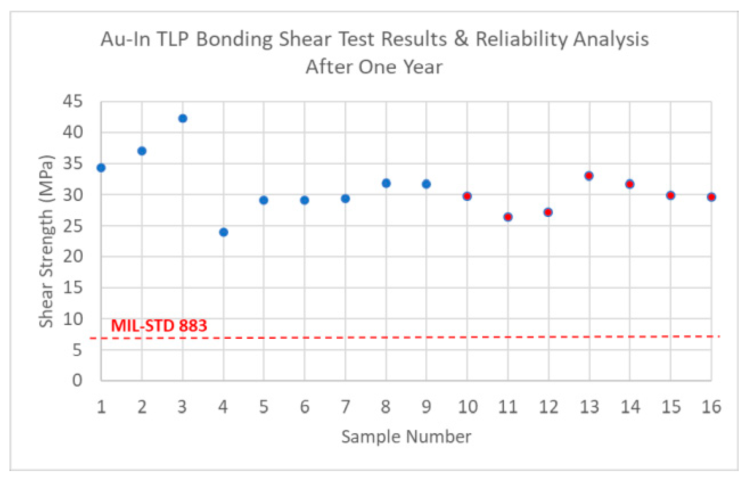
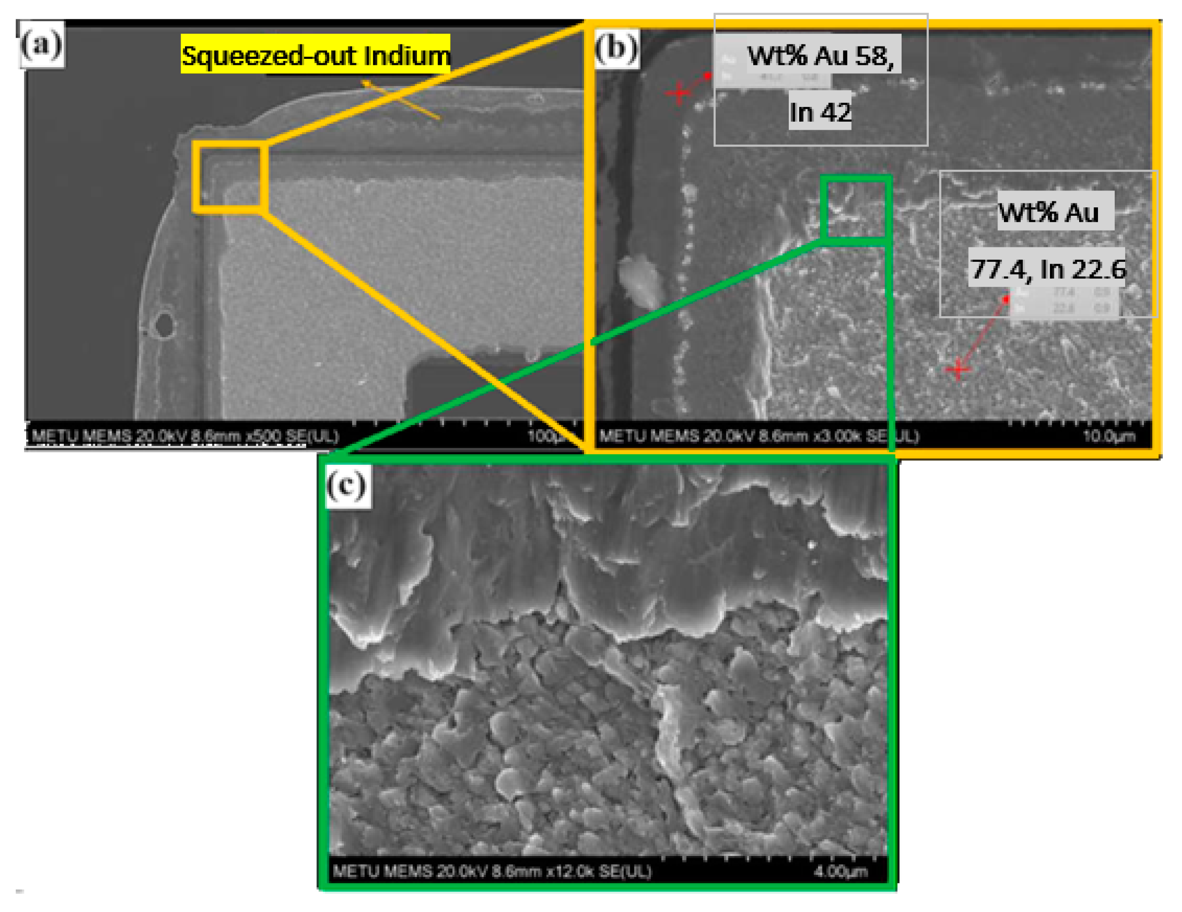
3.2. Au-In TLP Bonding Quality
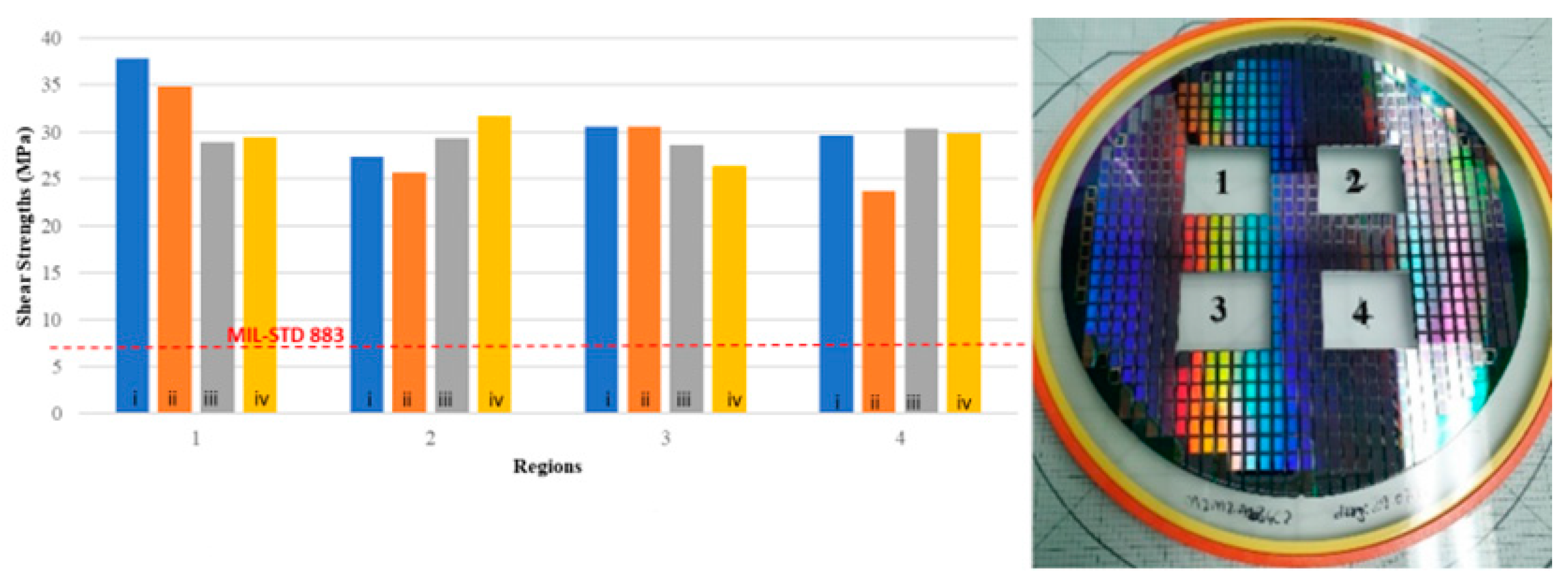
3.3. Glass Frit Bonding Quality
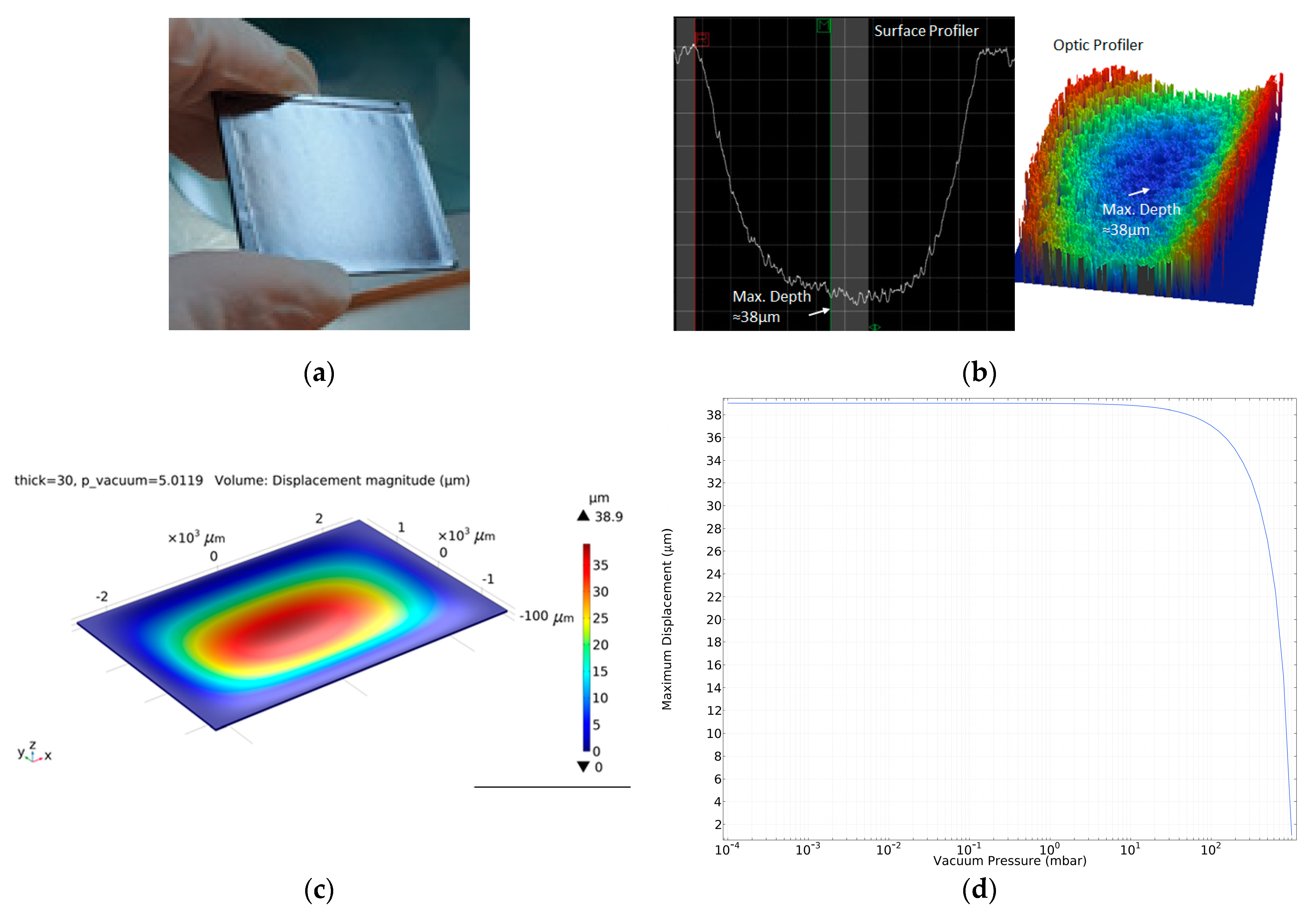
3.4. Hermeticity Tests of the Proposed Cap Wafer Fabrication Method
4. Conclusions
Author Contributions
Funding
Data Availability Statement
Acknowledgments
Conflicts of Interest
References
- Hsieh, C.T.; Ting, J.-M.; Yang, C.; Chung, C.K. The introduction of MEMS packaging technology. In Proceedings of the 4th International Symposium on Electronic Materials and Packaging, Kaohsiung, Taiwan, 4–6 December 2002; pp. 300–306. [Google Scholar] [CrossRef]
- Kimata, M.; Tokuda, T.; Tsuchinaga, A.; Matsumura, T.; Abe, H.; Tokashiki, N. Vacuum Packaging Technology for Uncooled Infrared Sensor. IEEJ Trans. Electr. Electron. Eng. 2010, 5, 175–180. [Google Scholar] [CrossRef]
- Ramm, P.; Lu, J.J.Q.; Taklo, M.M.V. Handbook of Wafer Bonding, 1st ed.; Wiley-VCH Verlag GmbH & Co.KGaA: Weinheim, Germany, 2012. [Google Scholar]
- Chae, J.; Giachino, J.M.; Najafi, K. Fabrication and Characterization of a Wafer-Level MEMS Vacuum Package with Vertical Feedthroughs. J. Microelectromech. Syst. 2008, 17, 193–200. [Google Scholar] [CrossRef]
- Demirhan Aydın, G. Wafer Level Vacuum Packaging Technology for MEMS Based Long-Wave Infrared Sensors. Ph.D. Thesis, Middle East Technical University, Ankara, Turkey, 2022. [Google Scholar]
- Stenchly, V.; Lofink, F.; Reinert, W. AR-concepts for hermetic wafer level packaging of uncooled FIR bolometer arrays. In Proceedings of the 5th Electronics System-integration Technology Conference (ESTC), Helsinki, Finland, 16–18 September 2014. [Google Scholar] [CrossRef]
- Hilton, A.; Temple, D.; Lannon, J.; Schimert, T.R.; Skidmore, G.; Gooch, R.; Trujillo, C.; Miskimins, S.; Li, C. Wafer-Level Vacuum Packaging of Microbolometer-Based Infrared Imagers. In Proceedings of the International Wafer-Level Packaging Conference, San Jose, CA, USA, 18–20 October 2016. [Google Scholar]
- Li, Q.; Goosen, H.; van Keulen, F.; van Beek, J.; Zhang, G. Assessment of testing methodologies for thin-film vacuum MEMS packages. Microsyst. Technol. 2008, 15, 161–168. [Google Scholar] [CrossRef]
- Candler, R.N.; Park, W.-T.; Li, H.; Yama, G.; Partridge, A.; Lutz, M.; Kenny, T. Single wafer encapsulation of mems devices. IEEE Trans. Adv. Packag. 2003, 26, 227–232. [Google Scholar] [CrossRef]
- Stark, B.; Najafi, K. A Low-Temperature Thin-Film Electroplated Metal Vacuum Package. J. Microelectromech. Syst. 2004, 13, 147–157. [Google Scholar] [CrossRef]
- Stark, B.H. Thin Film Technologies for Hermetic and Vacuum Packaging of MEMS; University of Michigan: Ann Arbor, MI, USA, 2004. [Google Scholar]
- Go, J.S.; Cho, Y.-H. Experimental evaluation of anodic bonding process using Taguchi method for maximum interfacial fracture toughness. In Proceedings of the Eleventh Annual International Workshop on Micro Electro Mechanical Systems. An Investigation of Micro Structures, Sensors, Actuators, Machines and Systems (Cat. No.98CH36176), Heidelberg, Germany, 25–29 January 1998; pp. 318–321. [Google Scholar] [CrossRef]
- Tanaka, S. Wafer-level hermetic MEMS packaging by anodic bonding and its reliability issues. Microelectron. Reliab. 2014, 54, 875–881. [Google Scholar] [CrossRef]
- Plößl, A.; Kräuter, G. Wafer direct bonding: Tailoring adhesion between brittle materials. Mater. Sci. Eng. R Rep. 1999, 25, 1–88. [Google Scholar] [CrossRef]
- Dragoi, V.; Mittendorfer, G.; Thanner, C.; Lindner, P. Wafer-level plasma activated bonding: New technology for MEMS fabrication. Microsyst. Technol. 2007, 14, 509–515. [Google Scholar] [CrossRef]
- Takagi, H.; Maeda, R. Aligned room-temperature bonding of silicon wafers in vacuum by argon beam surface activation. J. Micromech. Microeng. 2004, 15, 290–295. [Google Scholar] [CrossRef]
- Kim, J.; Kim, I.; Choi, Y.; Paik, K.-W. Studies on the polymer adhesive wafer bonding method using photo-patternable materials for MEMS motion sensors applications. IEEE Trans. Compon. Packag. Manuf. Technol. 2012, 2, 1118–1127. [Google Scholar] [CrossRef]
- Bleiker, S.; Dubois, V.; Schröder, S.; Stemme, G.; Niklaus, F. Adhesive wafer bonding with ultra-thin intermediate polymer layers. Sens. Actuators A Phys. 2017, 260, 16–23. [Google Scholar] [CrossRef]
- Yun, C.H.; Martin, J.; Chen, L.; Frey, T.J. Clean and Conductive Wafer Bonding for MEMS. ECS Trans. 2008, 16, 117–124. [Google Scholar] [CrossRef]
- Xu, D.; Jing, E.; Xiong, B.; Wang, Y. Wafer-level vacuum packaging of micromachined thermoelectric IR sensors. IEEE Trans. Adv. Packag. 2010, 33, 904–911. [Google Scholar] [CrossRef]
- Yun, C.; Martin, J.; Tarvin, E.; Winbigler, J. AL to AL wafer bonding for MEMS encapsulation and 3-D interconnect. In Proceedings of the 2008 IEEE 21st International Conference on Micro Electro Mechanical Systems, Tucson, AZ, USA, 13–17 January 2008; pp. 810–813. [Google Scholar] [CrossRef]
- Deillon, L.; Hessler-Wyser, A.; Hessler, T.; Rappaz, M. Solid-liquid interdiffusion (SLID) bonding in the Au–In system: Experimental study and 1D modelling. J. Micromech. Microeng. 2015, 25, 125016. [Google Scholar] [CrossRef]
- Yoon, S.W.; Glover, M.D.; Shiozaki, K. Nickel–Tin Transient Liquid Phase Bonding Toward High-Temperature Operational Power Electronics in Electrified Vehicles. IEEE Trans. Power Electron. 2012, 28, 2448–2456. [Google Scholar] [CrossRef]
- Temel, O. Investigation of Solder Materials and Bond Formation for Wafer Level Packaging of MEMS Devices. Ph.D. Thesis, METU, Ankara, Turkey, 2020. [Google Scholar]
- Welch, W.C.; Najafi, K. Nickel-Tin Transient Liquid Phase (TLP) Wafer Bonding for MEMS Vacuum Packaging. In Proceedings of the TRANSDUCERS 2007—2007 International Solid-State Sensors, Actuators and Microsystems Conference, Lyon, France, 10–14 June 2007. [Google Scholar] [CrossRef]
- Sohn, Y.-C.; Wang, Q.; Ham, S.-J.; Jeong, B.-G.; Jung, K.-D.; Choi, M.-S.; Kim, W.-B.; Moon, C.-Y. Wafer-level low temperature bonding with Au-In system. In Proceedings of the 57th Electronic Components and Technology Conference, Sparks, NV, USA, 29 May 2007–1 June 2007; pp. 633–637. [Google Scholar] [CrossRef]
- Xu, H.; Suni, T.; Vuorinen, V.; Li, J.; Heikkinen, H.; Monnoyer, P.; Paulasto-Kröckel, M. Wafer-level SLID bonding for MEMS encapsulation. Adv. Manuf. 2013, 1, 226–235. [Google Scholar] [CrossRef]
- Chidambaram, V.; Bangtao, C.; Lip, G.C.; Woo, D.R.M. Au-In-based hermetic sealing for MEMS packaging for down-hole application. J. Electron. Mater. 2014, 43, 2498–2509. [Google Scholar] [CrossRef]
- Rautiainen, A.; Vuorinen, V.; Heikkinen, H.; Paulasto-Krockel, M. Wafer-Level AuSn/Pt Solid–Liquid Interdiffusion Bonding. IEEE Trans. Compon. Packag. Manuf. Technol. 2018, 8, 169–176. [Google Scholar] [CrossRef]
- Sood, S.; Farrens, S.; Pinker, R.; Xie, J.; Cataby, W. Al-Ge Eutectic Wafer Bonding and Bond Characterization for CMOS Compatible Wafer Packaging. ECS Trans. 2010, 33, 93–101. [Google Scholar] [CrossRef]
- Knechtel, R. Glass frit bonding: An universal technology for wafer level encapsulation and packaging. Microsyst. Technol. 2005, 12, 63–68. [Google Scholar] [CrossRef]
- Sun, Z.; Pan, D.; Wei, J.; Wong, C.K. Ceramics Bonding Using Solder Glass Frit. J. Electron. Mater. 2004, 33, 1516–1523. [Google Scholar] [CrossRef]
- Knechtel, R.; Wiemer, M.; Frömel, J. Wafer level encapsulation of microsystems using glass frit bonding. Microsyst. Technol. 2005, 12, 468–472. [Google Scholar] [CrossRef]
- Sparks, D.; Massoud-Ansari, S.; Najafi, N. Long-term evaluation of hermetically glass frit sealed silicon to Pyrex wafers with feedthroughs. J. Micromech. Microeng. 2005, 15, 1560–1564. [Google Scholar] [CrossRef]
- Dresbach, C.; Krombholz, A.; Ebert, M.; Bagdahn, J. Mechanical properties of glass frit bonded micro packages. Microsyst. Technol. 2005, 12, 473–480. [Google Scholar] [CrossRef]
- Wu, G.; Xu, D.; Xiong, B.; Wang, Y.; Wang, Y.; Ma, Y. Wafer-level vacuum packaging for MEMS resonators using glass frit bonding. J. Microelectromech. Syst. 2012, 21, 1484–1491. [Google Scholar] [CrossRef]
- Yifang, L.; Daner, C.; Liwei, L.; Gaofeng, Z.; Jianyi, Z.; Lingyun, W.; Daoheng, S. Glass frit bonding with controlled width and height using a two-step wet silicon etching procedure. J. Micromech. Microeng. 2016, 26, 035018. [Google Scholar] [CrossRef]
- Akin, T. CMOS-based Thermal Sensors. In Advanced Micro & Nanosystems Volume 2: CMOS-MEMS; Baltes, H., Brand, O., Fedder, G.K., Hierold, C., Kornivk, J., Tabata, O., Eds.; Wiley-VCH: Weinheim, Germany, 2005. [Google Scholar]
- Aydin, G.D.; Ozer, S. Infrared Detection Technologies in Smart Agriculture: A Review. In Proceedings of the 2023 International Aegean Conference on Electrical Machines and Power Electronics (ACEMP) & 2023 International Conference on Optimization of Electrical and Electronic Equipment (OPTIM), Istanbul, Turkiye, 1–2 September 2023; pp. 1–8. [Google Scholar] [CrossRef]
- Cox, J.T. Special Type of Double-Layer Antireflection Coating for Infrared Optical Materials with High Refractive Indices. J. Opt. Soc. Am. 1961, 51, 1406–1408. [Google Scholar] [CrossRef]
- Motamedi, M.E.; Southwell, W.H.; Gunning, W.J. Antireflection surfaces in silicon using binary optics technology. Appl. Opt. 1992, 31, 4371–4376. [Google Scholar] [CrossRef]
- Gaylord, T.K.; Baird, W.E.; Moharam, M.G. Zero-reflectivity high spatial-frequency rectangular-groove dielectric surface-relief gratings. Appl. Opt. 1986, 25, 4562–4567. [Google Scholar] [CrossRef]
- Cox, J.T.; Hass, G. Antireflection Coatings for Germanium and Silicon in the Infrared*. J. Opt. Soc. Am. 1958, 48, 677–678. [Google Scholar] [CrossRef]
- Cetin, R.; Akin, T. Numerical and Experimental Investigation into LWIR Transmission Performance of Complementary Silicon Subwavelength Antireflection Grating (SWARG) Structures. Sci. Rep. 2019, 9, 4683. [Google Scholar] [CrossRef] [PubMed]
- MIL-STD-883E; Test Methods and Procedures for Microelectronics. Department of Defense: Washington, DC, USA, 2018.
- MIL-STD-810; Test Method Standard for Environmental Engineering Considerations and Laboratory Tests. Department of Defense: Washington, DC, USA, 2019.
- Shie, J.-S.; Chou, B.C.S.; Chen, Y.-M. High Performance Pirani Vacuum Gauge. J. Vac. Sci. Technol. A 1995, 13, 2972–2979. [Google Scholar] [CrossRef]
- Stark, B.H.; Mei, Y.; Zhang, C.; Najafi, K. A doubly anchored surface micromachined Pirani gauge for vacuum package characterization. In Proceedings of the Sixteenth Annual International Conference on Micro Electro Mechanical Systems, Kyoto, Japan, 23 January 2003; MEMS-03 Kyoto. IEEE: Kyoto, Japan, 2003; pp. 506–509. [Google Scholar] [CrossRef]
- Chae, J.; Stark, B.; Najafi, K. A micromachined Pirani gauge with dual heat sinks. IEEE Trans. Adv. Packag. 2005, 28, 619–625. [Google Scholar] [CrossRef]
- Mastrangelo, C.; Muller, R. Microfabricated thermal absolute-pressure sensor with on-chip digital front-end processor. IEEE J. Solid-State Circuits 1991, 26, 1998–2007. [Google Scholar] [CrossRef]
- Stark, B.H.; Chae, J.; Kuo, A.; Oliver, A.; Najafi, K. A high-performance surface-micromachined Pirani gauge in SUMMIT V/spl trade/. In Proceedings of the 18th IEEE International Conference on Micro Electro Mechanical Systems, Miami Beach, FL, USA, 30 January–3 February 2005; MEMS 2005. pp. 295–298. [Google Scholar] [CrossRef]
- Mitchell, J.; Lahiji, G.R.; Najafi, K. An improved performance poly Si pirani vacuum gauge using heat distributing structural supports. In Proceedings of the 18th IEEE International Conference on Micro Electro Mechanical Systems, Miami Beach, FL, USA, 30 January–3 February 2005; pp. 291–294. [Google Scholar] [CrossRef]
- Topalli, E.S.; Topalli, K.; Alper, S.E.; Serin, T.; Akin, T. Pirani Vacuum Gauges Using Silicon-on-Glass and Dissolved-Wafer Processes for the Characterization of MEMS Vacuum Packaging. IEEE Sens. J. 2009, 9, 263–270. [Google Scholar] [CrossRef]


| Packaging Method | Process Temperature (°C) | Electric Characteristic | Topography Tolerance | Hermeticity |
|---|---|---|---|---|
| Thin Film Packaging [8,9,10,11] | 250–1080 | Insulating | Very Bad | Medium |
| Anodic Bonding [12,13] | 250–450 | Insulating | Bad | High |
| Plasma Activated Fusion Bonding [14,15,16] | 200–400 | Insulating | Very Bad | High |
| Polymer Adhesive Bonding [17,18] | <250 | Insulating | Good | Low |
| Metal Thermo Comp. Bonding [19,20,21] | 400–450 | Conducting | Average | High |
| Solder/Eutectic Bonding [22,23,24,25,26,27,28,29,30] | ~200 (Au-In) | Conducting | Good | High |
| ~300 (Au-Sn) | ||||
| 380–400 (Au-Si) | ||||
| Glass Frit Bonding [31,32,33,34,35,36,37] | 430–450 | Insulating | Very Good | High |
| Parameters | Values |
|---|---|
| Si Poisson’s ratio ν | 0.28 |
| Si Young’s modulus, E (GPa) | 170 |
| Thickness (thinned, cap diaphragm), h (µm) | 30 |
| Length, l (µm) | 5200 |
| Width, w (µm) | 3500 |
| Researcher | Gauge Type | Process Type | Pressure Range (Pa) |
|---|---|---|---|
| Shie et al. [47] | Cr/Pt resistor on a dielectric membrane | Bulk Micromachining | 1.33 × 10⁻⁵–133 |
| Stark et al. [48] | Cr/Pt resistor on a dielectric membrane | Surface Micromachining | 0.13–1333 |
| Chae et al. [49] | Cr/Pt resistor on a dielectric membrane anchored to Si | Surface Micromachining | 2.67–266.65 |
| Chae et al. [49] | p++ silicon coil microbridge | Dissolved wafer process | 6.67–666.61 |
| Mastrangelo and Muller [50] | Polysilicon microbridge | Surface Micromachining | 9.99–9999.18 |
| Stark et al. [51] | Polysilicon microbridge | Surface Micromachining | 1.33–13,332.24 |
| Mitchel et al. [52] | Polysilicon microbridge | Surface Micromachining | 6.67–101,325 |
| Topalli et al. [53] | p++ silicon coil microbridge | Dissolved wafer process | 1.33–266.65 |
| Topalli et al. [53] | 100 µm thick Si coil microbridge | Silicon-on-glass process | 2.67–266.65 |
| This Work | Microbolometer-type resistive Pirani Vacuum Pixels | Surface Micromachining | 0.13–533 |
Disclaimer/Publisher’s Note: The statements, opinions and data contained in all publications are solely those of the individual author(s) and contributor(s) and not of MDPI and/or the editor(s). MDPI and/or the editor(s) disclaim responsibility for any injury to people or property resulting from any ideas, methods, instructions or products referred to in the content. |
© 2024 by the authors. Licensee MDPI, Basel, Switzerland. This article is an open access article distributed under the terms and conditions of the Creative Commons Attribution (CC BY) license (https://creativecommons.org/licenses/by/4.0/).
Share and Cite
Demirhan Aydin, G.; Akar, O.S.; Akin, T. Wafer Level Vacuum Packaging of MEMS-Based Uncooled Infrared Sensors. Micromachines 2024, 15, 935. https://doi.org/10.3390/mi15080935
Demirhan Aydin G, Akar OS, Akin T. Wafer Level Vacuum Packaging of MEMS-Based Uncooled Infrared Sensors. Micromachines. 2024; 15(8):935. https://doi.org/10.3390/mi15080935
Chicago/Turabian StyleDemirhan Aydin, Gulsah, Orhan Sevket Akar, and Tayfun Akin. 2024. "Wafer Level Vacuum Packaging of MEMS-Based Uncooled Infrared Sensors" Micromachines 15, no. 8: 935. https://doi.org/10.3390/mi15080935
APA StyleDemirhan Aydin, G., Akar, O. S., & Akin, T. (2024). Wafer Level Vacuum Packaging of MEMS-Based Uncooled Infrared Sensors. Micromachines, 15(8), 935. https://doi.org/10.3390/mi15080935