
Effect of Quasi-One-Dimensional Properties on Source/Drain Contacts in Vertical Nanowire Field-Effect Transistors (VNWFETs)


Abstract
1. Introduction
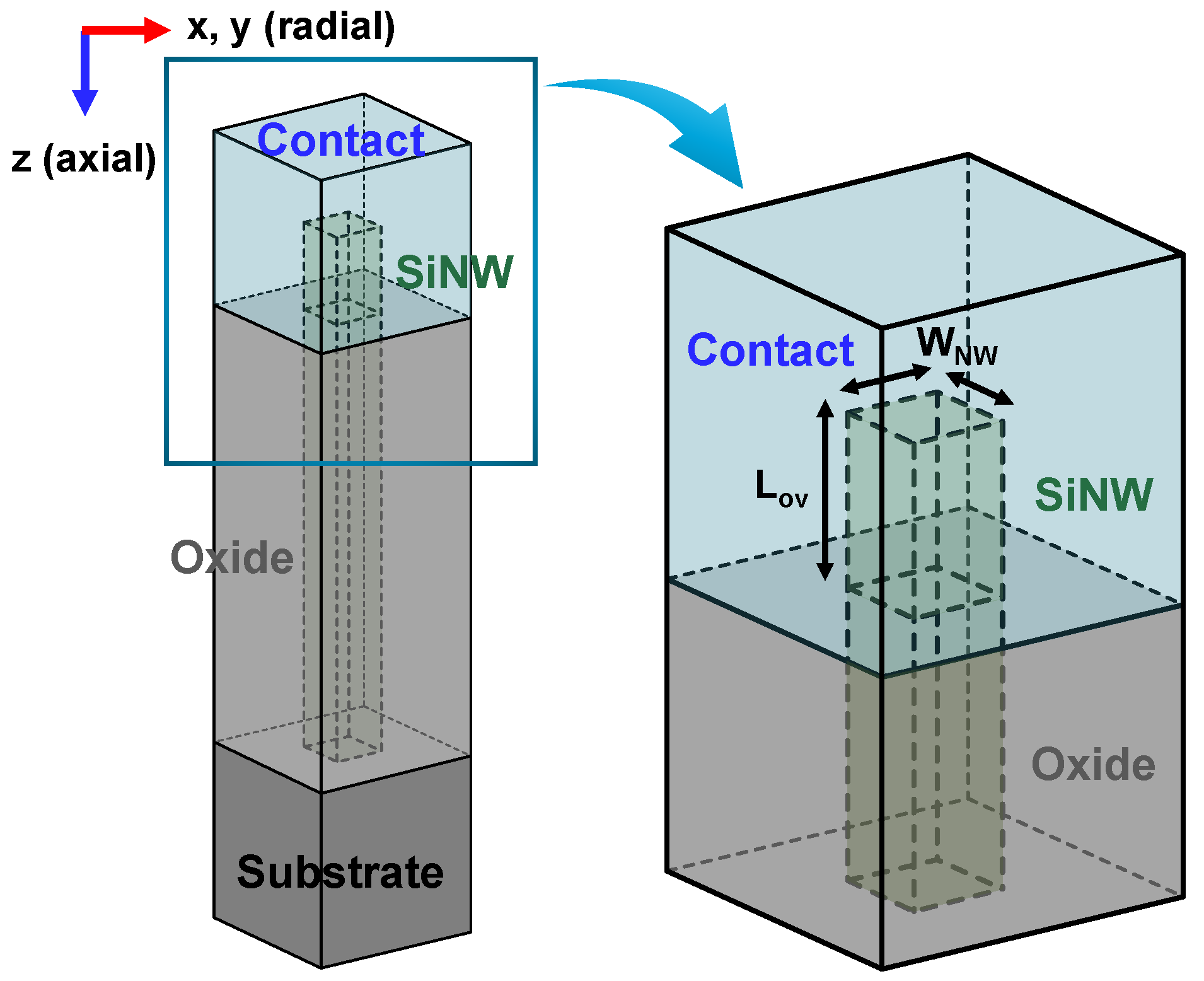
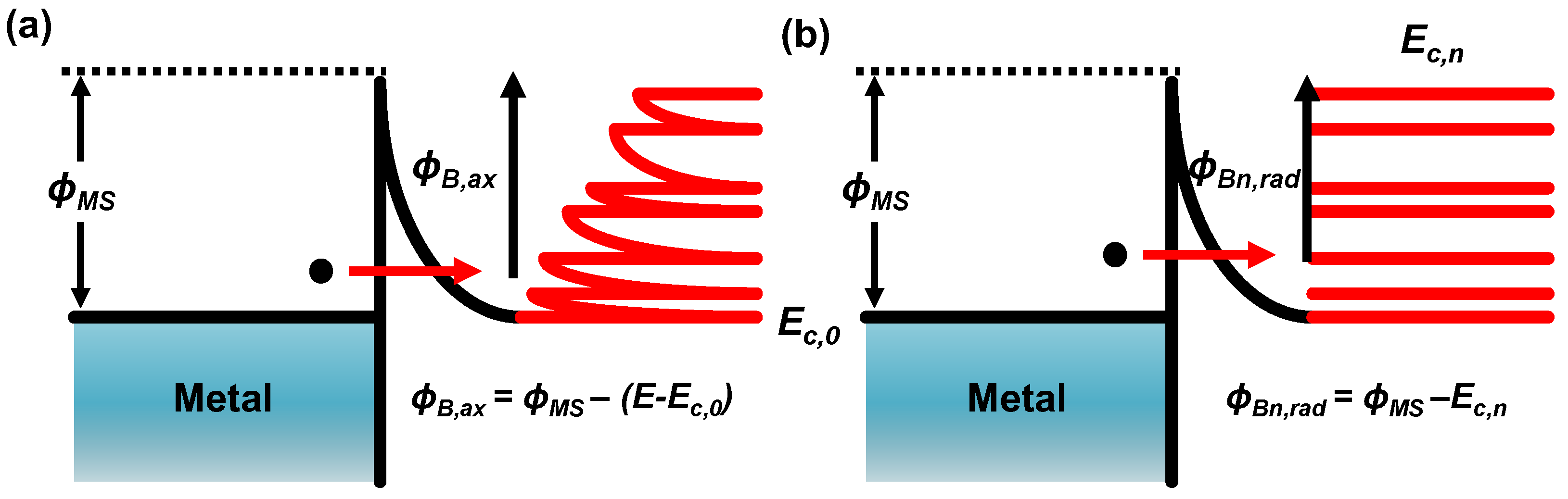
2. Modeling of Q1D Transport in Top Contact
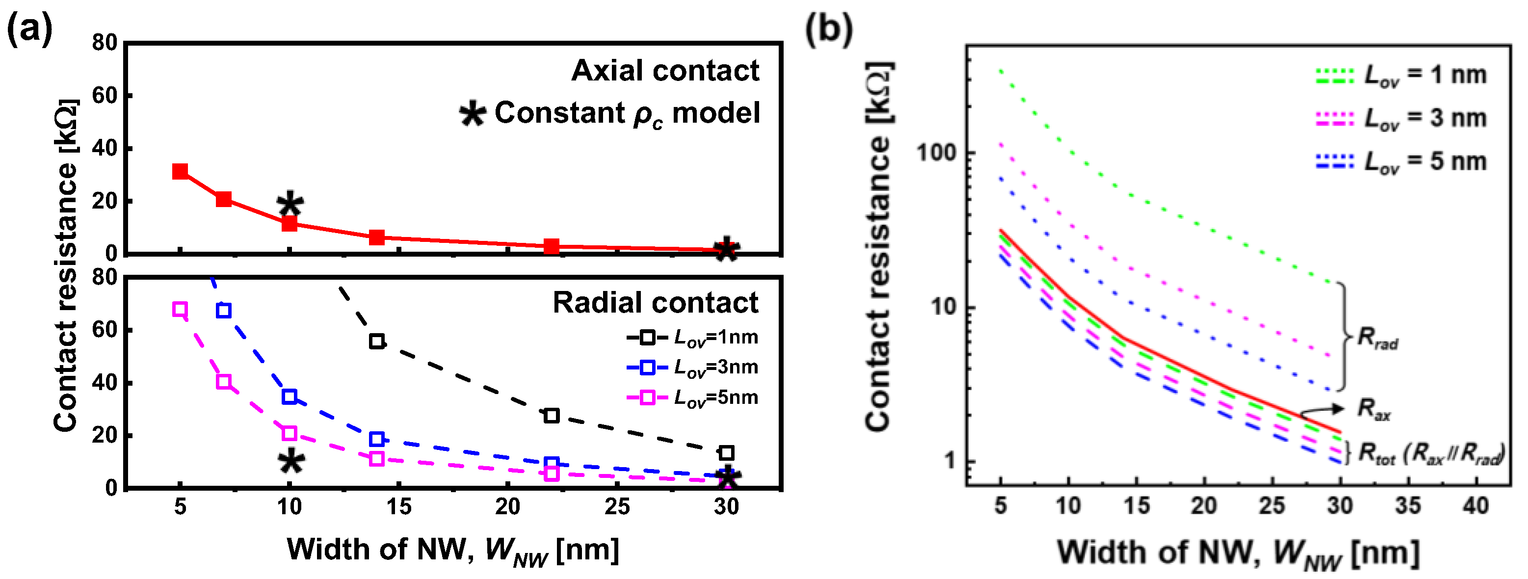
3. Calculation of Axial and Radial Contact Resistances
4. Conclusions
Author Contributions
Funding
Data Availability Statement
Conflicts of Interest
References
- Chidambaram, P.R.; Bowen, C.; Chakravarthi, S.; Machala, C.; Wise, R. Fundamentals of silicon material properties for successful exploitation of strain engineering in modern CMOS manufacturing. IEEE Trans. Electron Devices 2006, 53, 944–963. [Google Scholar] [CrossRef]
- Wu, C.C.; Lin, D.W.; Keshavarzi, A.; Huang, C.H.; Chan, C.T.; Tseng, C.H.; Chen, C.L.; Hsieh, C.Y.; Wong, K.Y.; Cheng, M.L.; et al. High performance 22/20nm FinFET CMOS devices with advanced high-k/metal gate scheme. In Proceedings of the 2010 IEEE International Electron Devices Meeting (IEDM), San Francisco, CA, USA, 6–8 December 2010. [Google Scholar]
- Tang, S.H.; Chang, L.; Lindert, N.; Choi, Y.-K.; Lee, W.-C.; Huang, X.; Subramanian, V.; Bokor, J.; King, T.-J.; Hu, C. FinFET-a quasiplanar double-gate MOSFET. In Proceedings of the 2001 IEEE International Solid-State Circuits Conference, San Francisco, CA, USA, 7 February 2001. [Google Scholar]
- Bangsaruntip, S.; Cohen, G.M.; Majumdar, A.; Zhang, Y.; Engelmann, S.U.; Fuller, N.C.M.; Gignac, L.M.; Mittal, S.; Newbury, J.S.; Guillorn, M.; et al. High performance and highly uniform gate-all-around silicon nanowire MOSFETs with wire size dependent scaling. In Proceedings of the 2009 IEEE International Electron Devices Meeting (IEDM), Baltimore, MD, USA, 7–9 December 2009. [Google Scholar]
- Lauer, I.; Loubet, N.; Kim, S.D.; Ott, J.A.; Mignot, S.; Venigalla, R.; Yamashita, T.; Standaert, T.; Faltermeier, J.; Basker, V.; et al. Si nanowire CMOS fabricated with minimal deviation from RMG FinFET technology showing record performance. In Proceedings of the 2015 Symposium on VLSI Technology, Kyoto, Japan, 16–18 June 2015. [Google Scholar]
- Mertens, H.; Ritzenthaler, R.; Chasin, A.; Schram, T.; Kunnen, E.; Hikavyy, A.; Ragnarsson, L.-Å.; Dekkers, H.; Hopf, T.; Wostyn, K.; et al. Vertically stacked gate-all-around Si nanowire CMOS transistors with dual work function metal gates. In Proceedings of the 2016 IEEE International Electron Devices Meeting (IEDM), San Francisco, CA, USA, 3–7 December 2016. [Google Scholar]
- Guerfi, Y.; Larrieu, G. Vertical silicon nanowire field effect transistors with nanoscale gate-all-around. Nanoscale Res. Lett. 2016, 11, 210. [Google Scholar] [CrossRef]
- Veloso, A.; Altamirano-Sánchez, E.; Brus, S.; Chan, B.T.; Cupak, M.; Dehan, M.; Delvaux, C.; Devriendt, K.; Eneman, G.; Ercken, M.; et al. Vertical nanowire FET integration and device aspects. ECS Trans. 2016, 72, 31–42. [Google Scholar] [CrossRef]
- Shafizade, D.; Shalcian, M.; Jazaeri, F. Ultrathin junctionless nanowire FET model, including 2-D quantum confinements. IEEE Trans. Electron Devices 2019, 66, 4101–4106. [Google Scholar] [CrossRef]
- Svensson, J.; Campbell, E. Schottky barriers in carbon nanotube-metal contacts. J. Appl. Phys. 2011, 110, 111101. [Google Scholar] [CrossRef]
- Wang, Z.-R.; Zhang, G.; Pey, K.-L.; Tung, C.H.; Lo, P.G.-Q. Schottky-Ohmic transition in metal-all-around electrical nanotubes to silicon nanowires. J. Appl. Phys. 2009, 105, 094508. [Google Scholar] [CrossRef]
- Léonard, F.; Talin, A.A. Size-dependent effects on electrical contacts to nanotubes and nanowires. Phys. Rev. Lett. 2006, 97, 026804. [Google Scholar] [CrossRef]
- Maheshwaram, S.; Manhas, S.K.; Kaushal, G.; Anand, B.; Singh, N. Vertical nanowire CMOS parasitic modeling and its performance analysis. IEEE Trans. Electron Devices 2013, 60, 2943–2950. [Google Scholar] [CrossRef]
- Ma, D.D.D.; Lee, C.S.; Au, F.C.K. Small-diameter silicon nanowire surfaces. Science 2003, 299, 1874–1877. [Google Scholar] [CrossRef] [PubMed]
- Yoffe, A.D. Low-dimensional systems: Quantum size effects and electronic properties of semiconductor microcrystallites (zero-dimensional systems) and some quasi-two-dimensional systems. Adv. Phys. 1993, 42, 173–262. [Google Scholar] [CrossRef]
- Léonard, F.; Tersoff, J. Role of Fermi-level pinning in nanotube Schottky diodes. Phys. Rev. Lett. 2000, 84, 4693. [Google Scholar] [CrossRef] [PubMed]

Disclaimer/Publisher’s Note: The statements, opinions and data contained in all publications are solely those of the individual author(s) and contributor(s) and not of MDPI and/or the editor(s). MDPI and/or the editor(s) disclaim responsibility for any injury to people or property resulting from any ideas, methods, instructions or products referred to in the content. |
© 2024 by the authors. Licensee MDPI, Basel, Switzerland. This article is an open access article distributed under the terms and conditions of the Creative Commons Attribution (CC BY) license (https://creativecommons.org/licenses/by/4.0/).
Share and Cite
Park, I.; Choi, J.; Kim, J.; Kong, B.D.; Lee, J.-S. Effect of Quasi-One-Dimensional Properties on Source/Drain Contacts in Vertical Nanowire Field-Effect Transistors (VNWFETs). Micromachines 2024, 15, 481. https://doi.org/10.3390/mi15040481
Park I, Choi J, Kim J, Kong BD, Lee J-S. Effect of Quasi-One-Dimensional Properties on Source/Drain Contacts in Vertical Nanowire Field-Effect Transistors (VNWFETs). Micromachines. 2024; 15(4):481. https://doi.org/10.3390/mi15040481
Chicago/Turabian StylePark, Iksoo, Jaeyong Choi, Jungsik Kim, Byoung Don Kong, and Jeong-Soo Lee. 2024. "Effect of Quasi-One-Dimensional Properties on Source/Drain Contacts in Vertical Nanowire Field-Effect Transistors (VNWFETs)" Micromachines 15, no. 4: 481. https://doi.org/10.3390/mi15040481
APA StylePark, I., Choi, J., Kim, J., Kong, B. D., & Lee, J.-S. (2024). Effect of Quasi-One-Dimensional Properties on Source/Drain Contacts in Vertical Nanowire Field-Effect Transistors (VNWFETs). Micromachines, 15(4), 481. https://doi.org/10.3390/mi15040481