


Radiation Detector Front-End Readout Chip with Nonbinary Successive Approximation Register Analog-to-Digital Converter for Wearable Healthcare Monitoring Applications

Abstract
1. Introduction
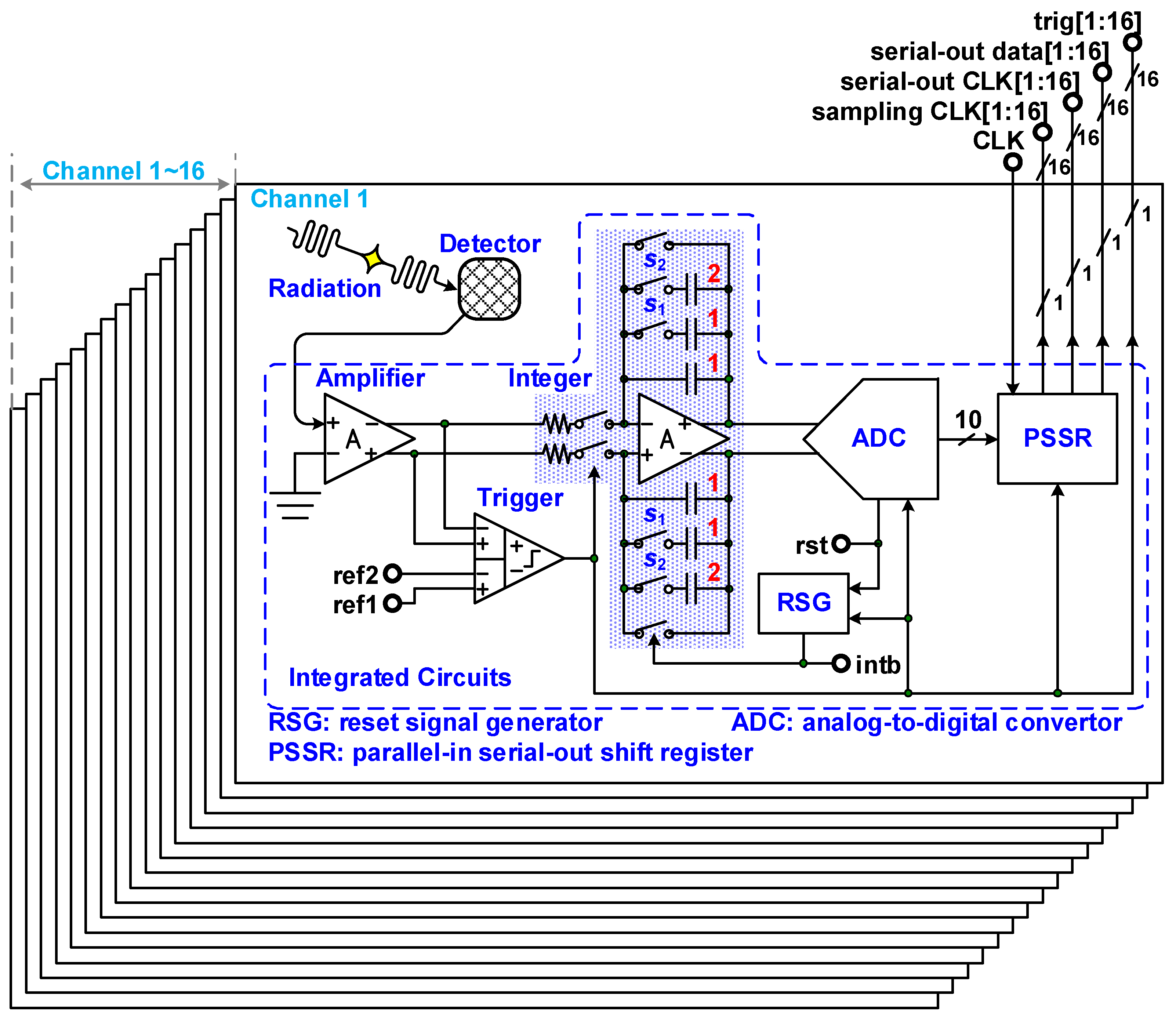
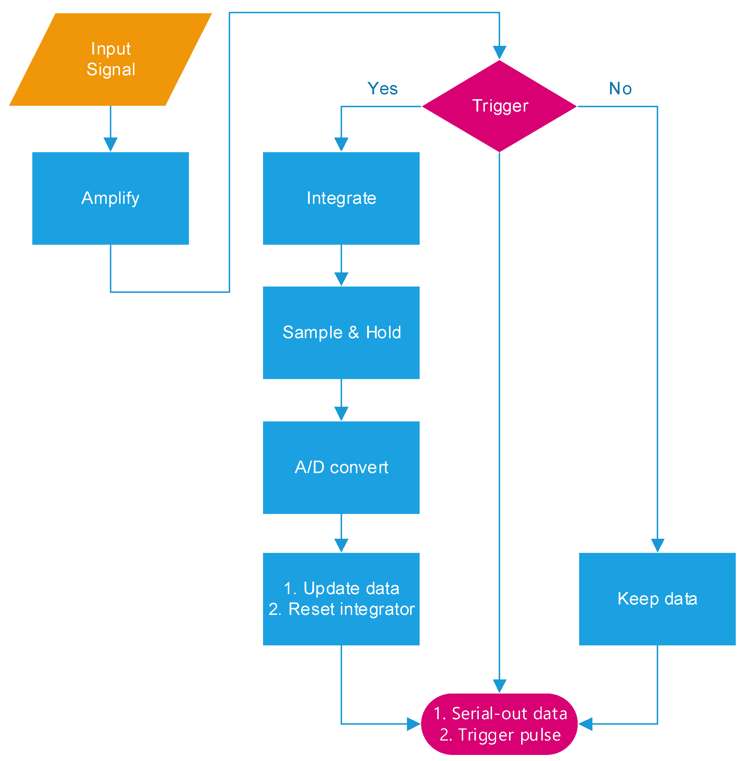
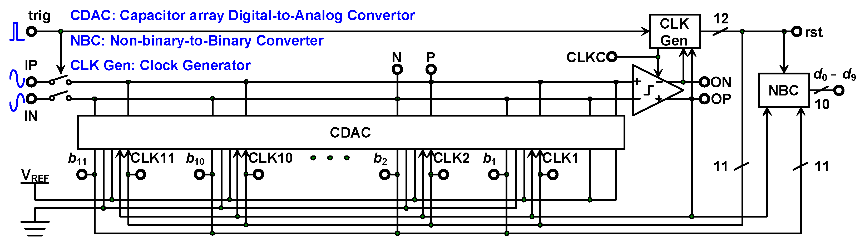
2. Proposed Structure
3. Circuit Design and Implementation
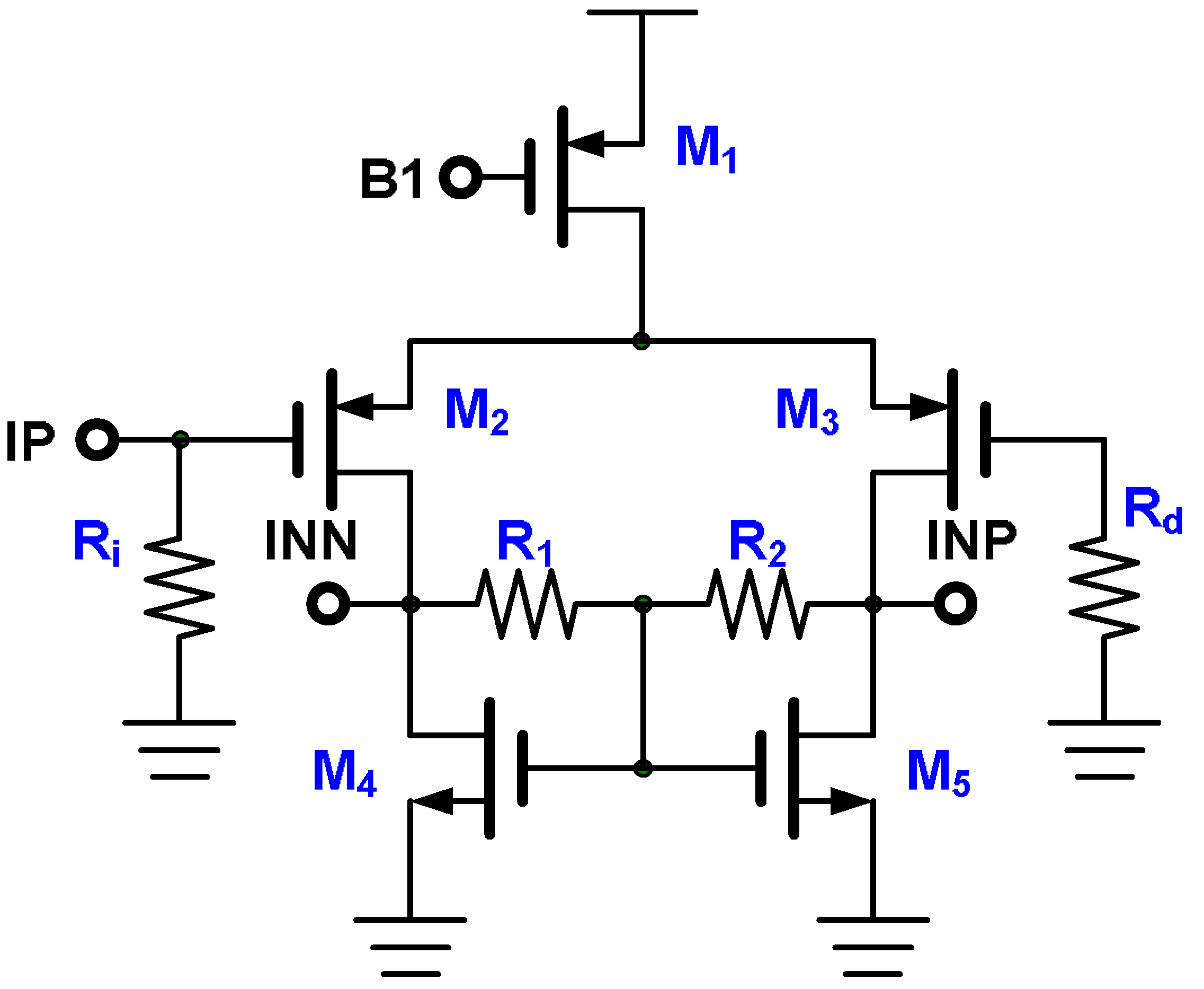
3.1. Amplifier
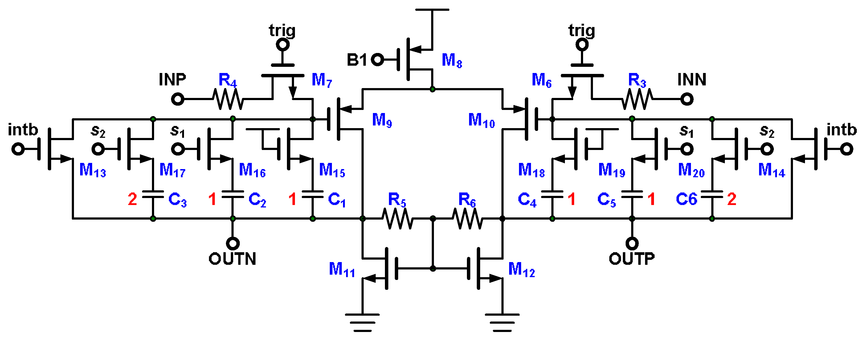
3.2. Integrator
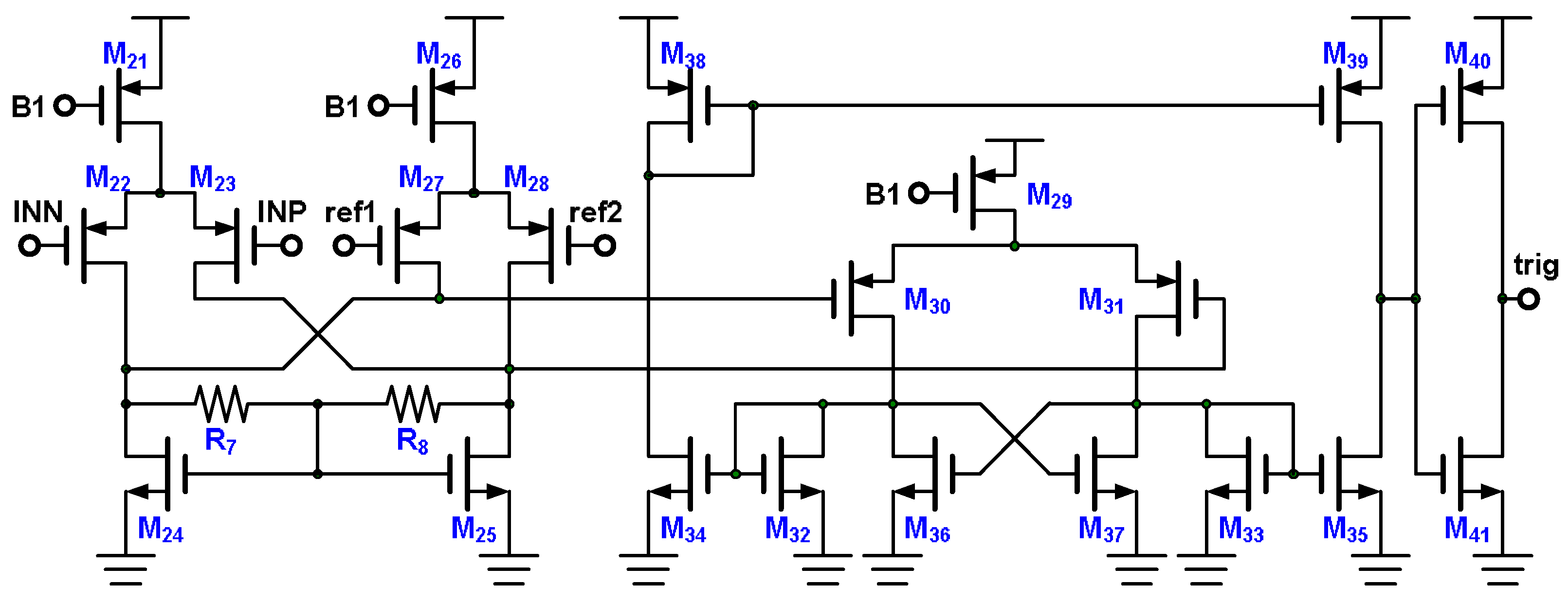
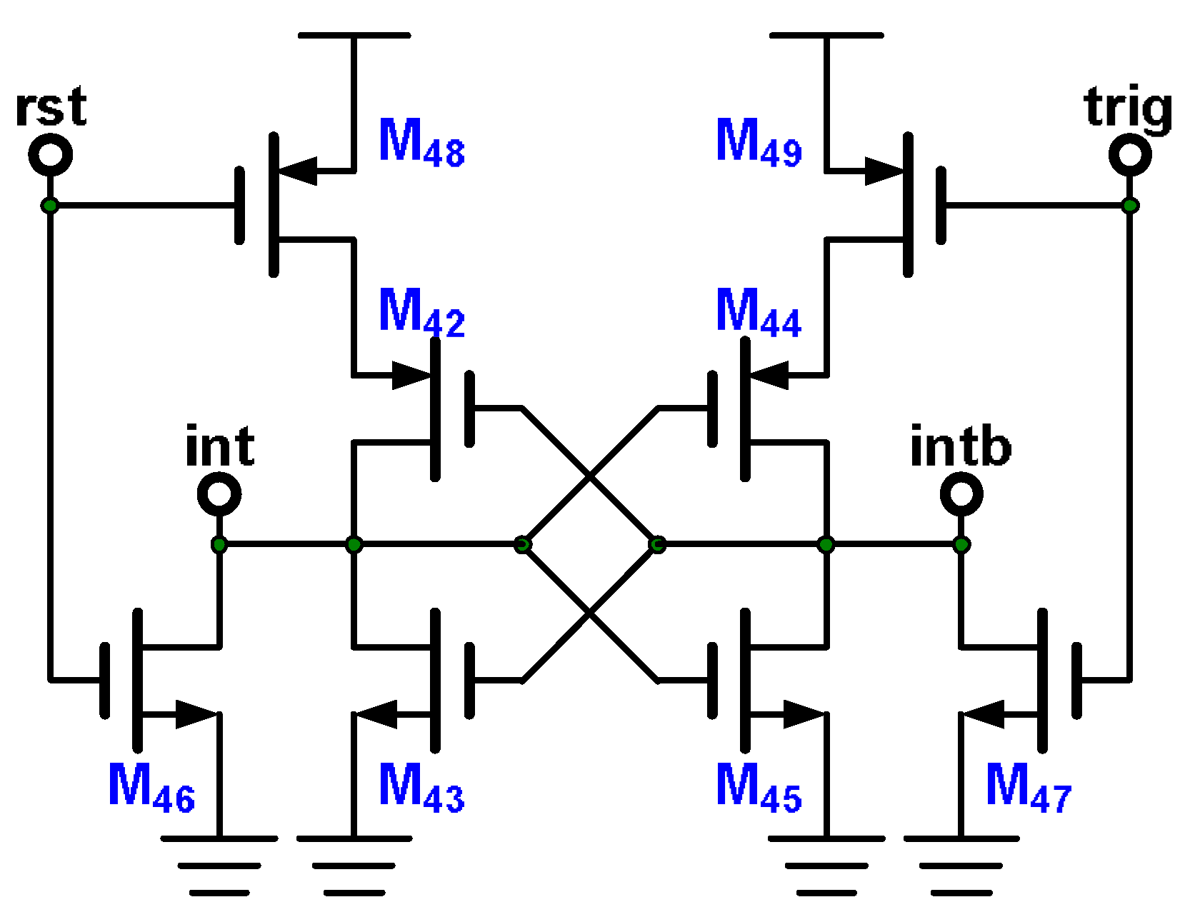
3.3. Trigger Generator
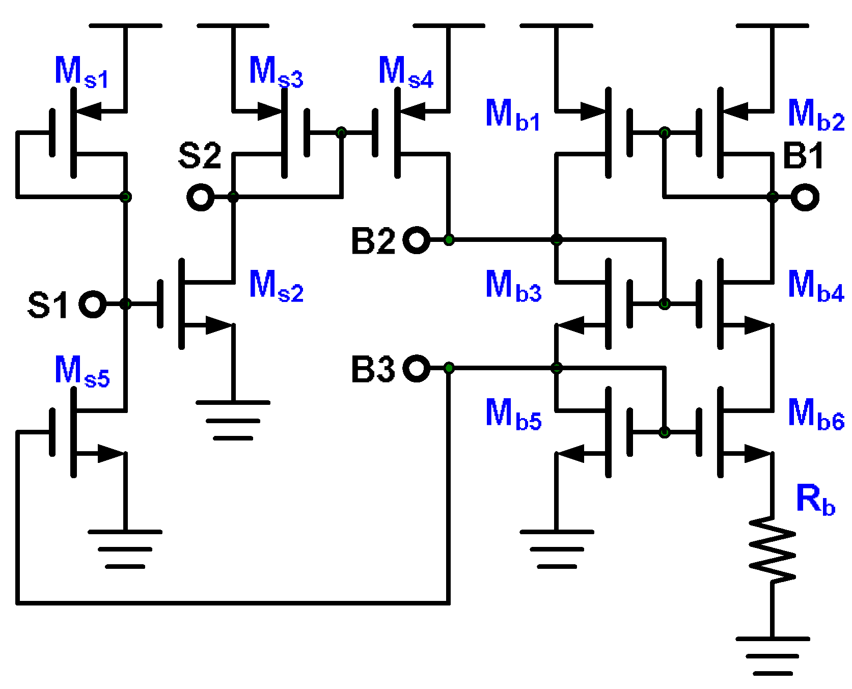
3.4. Bias Circuit
3.5. Reset Circuit
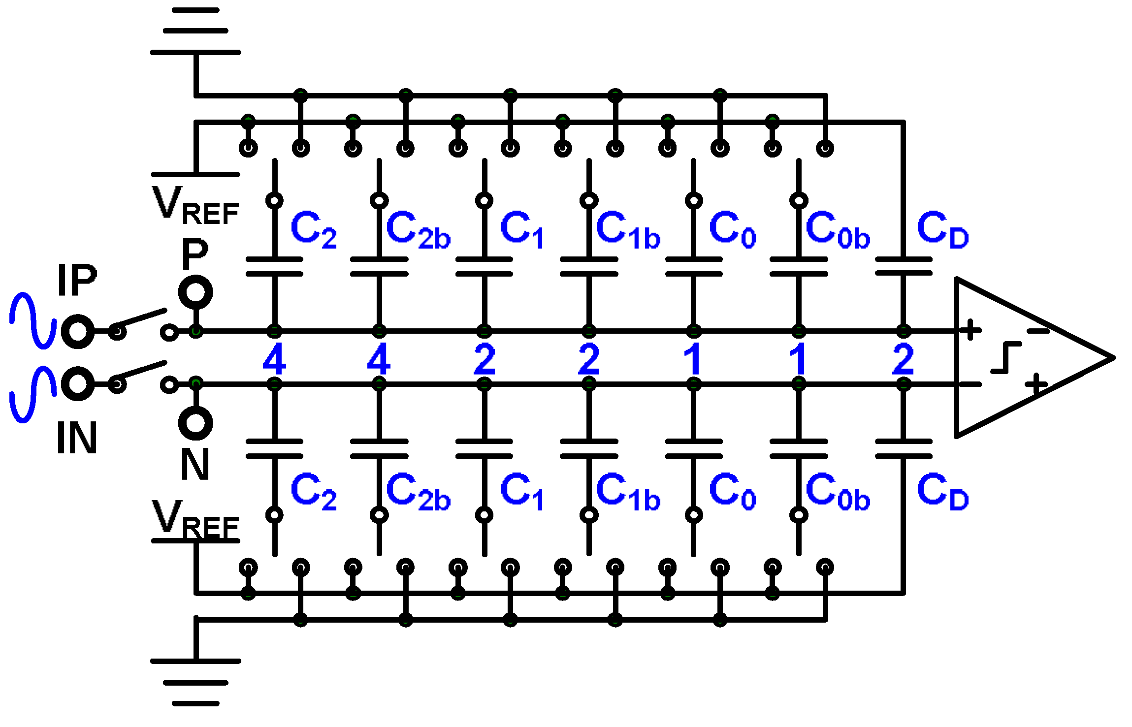
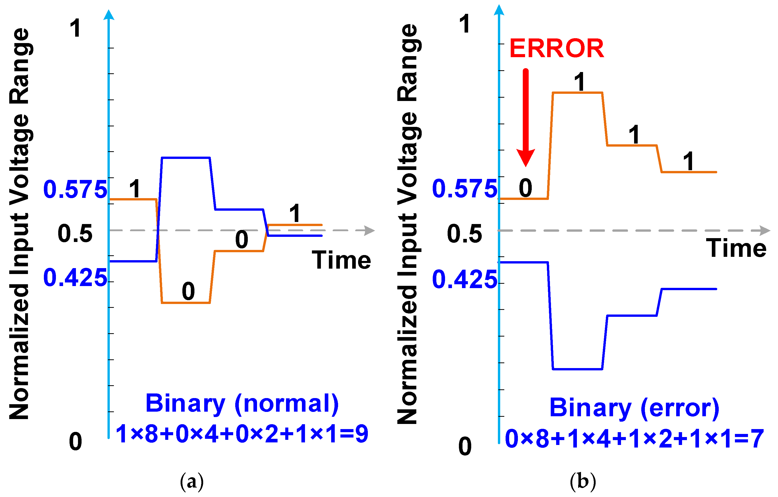
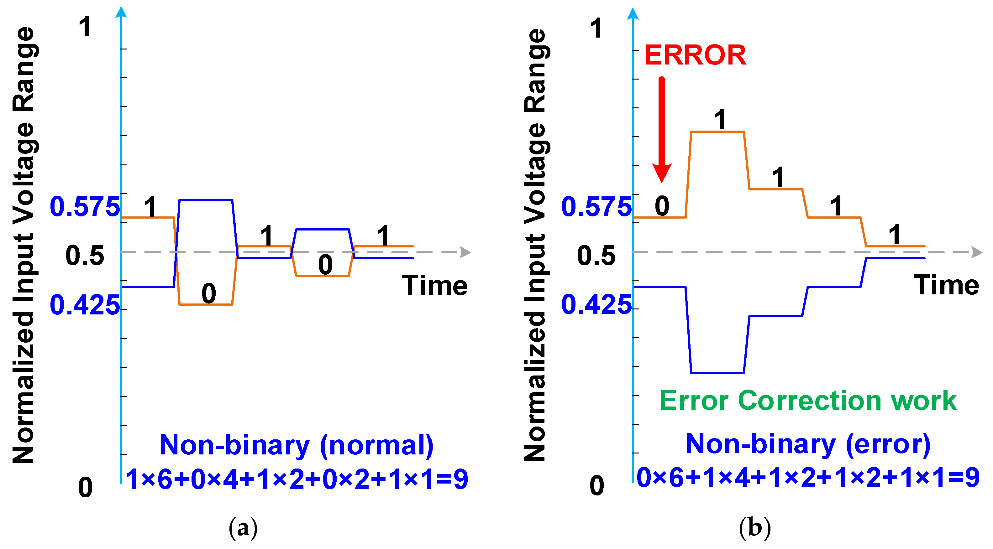
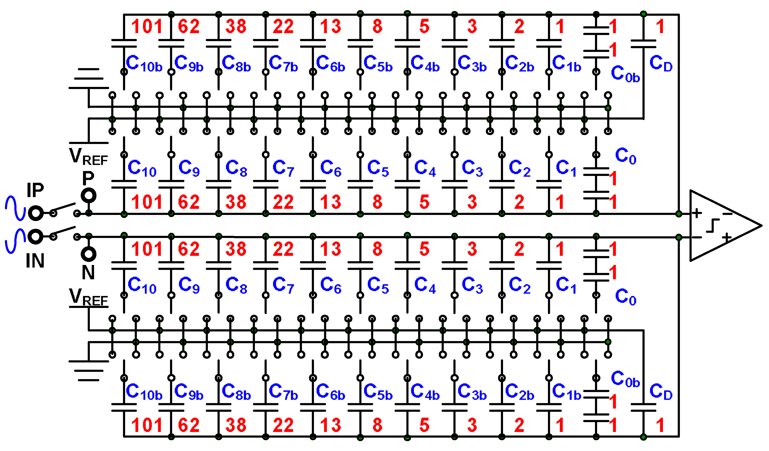
3.6. Nonbinary SAR ADC
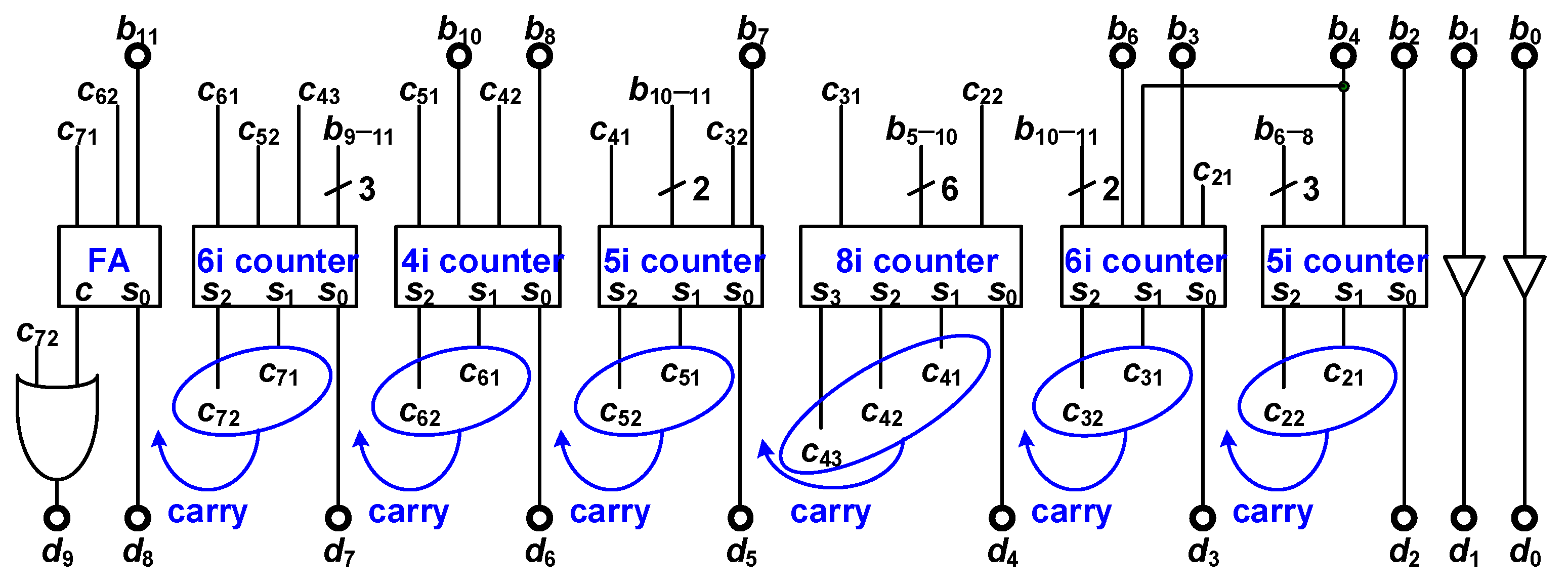
3.7. NBC
3.8. PSSR
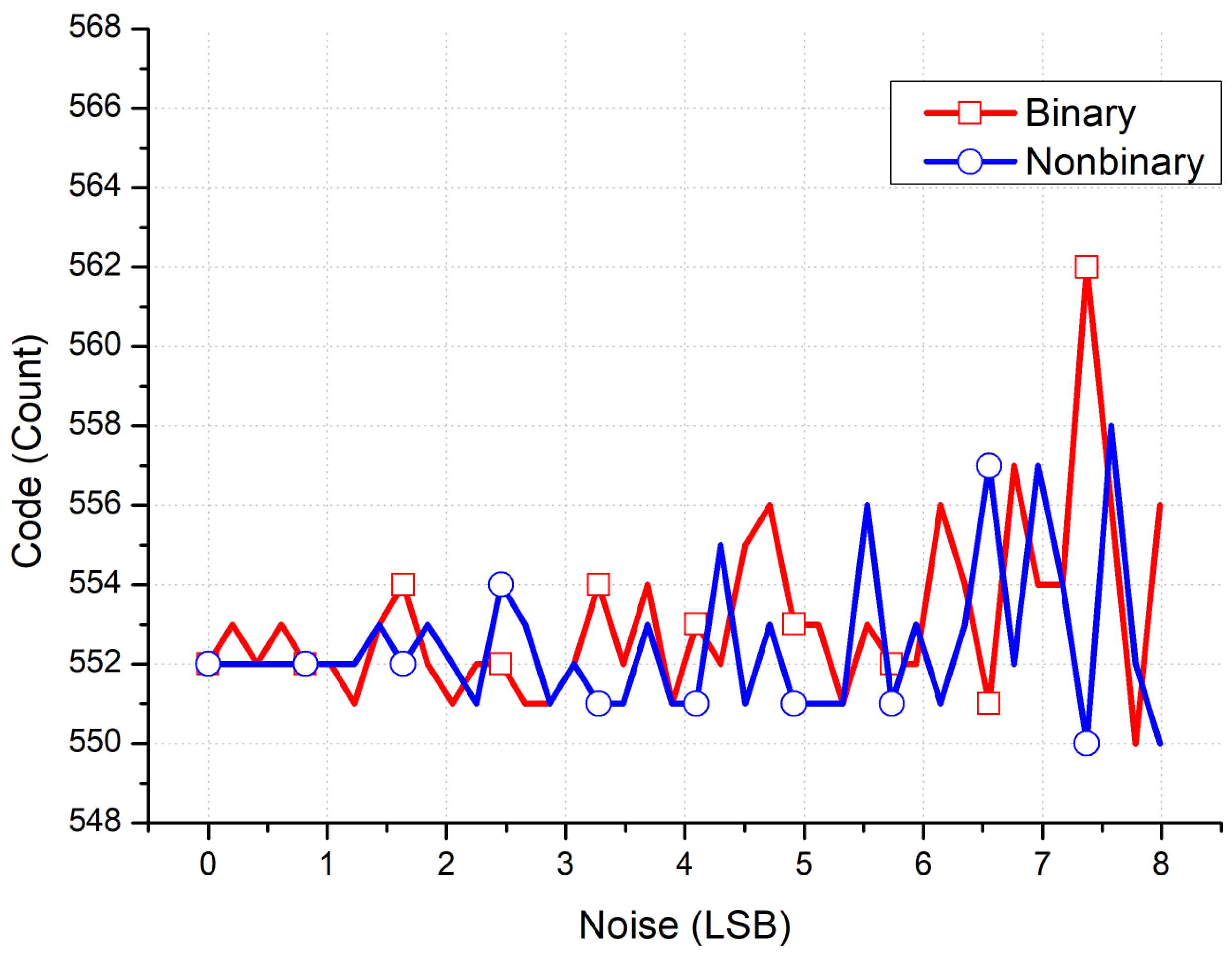
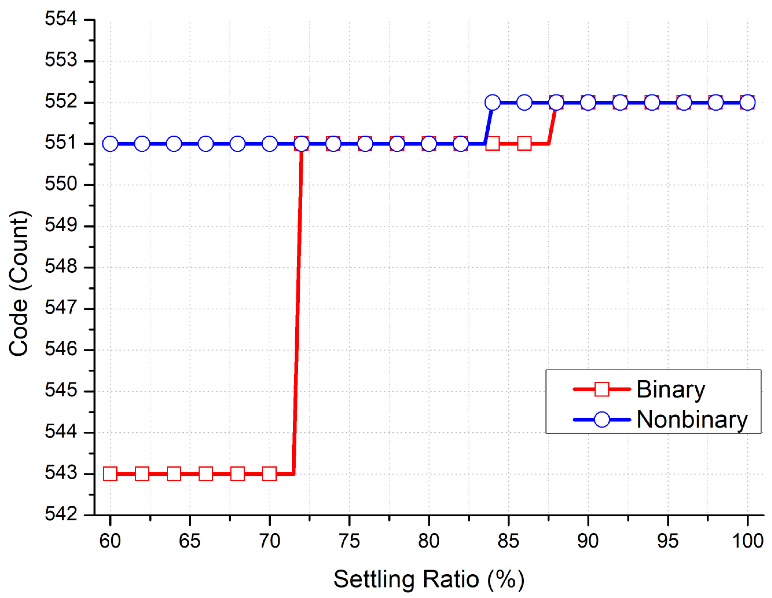
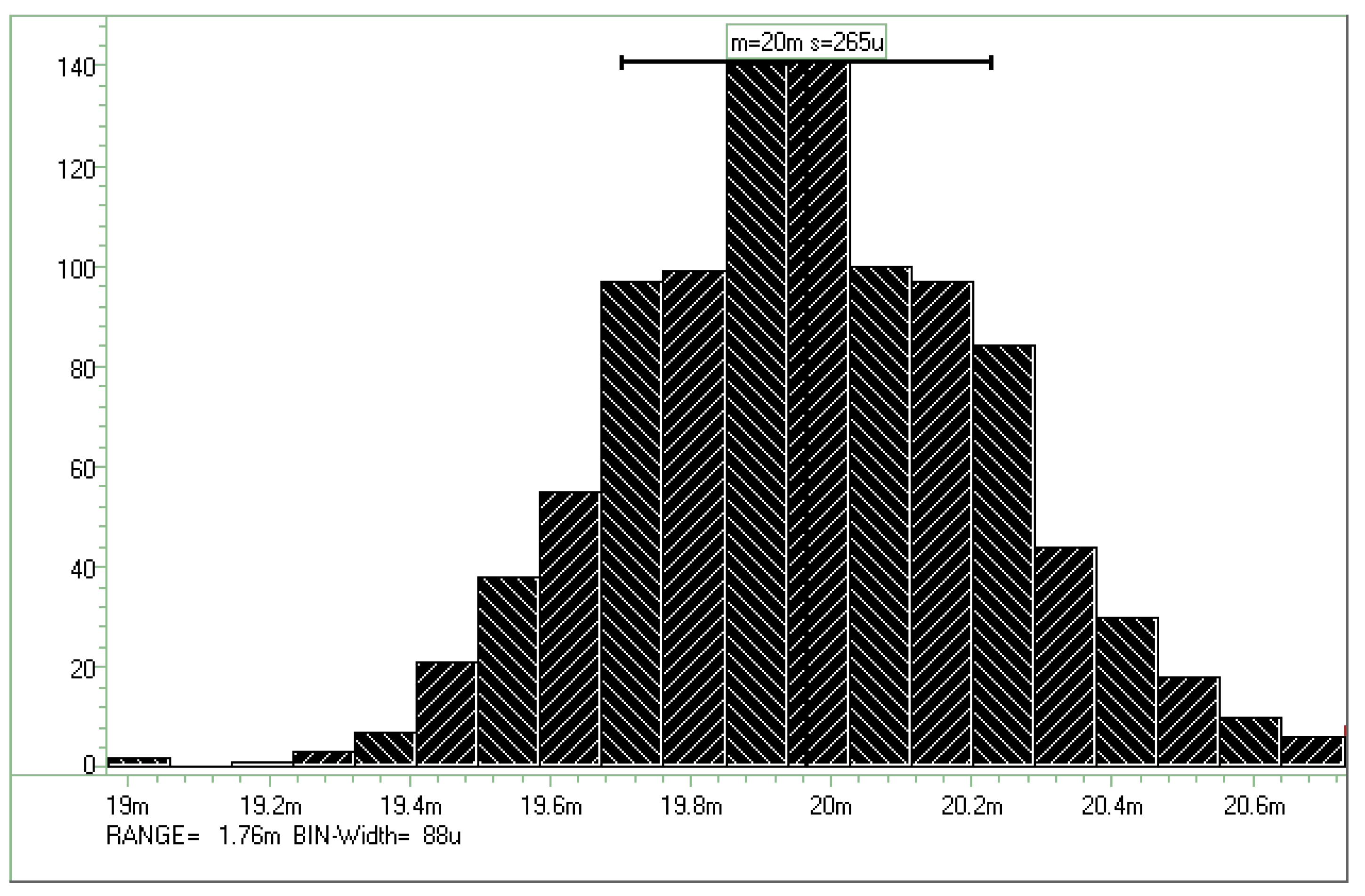
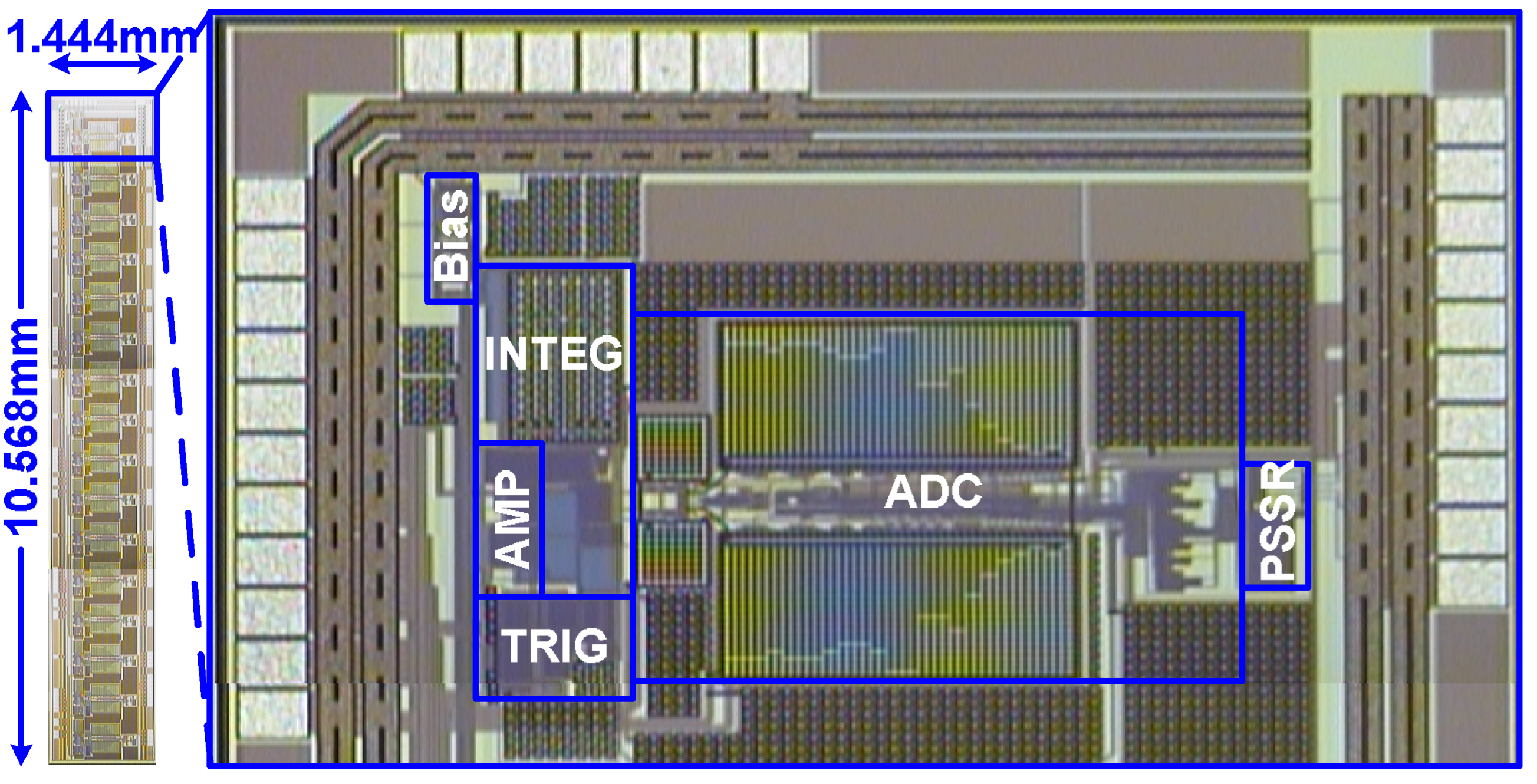
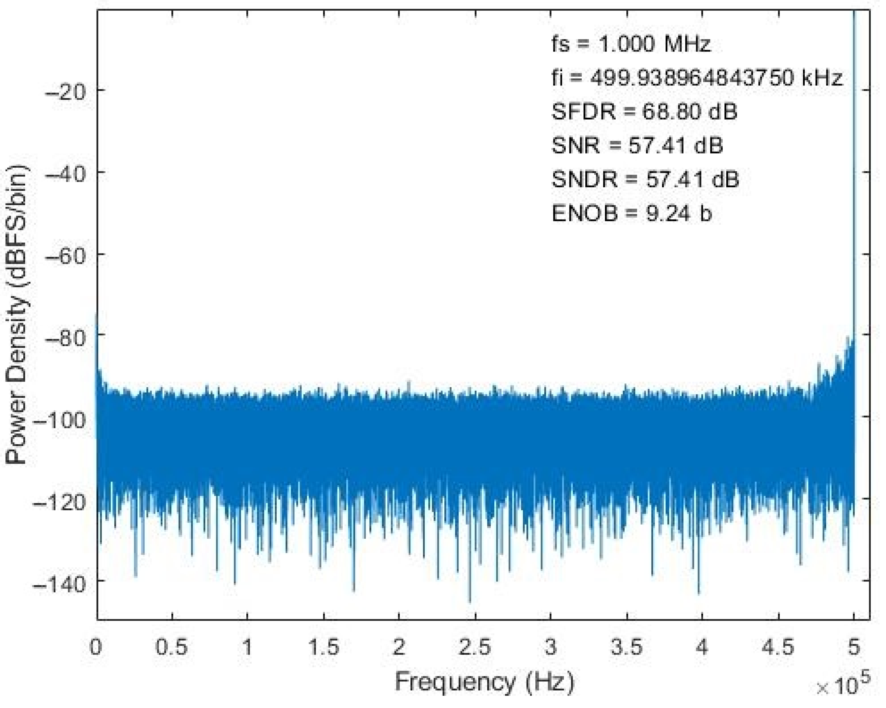
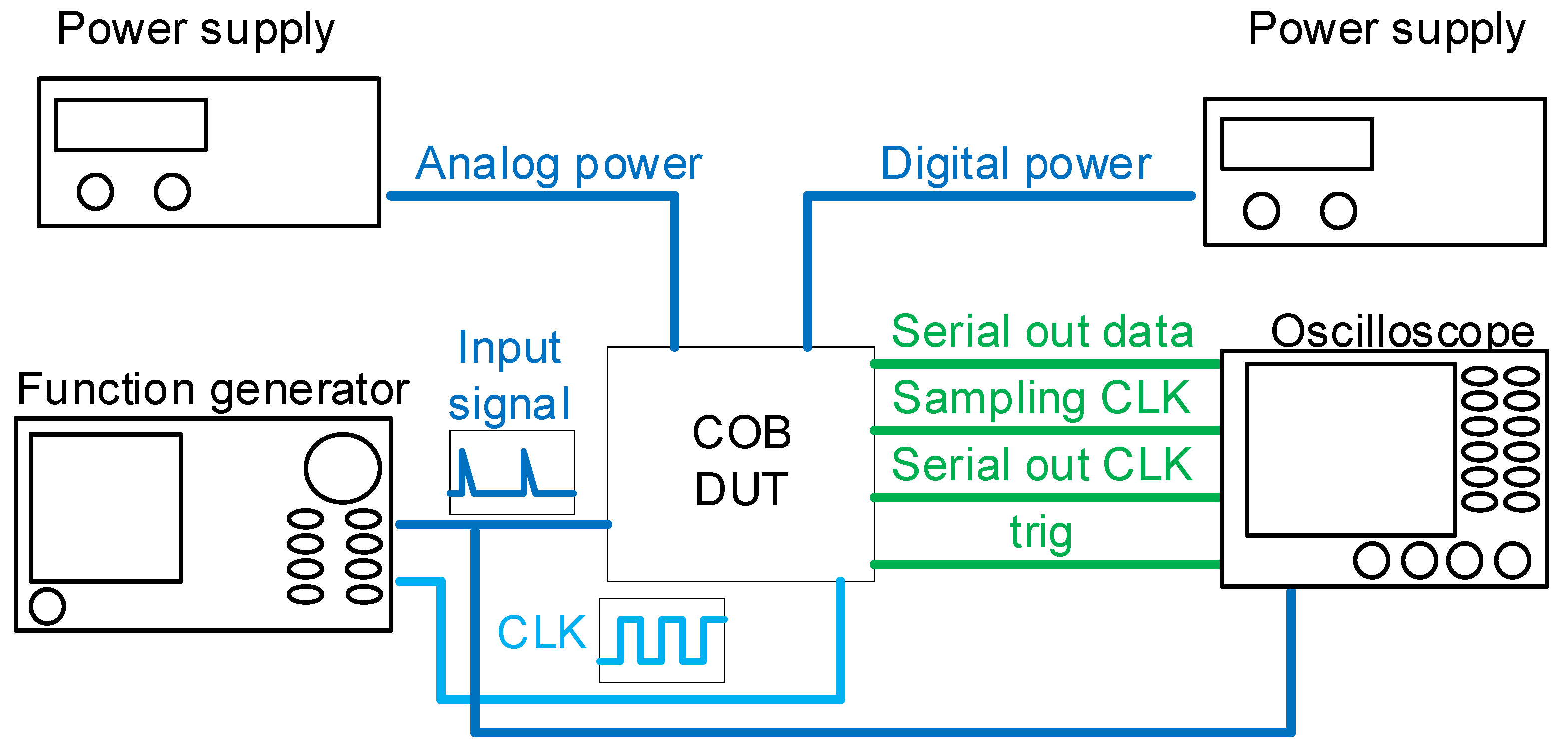
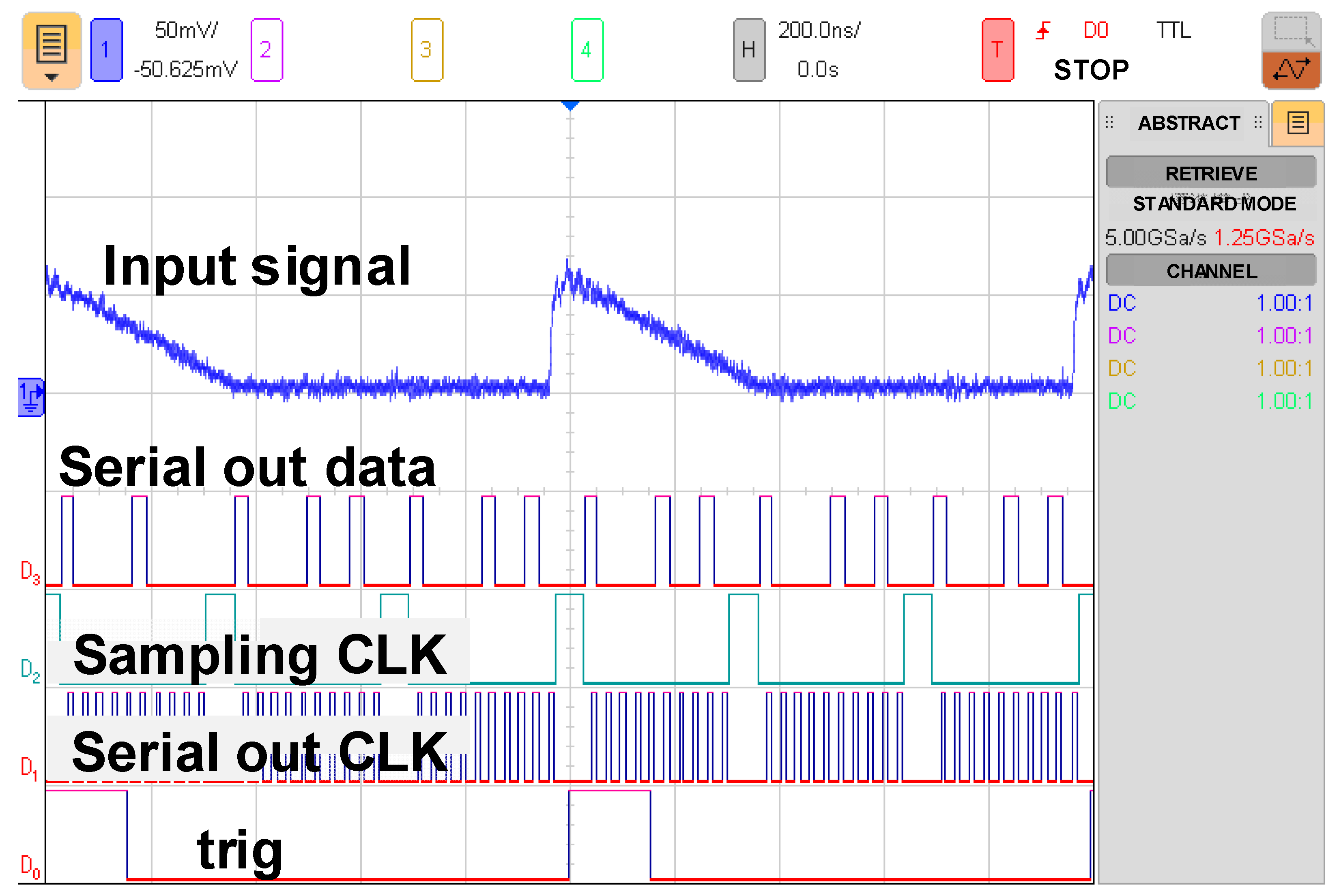
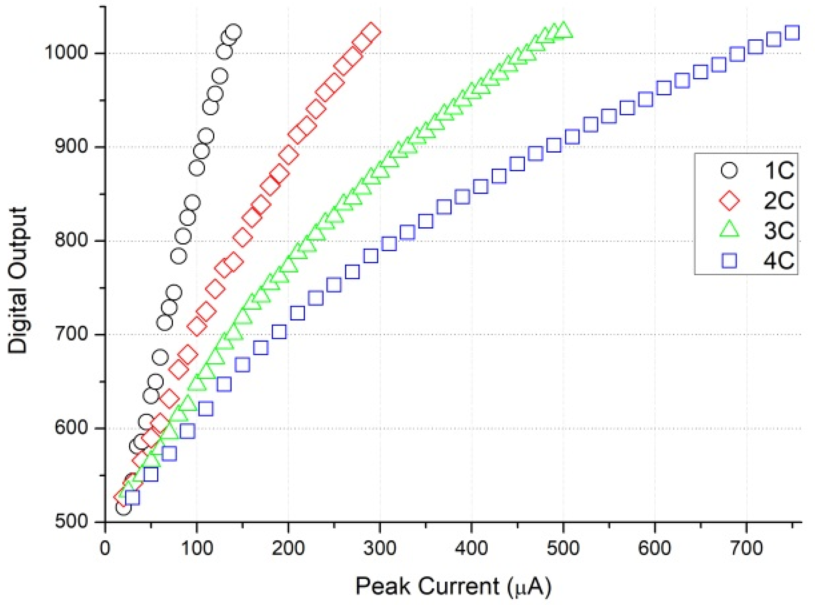
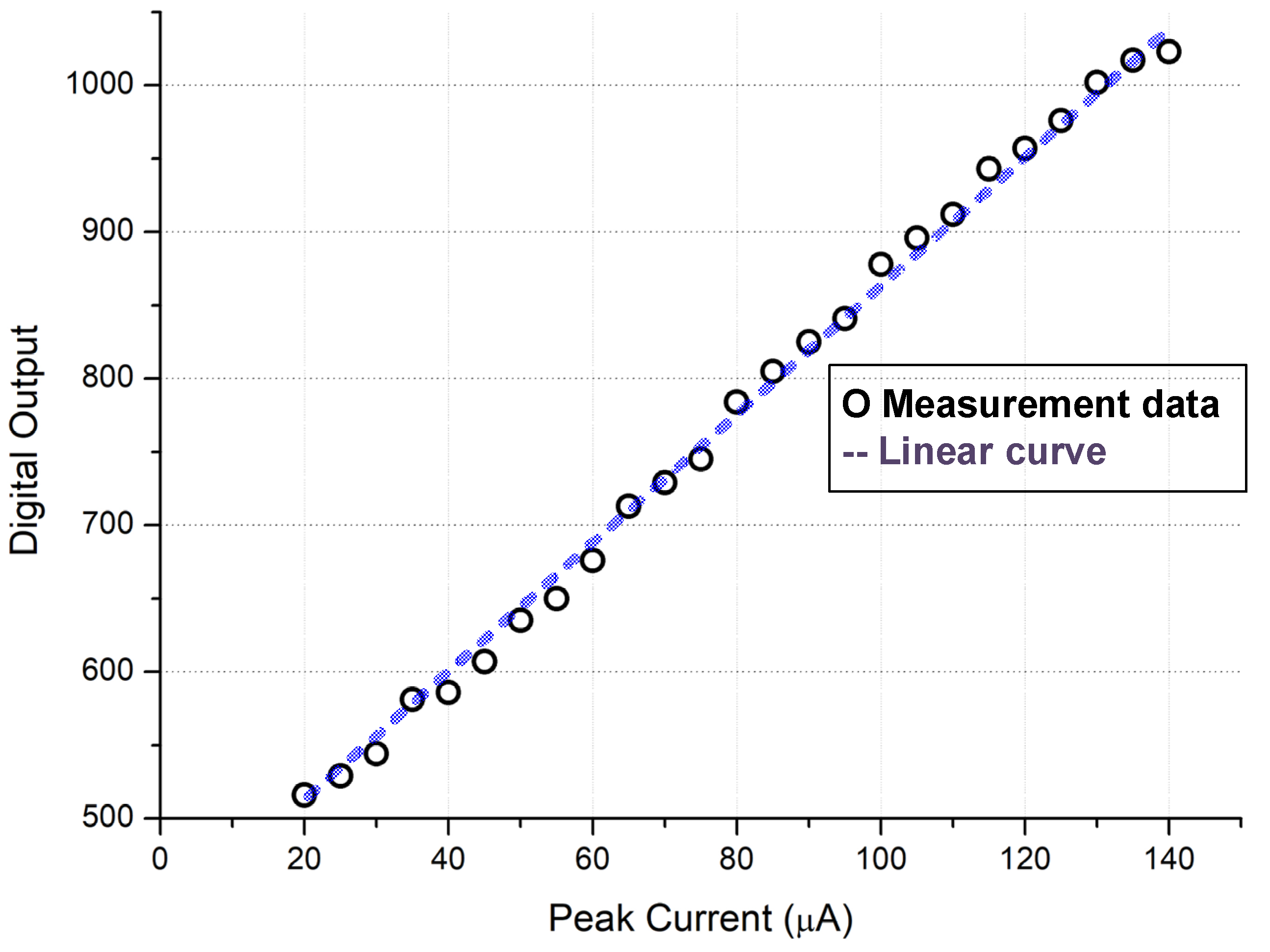
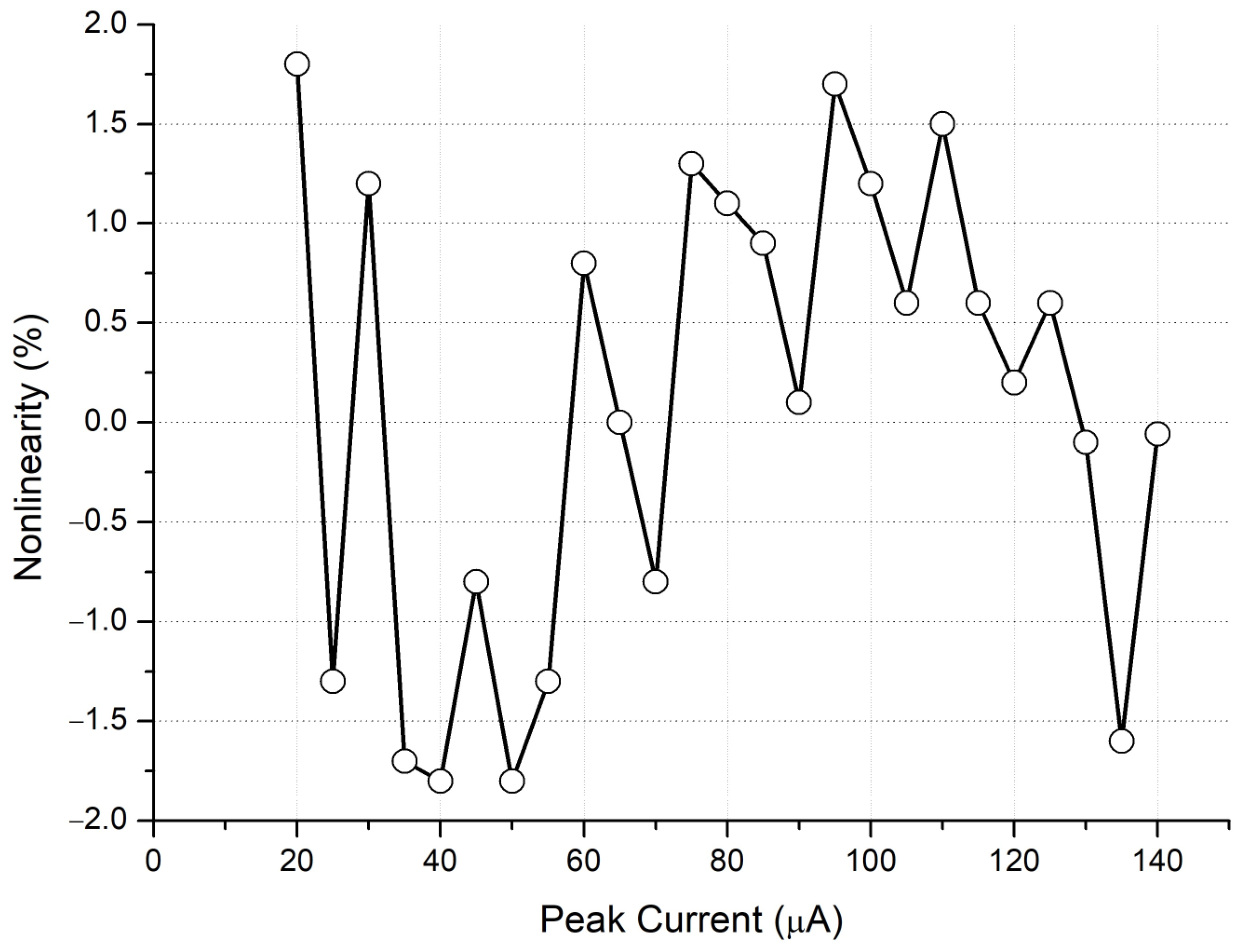
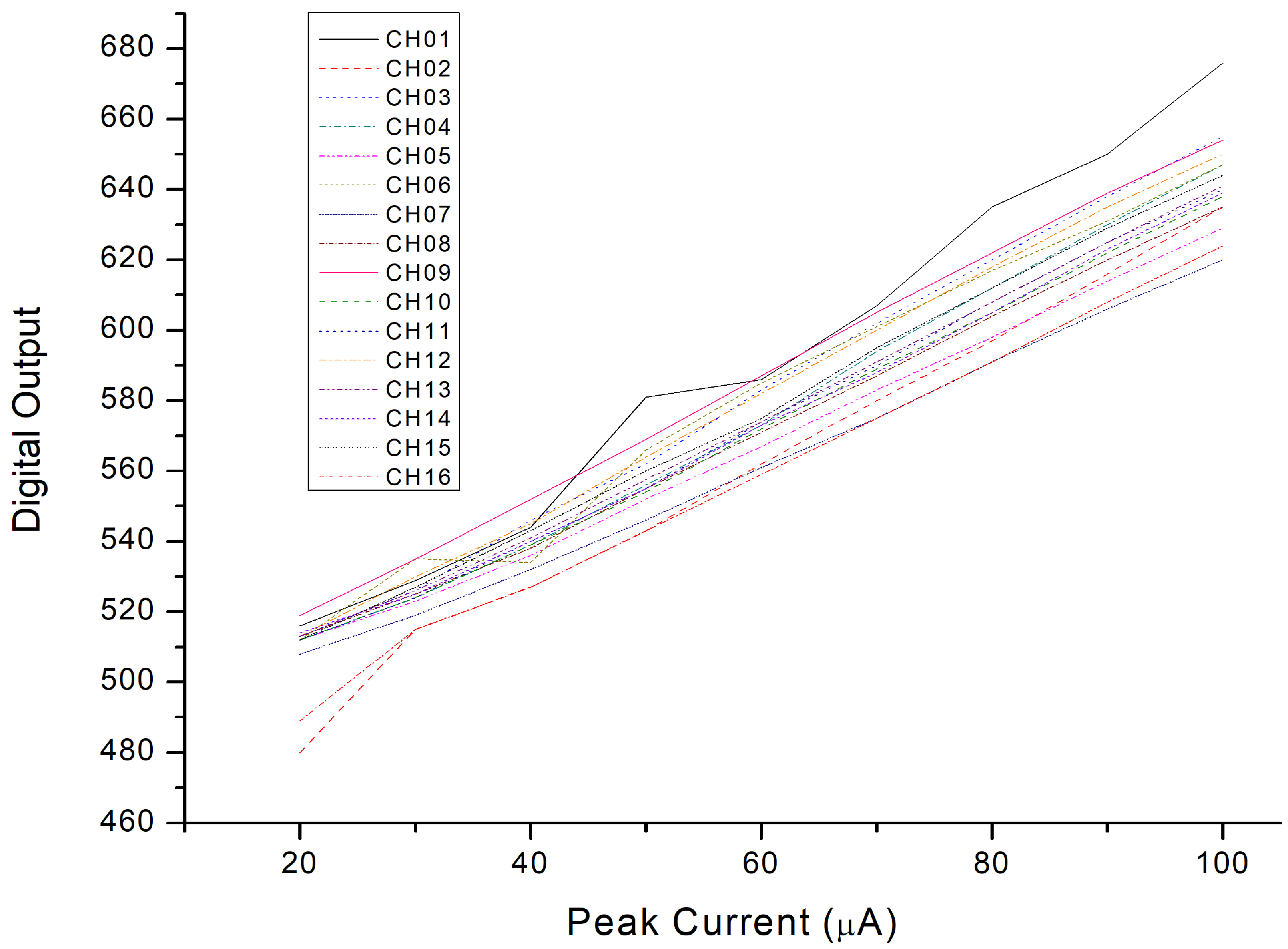
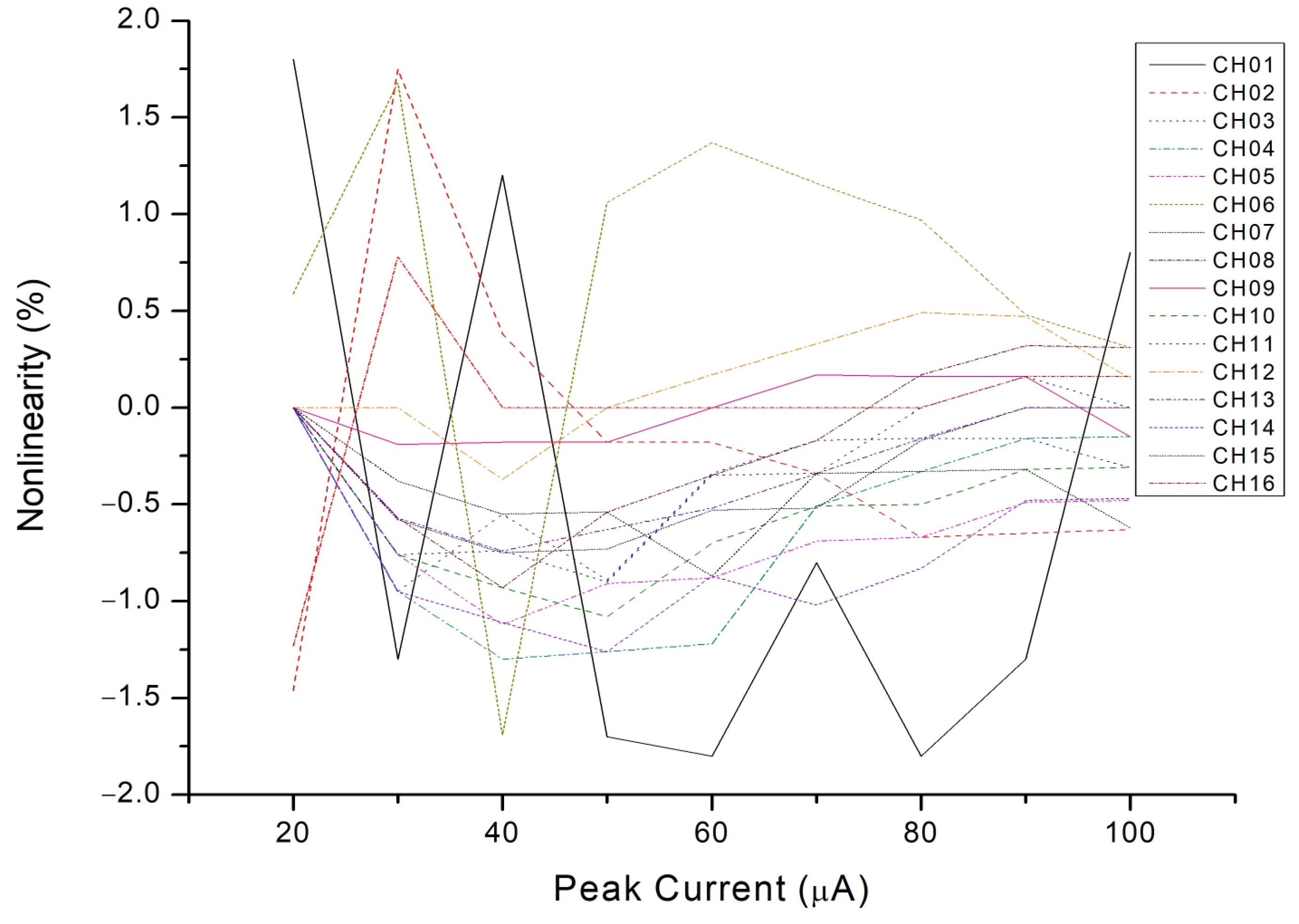
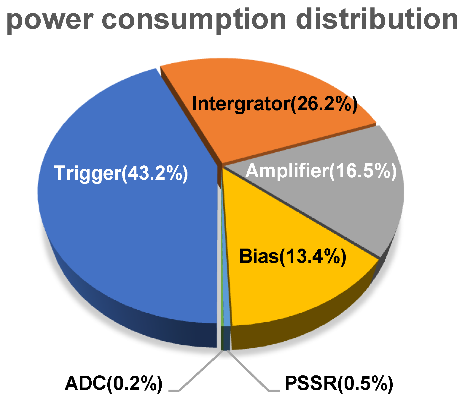
4. Measurement Results
5. Conclusions
Author Contributions
Funding
Data Availability Statement
Acknowledgments
Conflicts of Interest
References
- Hsu, W.-Y.; Cheng, Y.-W. EEG-Channel-Temporal-Spectral-Attention Correlation for Motor Imagery EEG Classification. IEEE Trans. Neural Syst. Rehabil. Eng. 2023, 31, 1659–1669. [Google Scholar] [CrossRef] [PubMed]
- Ozkan, H.; Ozhan, O.; Karadana, Y.; Gulcu, M.; Macit, S.; Husain, F. A Portable Wearable Tele-ECG Monitoring System. IEEE Trans. Instrum. Meas. 2020, 69, 173–182. [Google Scholar] [CrossRef]
- Teferra, M.N.; Hobbs, D.A.; Clark, R.A.; Reynolds, K.J. Electronic-Textile 12-Lead Equivalent Diagnostic Electrocardiogram Based on the EASI Lead Placement. IEEE Sens. J. 2022, 22, 5994–6001. [Google Scholar] [CrossRef]
- Quiroz-Juárez, M.A.; Jiménez-Ramírez, O.; Vázquez-Medina, R.; Ryzhii, E.; Ryzhii, M.; Aragón, J.L. Cardiac Conduction Model for Generating 12 Lead ECG Signals With Realistic Heart Rate Dynamics. IEEE Trans. Nanobiosci. 2018, 17, 525–532. [Google Scholar] [CrossRef] [PubMed]
- Yang, W.; Wang, S. A Privacy-Preserving ECG-Based Authentication System for Securing Wireless Body Sensor Networks. IEEE Internet Things J. 2022, 9, 6148–6158. [Google Scholar] [CrossRef]
- Bortolotti, D.; Mangia, M.; Bartolini, A.; Rovatti, R.; Setti, G.; Benini, L. Energy-Aware Bio-Signal Compressed Sensing Reconstruction on the WBSN-Gateway. IEEE Trans. Emerg. Top. Comput. 2018, 6, 370–381. [Google Scholar] [CrossRef]
- Morahan, A.J.; D’Adda, I.; Erlandsson, K.; Carminati, M.; Rega, M.; Walls, D.; Fiorini, C.; Hutton, B.F. Challenges in Acquiring Clinical Simultaneous SPECT-MRI on a PET-MRI Scanner. IEEE Trans. Radiat. Plasma Med. Sci. 2023, 7, 755–763. [Google Scholar] [CrossRef]
- Zhang, Z.; Yu, Q.; Zhang, Q.; Li, J.; Wu, K.; Ning, N. A Code-Recombination Algorithm-Based ADC With Feature Extraction for WBSN Applications. IEEE Trans. Very Large Scale Integr. (VLSI) Syst. 2022, 30, 134–142. [Google Scholar] [CrossRef]
- Surti, S.; Werner, M.E.; Perkins, A.E.; Kolthammer, J.; Karp, J.S. Performance of Philips Gemini TF PET/CT scanner with special consideration for its time-of-flight imaging capabilities. J. Nucl. Med. 2007, 48, 471–480. [Google Scholar]
- Muzic, R.F.; Kolthammer, J.A. PET performance of the Gemini TF: A time-of-flight PET/CT scanner. Proc. IEEE Nucl. Sci. Symp. Conf. Rec. 2006, 3, 1940–1944. [Google Scholar] [CrossRef]
- Ollivier-Henry, N.; Gao, W.; Mbow, N.A.; Brasse, D.; Humbert, B.; HuGuo, C.; Colledani, C.; Hu, Y. Design and Characteristics of a Full-Custom Multichannel Front-End Readout ASIC Using Current-Mode CSA for Small Animal PET Imaging. IEEE Trans. Biomed. Circuits Syst. 2011, 5, 90–99. [Google Scholar] [CrossRef] [PubMed]
- Gao, W.; Gao, D.; Wei, T.; Zeng, H.; Duan, Y.; Lu, S.; Shen, L.; Xu, W.; Xie, Q.; Hu, Y. Design of a Monolithic Multi-Channel Front-End Readout ASIC for LYSO/SiPM-based SmallAnimal Flat-Panel PET Imaging. In Proceedings of the 2011 IEEE Nuclear Science Symposium Conference Record, Valencia, Spain, 23–29 October 2011; pp. 2447–2450. [Google Scholar] [CrossRef]
- Schemm, N.; Balkır, S.; Hoffman, M.W. A 4-μW CMOS Front End for Particle Detection Applications. IEEE Trans. Circuits Syst.—II Express Briefs 2010, 57, 100–104. [Google Scholar] [CrossRef]
- Gao, W.; Gao, D.; Hu-Guo, C.; Wei, T.; Hu, Y. Design and Characteristics of an Integrated Multichannel Ramp ADC Using Digital DLL Techniques for Small Animal PET Imaging. IEEE Trans. Nucl. Sci. 2011, 58, 2161–2168. [Google Scholar] [CrossRef]
- Braga, L.H.C.; Gasparini, L.; Grant, L.; Henderson, R.K.; Massari, N.; Perenzoni, M.; Stoppa, D.; Walker, R. A Fully Digital 8 × 16 SiPM Array for PET Applications with Per-Pixel TDCs and Real-Time Energy Output. IEEE J. Solid-State Circuits 2014, 49, 301–314. [Google Scholar] [CrossRef]
- Kuttner, F. A 1.2V 10b 20MSample/s Non-Binary Successive Approximation ADC in 0.13μm CMOS. In Proceedings of the 2002 IEEE International Solid-State Circuits Conference, Digest of Technical Papers (Cat. No.02CH37315), San Francisco, CA, USA, 7 February 2002; pp. 176–177. [Google Scholar] [CrossRef]
- Qiu, L.; Wang, K.; Yang, C.; Zheng, Y. A Low Power Pre-Setting Based Sub-Radix-2 Approximation for Multi-bit/cycle SAR ADCs. IEEE Access 2020, 8, 83062–83069. [Google Scholar] [CrossRef]
- Ginsburg, B.P.; Chandrakasan, A.P. 500-MS/s 5-bit ADC in 65-nm CMOS with Split Capacitor Array DAC. IEEE J. Solid-State Circuits 2007, 42, 739–747. [Google Scholar] [CrossRef]
- Zhang, Q.; Ning, N.; Li, J.; Yu, Q.; Zhang, Z.; Wu, K. A High Area-Efficiency 14-bit SAR ADC with Hybrid Capacitor DAC for Array Sensors. IEEE Trans. Circuits Syst. I Regul. Pap. 2020, 67, 4396–4408. [Google Scholar] [CrossRef]
- Razavi, B. Design of Analog CMOS Integrated Circuit; McGraw-Hill: Boston, UK, 2006; pp. 209, 378–381, 465. [Google Scholar]
- Mahmoud, S.A.; Soliman, A.M. Soliman. The Differential Difference Operational Floating Amplifier: A New Block for Analog Signal Processing in MOS Technology. IEEE Trans. Circuits Syst. II Analog Digit. Signal Process. 1998, 45, 148–158. [Google Scholar] [CrossRef]
- Verma, N.; Chandrakasan, A.P. An Ultra Low Energy 12-bit Rate-Resolution Scalable SAR ADC for Wireless Sensor Nodes. IEEE J. Solid-State Circuits 2007, 42, 1196–1205. [Google Scholar] [CrossRef]
- Pettinato, S.; Orsini, A.; Girolami, M.; Trucchi, D.M.; Rossi, M.C.; Salvatori, S. A High-Precision Gated Integrator for Repetitive Pulsed Signals Acquisition. Electronics 2019, 8, 1231. [Google Scholar] [CrossRef]
- Gómez, S.; Sánchez, D.; Mauricio, J.; Picatoste, E.; Sanuy, A.; Sanmukh, A.; Ribó, M.; Gascón, D. Multiple Use SiPM Integrated Circuit (MUSIC) for Large Area and High Performance Sensors. Electronics 2021, 10, 961. [Google Scholar] [CrossRef]


| Bit | Binary Code Weight | Redundant Code Weight | Nonbinary Code Weight | Redundant Code Weight |
|---|---|---|---|---|
| b11 | - | - | 404 | 216 |
| b10 | - | - | 248 | 124 |
| b9 | 512 | 0 | 152 | 68 |
| b8 | 256 | 0 | 88 | 44 |
| b7 | 128 | 0 | 52 | 28 |
| b6 | 64 | 0 | 32 | 16 |
| b5 | 32 | 0 | 20 | 8 |
| b4 | 16 | 0 | 12 | 4 |
| b3 | 8 | 0 | 8 | 0 |
| b2 | 4 | 0 | 4 | 0 |
| b1 | 2 | 0 | 2 | 0 |
| b0 | 1 | 0 | 1 | 0 |
| Dummy | 1 | 0 | 1 | 0 |
| This Work | [11] | [12] | [13] | [23] | [24] | |
|---|---|---|---|---|---|---|
| Technology | 0.18 μM | 0.35 μM | 0.18 μM | 0.18 μM | - | 0.35 μM |
| Supply voltage (V) | 3/1 V | 3.3 | 3.3 | 1.8 | ±15/3 V | 5/1 V |
| Power per channel (mW) | 19 | 15 | 15 | 0.02 | - | 30 |
| Number of channels (unit) | 16 | 10 | 64 | 1 | 1 | 8 |
| Shaping time (ns) | 200 | 280 | 300 | 100 | 10,000 | 5/10 |
| Input charge range (pC) | 2/75 | 2.4/104 | 0.48/520 | 0.25/17 | 0.01/33 | 0/3 |
| Nonlinearity of converting curve (%) | 1.8 | <3 | 1.7 | 5 | - | |
| ADC type | SAR | - | Pipeline | Integrated | SAR | TDC |
| Sampling rate per channel (MS/s) | 1 | - | 0.39 | 1 | 20 k | |
| DNL of ADC (LSB) | −0.32/0.33 | - | −0.62/0.67 | −0.36/0.12 | - | |
| INL of ADC (LSB) | −0.43/0.37 | - | −0.39/0.72 | −0.38/0.5 | - | |
| Resolution of ADC (b) | 10 | - | 8 | 8 | 12 | 40 psec |
| ENOB of ADC (b) | 9.24 | - | 6.03 | - | - | |
| ADC power per channel (μW) | 23.5 | - | 390.63 | 20 | - | - |
| FoM of ADC (pJ/conversion step) | 0.0389 | - | 15.303 | - | - | - |
Disclaimer/Publisher’s Note: The statements, opinions and data contained in all publications are solely those of the individual author(s) and contributor(s) and not of MDPI and/or the editor(s). MDPI and/or the editor(s) disclaim responsibility for any injury to people or property resulting from any ideas, methods, instructions or products referred to in the content. |
© 2024 by the authors. Licensee MDPI, Basel, Switzerland. This article is an open access article distributed under the terms and conditions of the Creative Commons Attribution (CC BY) license (https://creativecommons.org/licenses/by/4.0/).
Share and Cite
Kuo, H.-L.; Chen, S.-L. Radiation Detector Front-End Readout Chip with Nonbinary Successive Approximation Register Analog-to-Digital Converter for Wearable Healthcare Monitoring Applications. Micromachines 2024, 15, 143. https://doi.org/10.3390/mi15010143
Kuo H-L, Chen S-L. Radiation Detector Front-End Readout Chip with Nonbinary Successive Approximation Register Analog-to-Digital Converter for Wearable Healthcare Monitoring Applications. Micromachines. 2024; 15(1):143. https://doi.org/10.3390/mi15010143
Chicago/Turabian StyleKuo, Hsuan-Lun, and Shih-Lun Chen. 2024. "Radiation Detector Front-End Readout Chip with Nonbinary Successive Approximation Register Analog-to-Digital Converter for Wearable Healthcare Monitoring Applications" Micromachines 15, no. 1: 143. https://doi.org/10.3390/mi15010143
APA StyleKuo, H.-L., & Chen, S.-L. (2024). Radiation Detector Front-End Readout Chip with Nonbinary Successive Approximation Register Analog-to-Digital Converter for Wearable Healthcare Monitoring Applications. Micromachines, 15(1), 143. https://doi.org/10.3390/mi15010143