
A Statistical Approach for Signal and Power Integrity Co-Design in High-Speed Interconnects Considering Non-Linear Power/Ground Noise and Bit-Patterns


Abstract
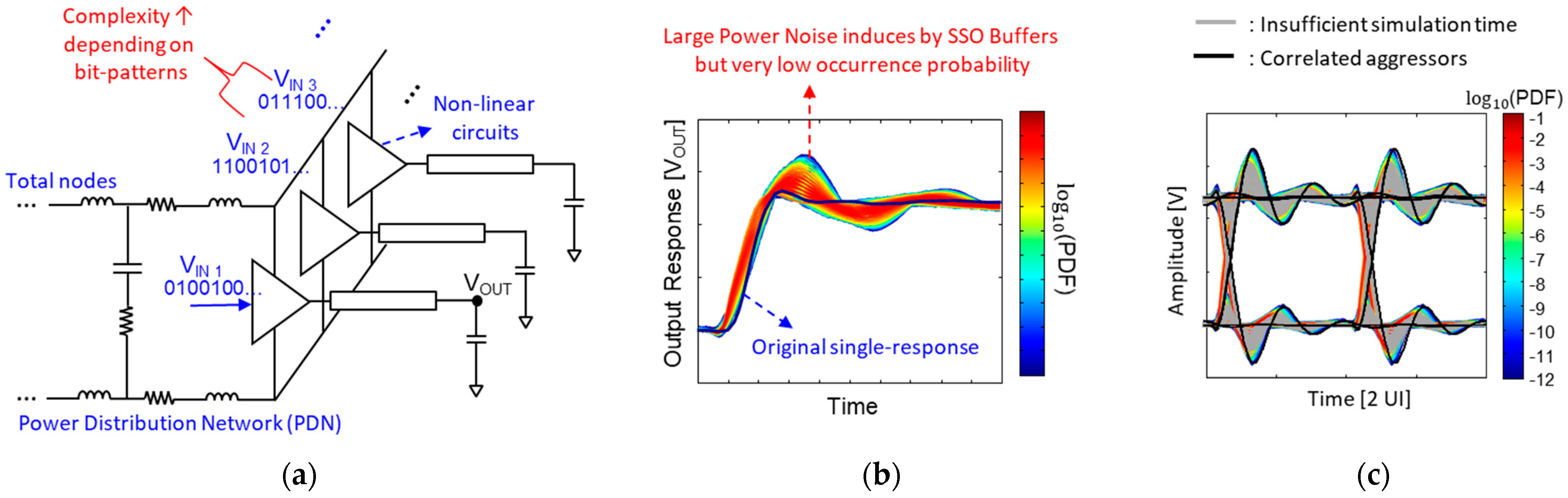
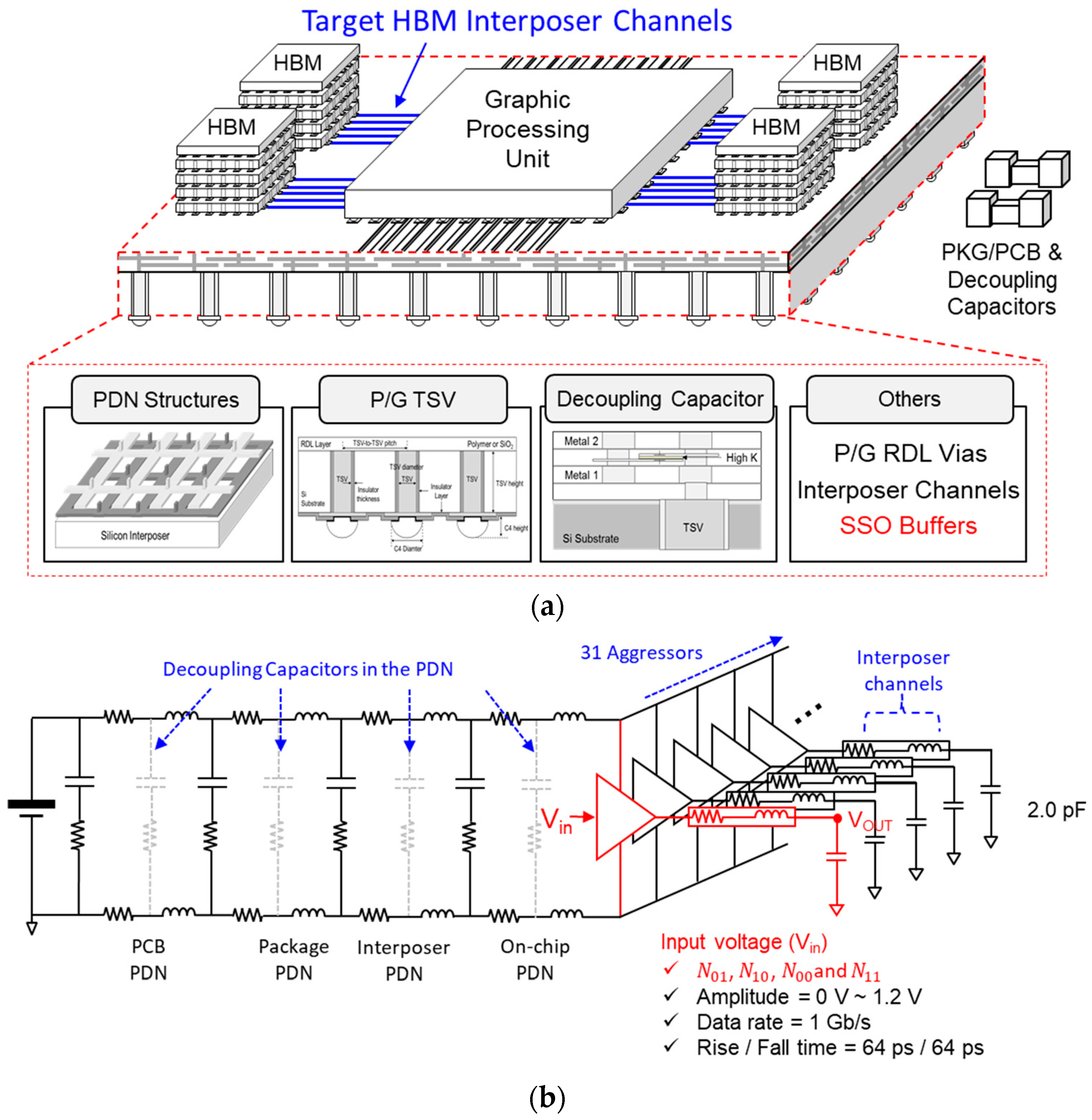
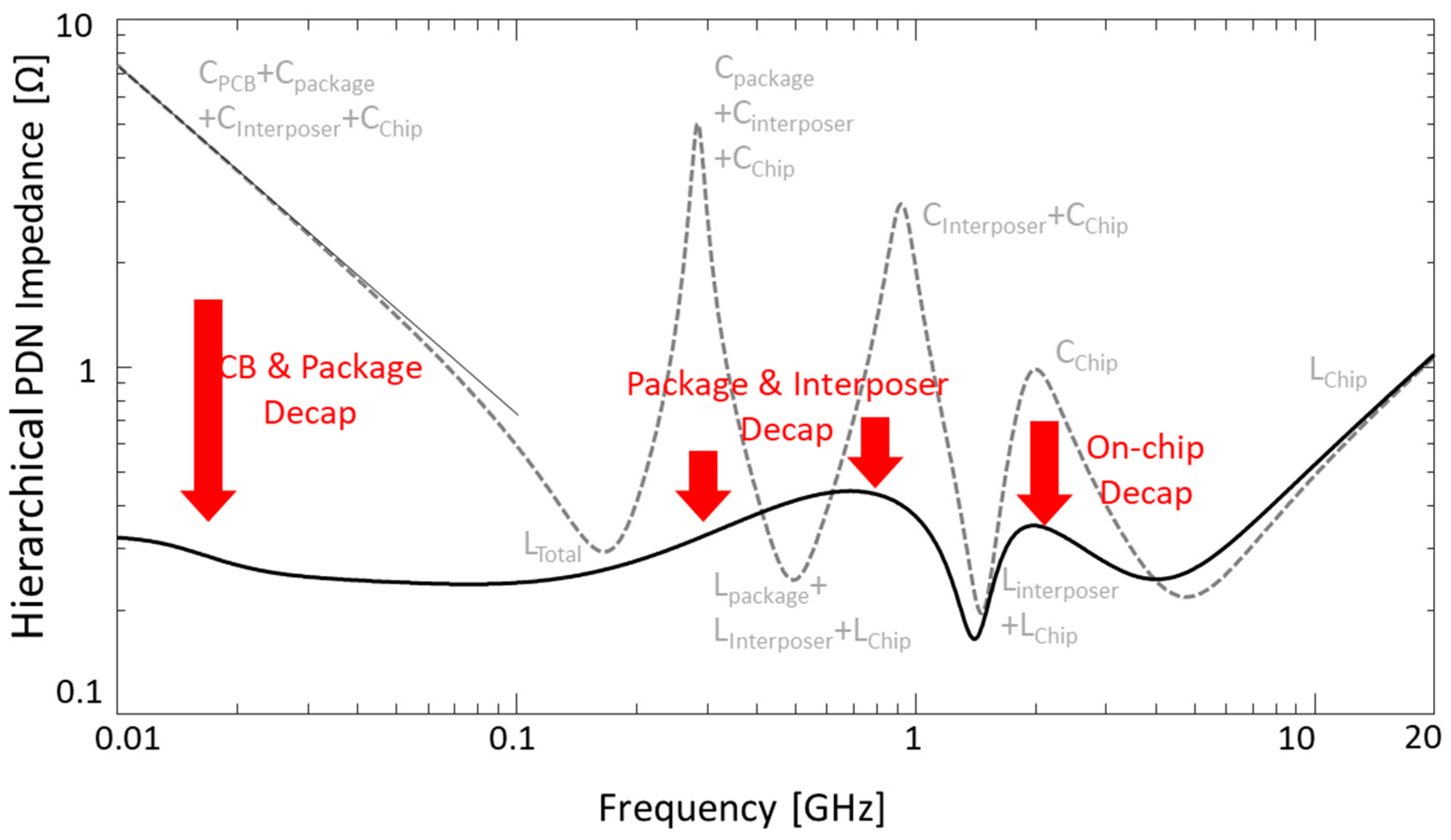
:1. Introduction
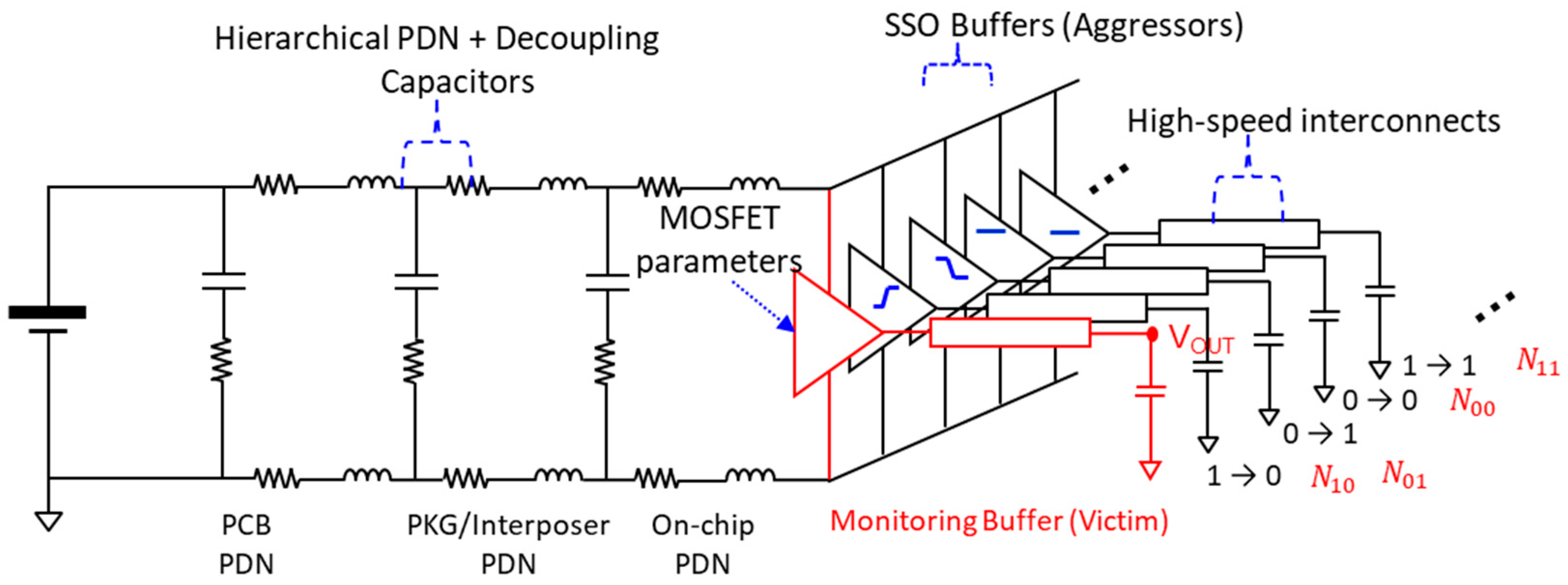
2. Statistical Eye-Diagram Estimation Method Considering Power/Ground Noise Due to SSO Buffers and Bit-Patterns
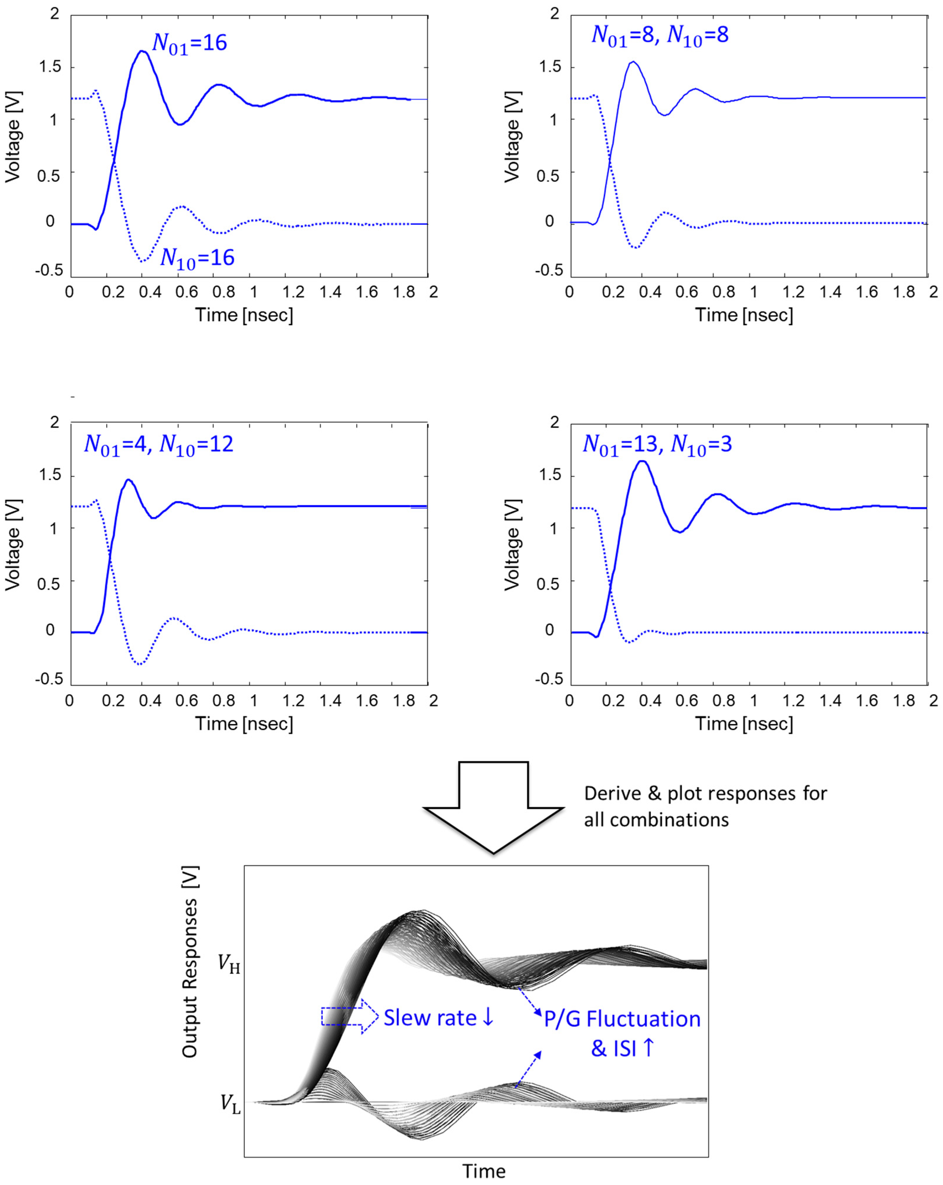
2.1. Step Responses Derivation
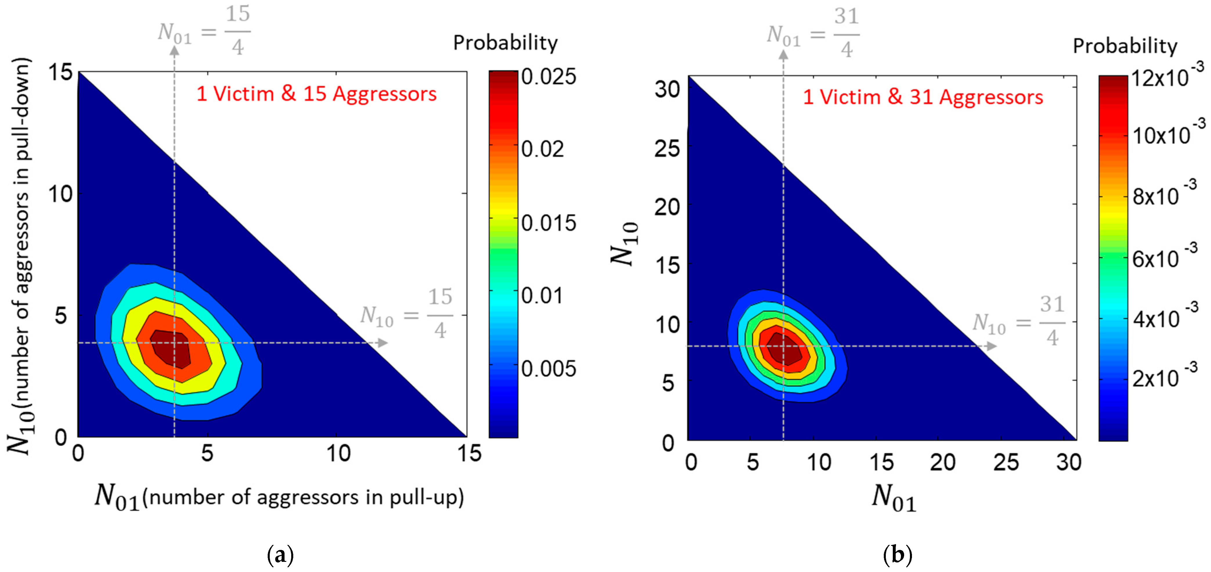
2.2. Occurrence Probability Calculation
2.2.1. Uncorrelated Buffers (Random)
2.2.2. Data Bus Inversion (DBI) Applied
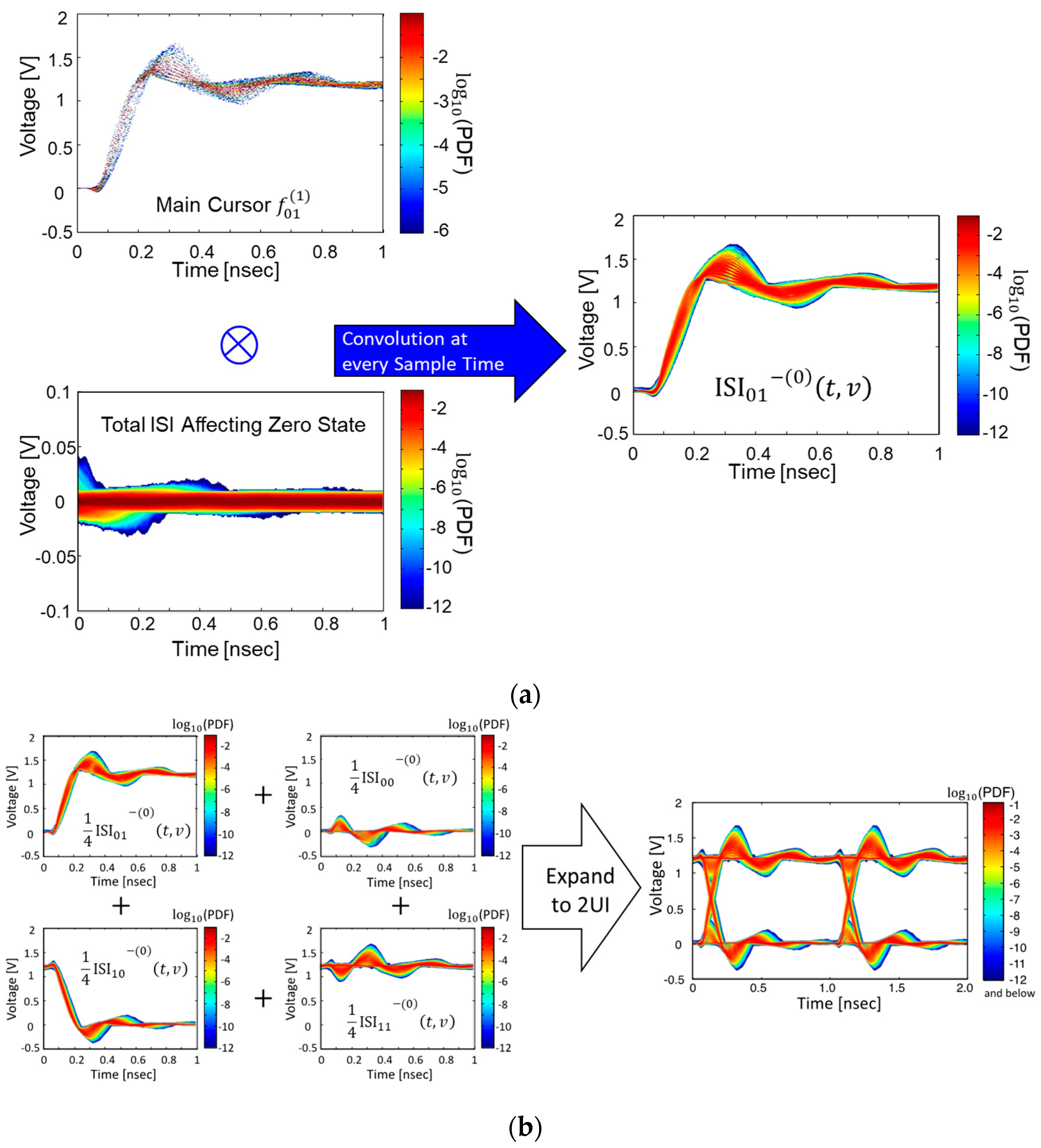
2.3. Statistical Output Responses (SORs) Derivation Based on Recursive Convolution
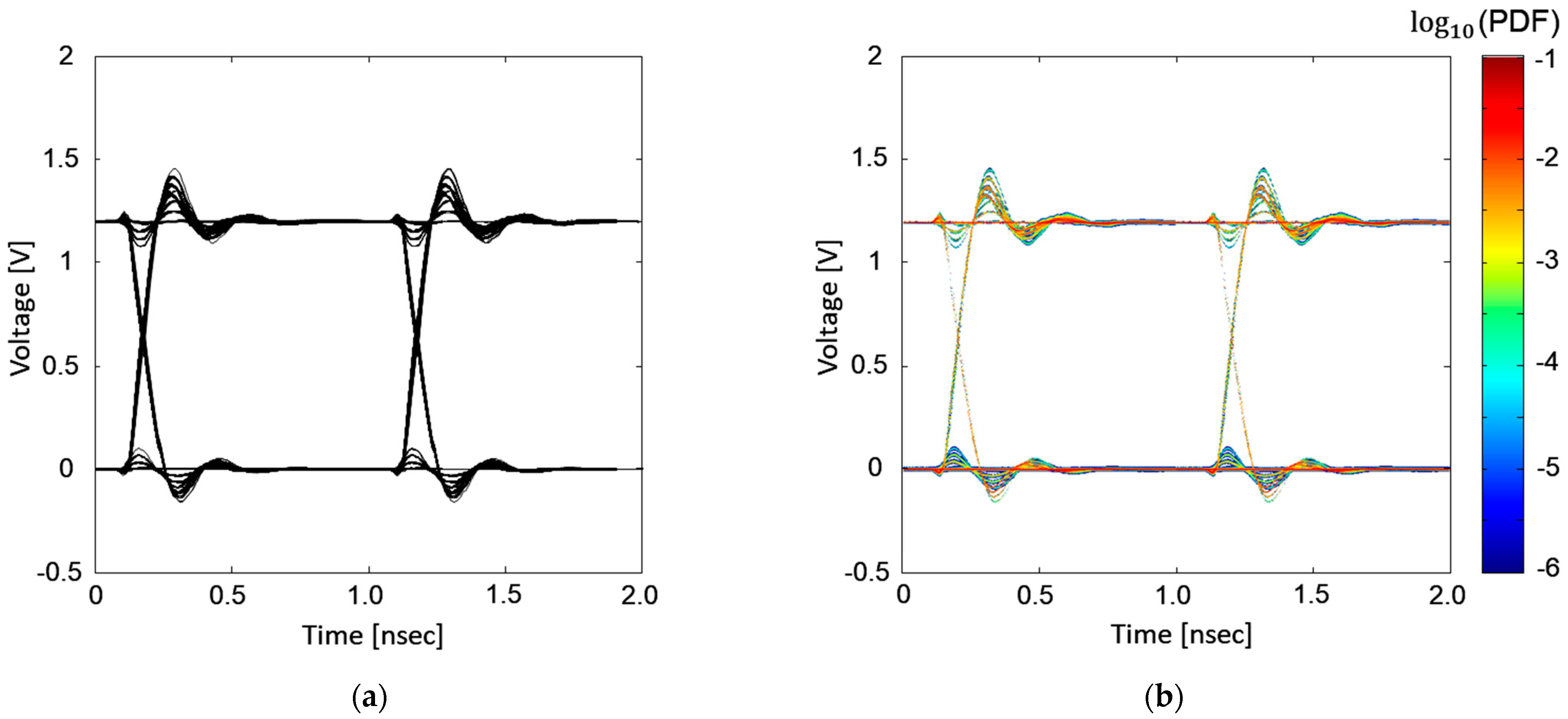
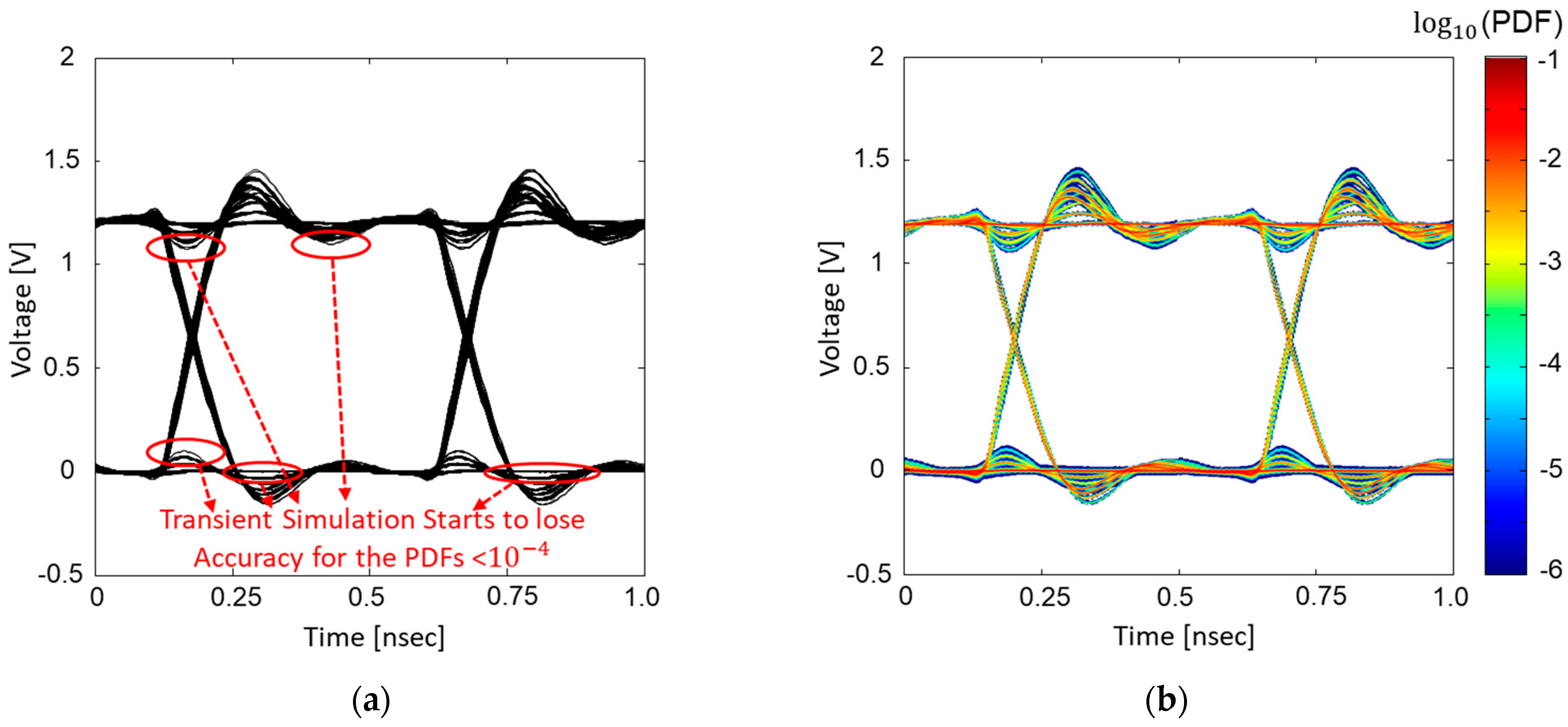
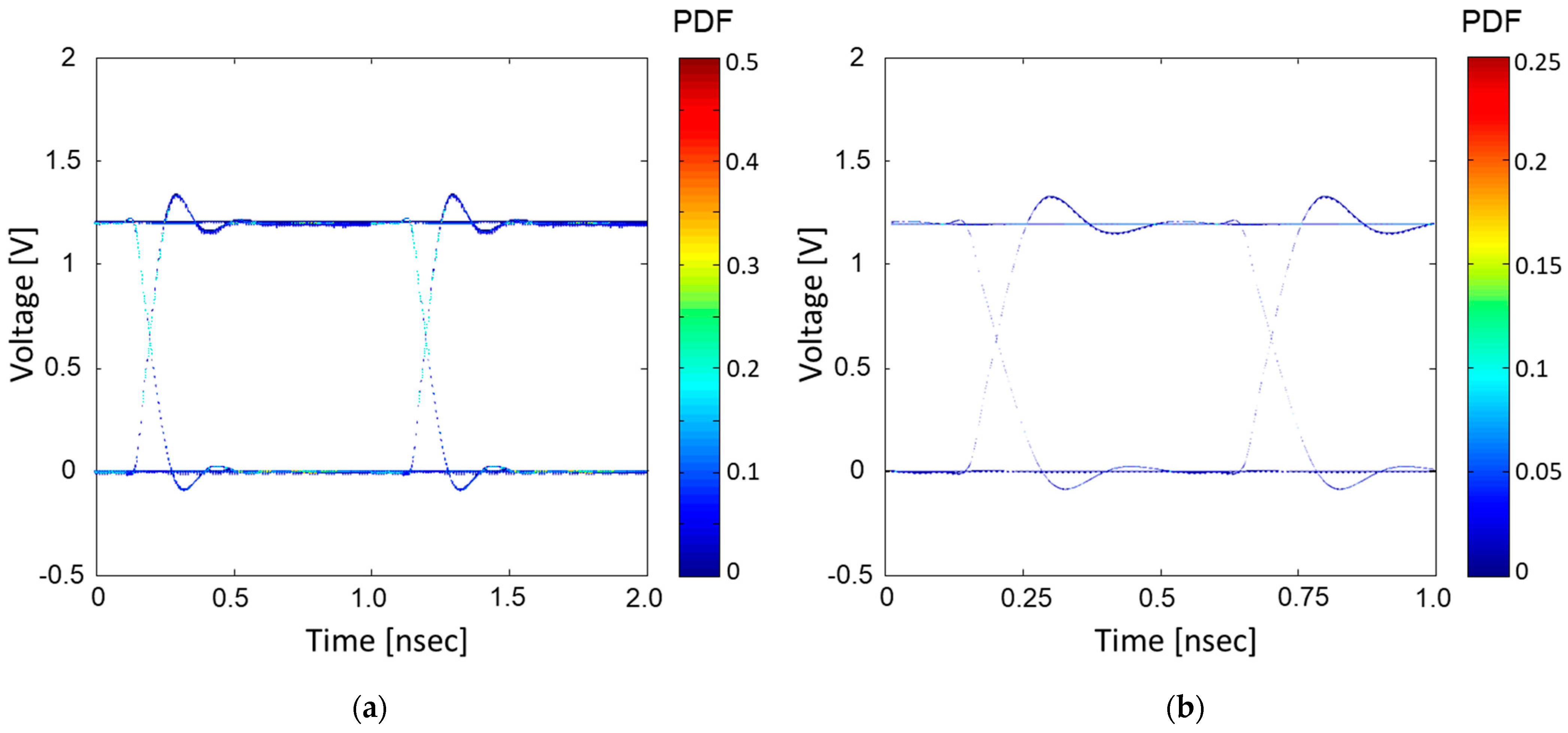
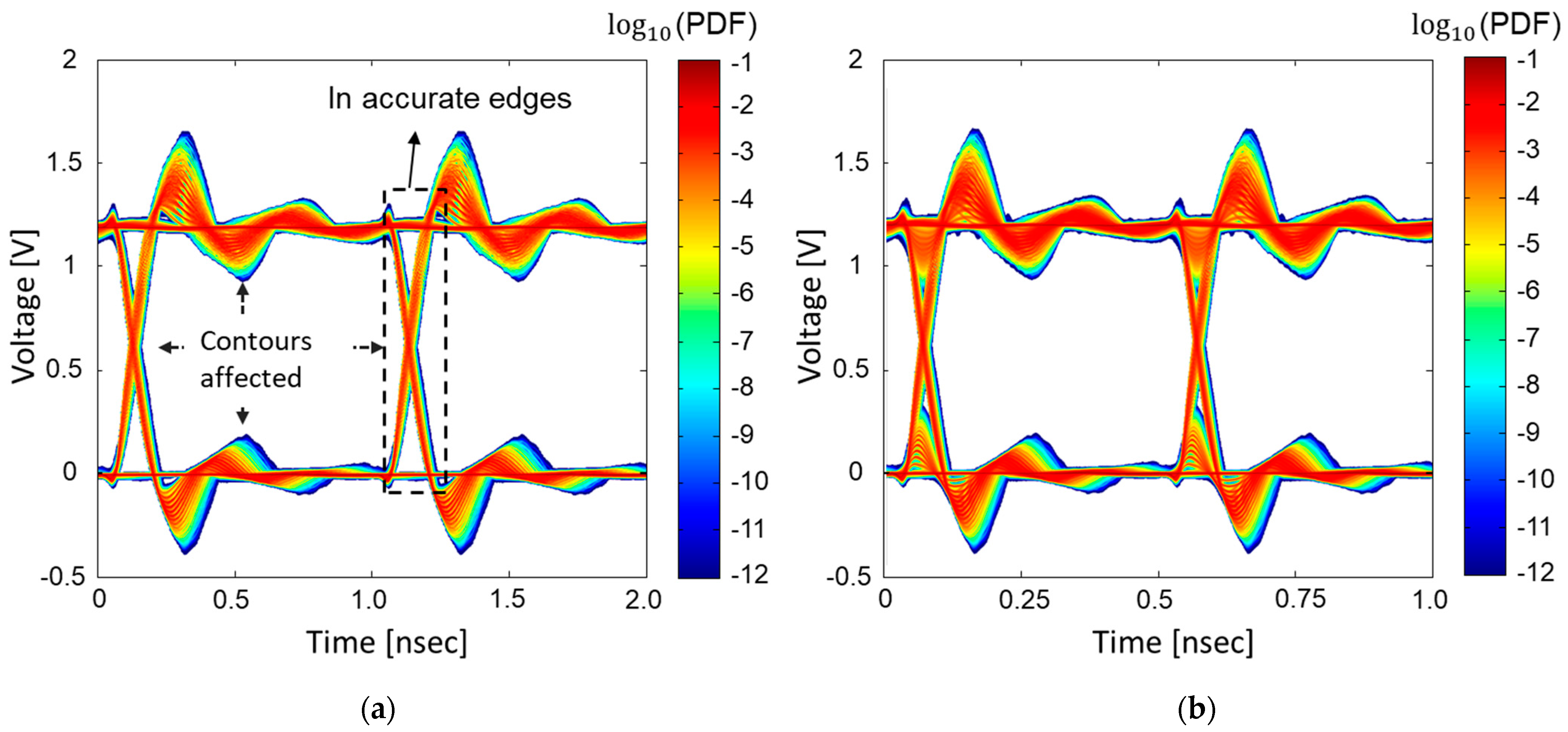
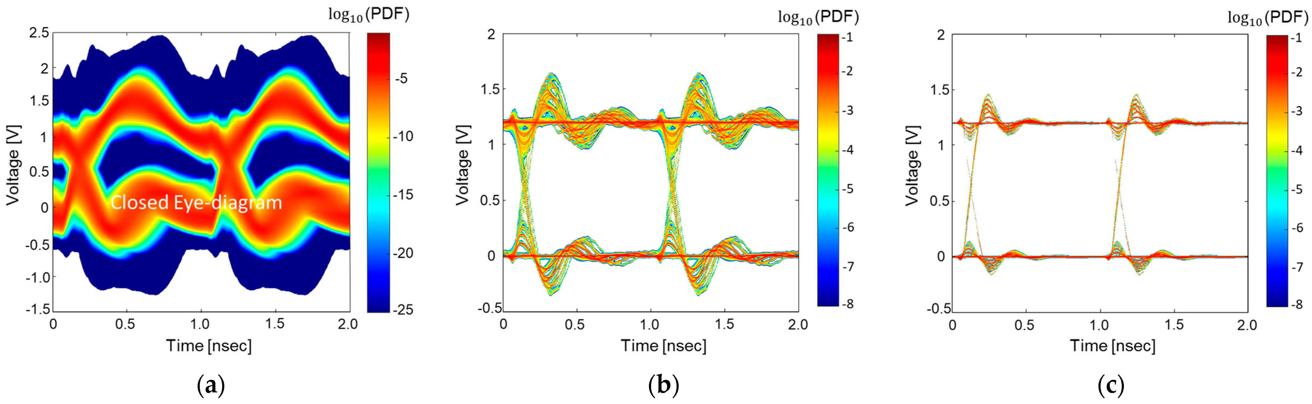
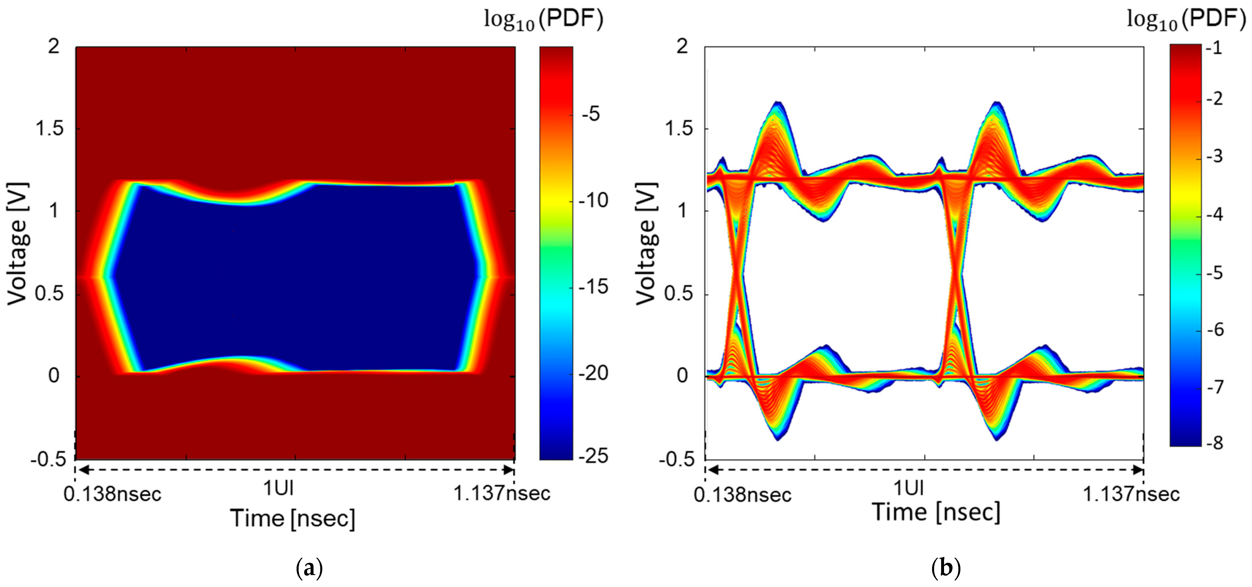
3. Verification of the Proposed Statistical Method
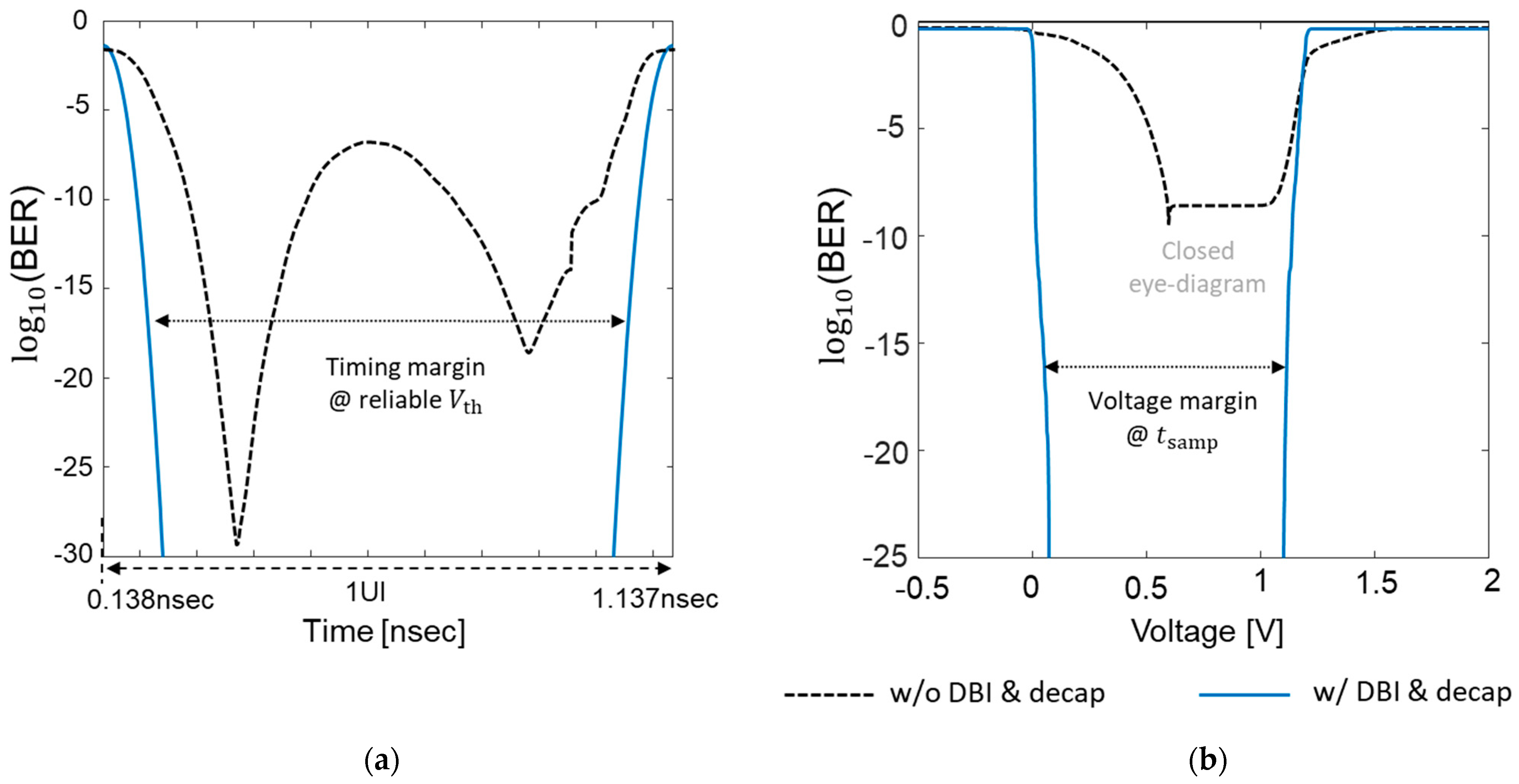
4. SI/PI Co-Design in the High-Speed Interconnect Using the Proposed Method
5. Conclusions
Funding
Conflicts of Interest
References
- JESD235A; High Bandwidth Memory (HBM) DRAM. JEDEC: Arlington, VA, USA, 2015.
- Cho, K.; Kim, Y.; Lee, H.; Kim, H.; Choi, S.; Song, J.; Kim, S.; Park, J.; Lee, S.; Kim, J. Signal Integrity Design and Analysis of Silicon Interposer for GPU-Memory Channels in High-Bandwidth Memory Interface. IEEE Trans. Compon. Packag. Manuf. Technol. 2018, 8, 1658–1671. [Google Scholar] [CrossRef]
- Cho, K.; Kim, Y.; Lee, H.; Song, J.; Park, J.; Lee, S.; Kim, S.; Park, G.; Son, K.; Kim, J. Signal Integrity Design and Analysis of Differential High-Speed Serial Links in Silicon Interposer With Through-Silicon Via. IEEE Trans. Compon. Packag. Manuf. Technol. 2018, 9, 107–121. [Google Scholar] [CrossRef]
- SK Hynix. High Bandwidth Roadmap; SK Hynix: Icheon, Republic of Korea, 2016. [Google Scholar]
- Cho, K.; Kim, Y.; Kim, S.; Park, H.; Park, J.; Lee, S.; Shim, D.; Oh, S.; Kim, J. Fast and Accurate Power Distribution Network (PDN) Modeling of A Silicon Interposer for 2.5-D/3-D ICs with Multi-array TSVs. IEEE Trans. Compon. Packag. Manuf. Technol. 2019, 9, 1835–1846. [Google Scholar] [CrossRef]
- Kim, Y.; Cho, J.; Kim, J.J.; Kim, K.; Cho, K.; Kim, S.; Sitaraman, S.; Sundaram, V.; Raj, P.M.; Tummala, R.; et al. Measurement and Analysis of Glass Interposer Power Distribution Network Resonance Effects on a High-Speed Through Glass via Channel. IEEE Trans. Electromagn. Compat. 2016, 58, 1747–1759. [Google Scholar] [CrossRef]
- Kim, H.; Lee, S.; Song, K.; Shin, Y.; Park, D.; Park, J.; Cho, J.; Ahn, S. A Novel Interposer Channel Structure with Vertical Tabbed Vias to Reduce Far-End Crosstalk for Next-Generation High-Bandwidth Memory. Micromachines 2022, 13, 1070. [Google Scholar] [CrossRef] [PubMed]
- Fan, J.; Ye, X.; Kim, J.; Archambeault, B.; Orlandi, A. Signal Integrity Design for High-Speed Digital Circuits: Progress and Directions. IEEE Trans. Electromagn. Compat. 2010, 52, 392–400. [Google Scholar] [CrossRef]
- Kim, J.; Lee, J.; Ahn, S.; Fan, J. Closed-Form Expressions for the Noise Voltage Caused by a Burst Train of IC Switching Currents on a Power Distribution Network. IEEE Trans. Electromagn. Compat. 2014, 56, 1585–1597. [Google Scholar] [CrossRef]
- Hwang, C.; Kim, J.; Achkir, B.; Fan, J. Analytical Transfer Functions Relating Power and Ground Voltage Fluctuations to Jitter at a Single-Ended Full-Swing Buffer. IEEE Trans. Compon. Packag. Manuf. Technol. 2012, 3, 113–125. [Google Scholar] [CrossRef]
- Kim, J.; Lee, J.; Cho, S.; Hwang, C.; Yoon, C.; Fan, J. Analytical Probability Density Calculation for Step Pulse Response of a Single-Ended Buffer With Arbitrary Power-Supply Voltage Fluctuations. IEEE Trans. Circuits Syst. I Regul. Pap. 2014, 61, 2022–2033. [Google Scholar] [CrossRef]
- Casper, B.K.; Haycock, M.; Mooney, R. An accurate and efficient analysis method for multi-Gb/s chip-to-chip signaling schemes. In Proceedings of the 2002 Symposium on VLSI Circuits Digest of Technical Papers, Honolulu, HI, USA, 13–15 June 2002; Volume 54, p. 57. [Google Scholar]
- Choi, S.; Kim, H.; Jung, D.H.; Kim, J.J.; Lim, J.; Kim, J. An Efficient Crosstalk-Included Eye-Diagram Estimation Method for High-Speed Interposer Channel on 2.5-D and 3-D IC. IEEE Trans. Electromagn. Compat. 2016, 59, 927–939. [Google Scholar] [CrossRef]
- Park, J.; Choi, S.; Kim, J.J.; Kim, Y.; Lee, M.; Kim, H.; Bae, B.; Song, H.; Cho, K.; Lee, S.; et al. A Novel Stochastic Model-Based Eye-Diagram Estimation Method for 8B/10B and TMDS-Encoded High-Speed Channels. IEEE Trans. Electromagn. Compat. 2017, 60, 1510–1519. [Google Scholar] [CrossRef]
- Park, J.; Jung, D.H.; Kim, B.; Choi, S.; Kim, Y.; Park, S.; Park, G.; Cho, K.; Lee, S.; Kim, J. A Novel Eye-diagram Estimation Method for Pulse Amplitude Modulation with N-Level (PAM-N) on Stacked Through-Silicon Vias (TSVs). IEEE Trans. Electromagn. Compat. 2018, 61, 1198–1206. [Google Scholar] [CrossRef]
- Chou, C.C.; Hsu, S.Y.; Wu, T.L. Estimation method for statistical eye-diagram in a non-linear digital channel. IEEE Trans. Electro-Magn. Compat. 2015, 57, 1655–1664. [Google Scholar] [CrossRef]
- Oh, D. Multiple Edge Responses for Fast and Accurate System Simulations. IEEE Trans. Adv. Packag. 2008, 31, 741–748. [Google Scholar]
- Oh, D.; Yuan, X. High-Speed Signaling: Jitter Modeling, Analysis and Budgeting, 1st ed.; Prentice Hall: Upper Saddle River, NJ, USA, 2012. [Google Scholar]
- Kim, K. Fast and Analytical Eye Diagram Estimation Method for High Bandwidth Memory (HBM) Channel Including Tx Power Noise and Channel Crosstalk. Ph.D. Dissertation, KAIST, Daejeon, Republic of Korea, 2015. [Google Scholar]
- Kim, J. Analytical Calculation of Pattern-Dependent Simultaneous Switching Outputs (SSO) due to Power Supply Fluctuations. In Proceedings of the 2015 IEEE Electrical Design of Advanced Packaging and Systems Symposium (EDAPS), Seoul, Republic of Korea, 14–16 December 2015; pp. 225–228. [Google Scholar]
- Kim, J. Statistical Analysis for Patter-Dependent Simultaneous Switching Outputs (SSO) of Parallel Single-Ended Buffers. IEEE Trans. Circuits Syst.-1 Regul. Pap. 2017, 64, 156–169. [Google Scholar] [CrossRef]
- Kim, Y.; Fujimoto, D.; Nishiyama, H.; Hayashi, Y.-I.; Lho, D.; Park, H.; Kim, J. Statistical Analysis of Simultaneous Switching Output (SSO) Impacts on Steady State Output Responses and Signal Integrity. In Proceedings of the 2019 12th International Workshop on the Electromagnetic Compatibility of Integrated Circuits (EMC Compo), Hangzhou, China, 21–23 October 2019. [Google Scholar]
- Kim, Y.; Fujimoto, D.; Kaji, S.; Wada, S.; Park, H.; Lho, D.; Kim, J.; Hayashi, Y.-I. Segmentation method based modeling and analysis of a glass package power distribution network (PDN). Nonlinear Theory Its Appl. IEICE 2020, 11, 170–188. [Google Scholar] [CrossRef]
- Cho, K.; Kim, Y.; Kim, S.; Lee, H.; Choi, S.; Kim, H.; Kim, J. Power Distribution Network (PDN) Design and Analysis of A Single and Double-Sided High Bandwidth Memory (HBM) Interposer for 2.5D Terabtye/s Bandwidth System. In Proceedings of the IEEE International Conference on Signal and Power Integrity (SIPI 2016) An embedded conference within the IEEE International Symposium on Electromagnetic Compatibility, Ottawa, ON, Canada, 27 July 2016. [Google Scholar]
- Park, H.; Park, J.; Kim, S.; Cho, K.; Lho, D.; Jeong, S.; Park, S.; Park, G.; Sim, B.; Kim, S.; et al. Deep Reinforcement Learning-Based Optimal Decoupling Capacitor Design Method for Silicon Interposer-Based 2.5-D/3-D ICs. IEEE Trans. Compon. Packag. Manuf. Technol. 2020, 10, 467–478. [Google Scholar] [CrossRef]


| Case 1 | If | If |
| Case 2 | If | If |
| Case 3 (Inversion) | If + | If + |
| Transient Simulation 1 (@BER 10−4) | The Proposed Method 2 | |||
|---|---|---|---|---|
| Eye-Height | Sim. Time | Eye-Height | Est. Time | |
| 1 Buffers, 1 Gb/s | 1.108 V | 15.81 s | 1.138 V | 3.52 s |
| 4 Buffers, 1 Gb/s | 1.063 V | 78.32 s | 1.034 V | 6.75 s |
| 4 Buffers, 2 Gb/s | 1.045 V | 80.11 s | 1.011 V | 8.10 s |
| 4 Buffers, 8 Gb/s | 0.619 V | 3487 s | 0.599 V | 26.8 s |
| 16 Buffers, 2 Gb/s | Fail to sim. | 0.701 V | 95.11 s | |
Disclaimer/Publisher’s Note: The statements, opinions and data contained in all publications are solely those of the individual author(s) and contributor(s) and not of MDPI and/or the editor(s). MDPI and/or the editor(s) disclaim responsibility for any injury to people or property resulting from any ideas, methods, instructions or products referred to in the content. |
© 2023 by the author. Licensee MDPI, Basel, Switzerland. This article is an open access article distributed under the terms and conditions of the Creative Commons Attribution (CC BY) license (https://creativecommons.org/licenses/by/4.0/).
Share and Cite
Kim, Y. A Statistical Approach for Signal and Power Integrity Co-Design in High-Speed Interconnects Considering Non-Linear Power/Ground Noise and Bit-Patterns. Micromachines 2023, 14, 1654. https://doi.org/10.3390/mi14091654
Kim Y. A Statistical Approach for Signal and Power Integrity Co-Design in High-Speed Interconnects Considering Non-Linear Power/Ground Noise and Bit-Patterns. Micromachines. 2023; 14(9):1654. https://doi.org/10.3390/mi14091654
Chicago/Turabian StyleKim, Youngwoo. 2023. "A Statistical Approach for Signal and Power Integrity Co-Design in High-Speed Interconnects Considering Non-Linear Power/Ground Noise and Bit-Patterns" Micromachines 14, no. 9: 1654. https://doi.org/10.3390/mi14091654
APA StyleKim, Y. (2023). A Statistical Approach for Signal and Power Integrity Co-Design in High-Speed Interconnects Considering Non-Linear Power/Ground Noise and Bit-Patterns. Micromachines, 14(9), 1654. https://doi.org/10.3390/mi14091654