
A Highly Efficient Electromagnetic Wave Absorption System with Graphene Embedded in Hybrid Perovskite

 ,
,
Abstract
:1. Introduction
2. Materials and Methods
2.1. Materials
2.2. Synthesis of MPI/Graphene Composites
2.3. Characterization
3. Results and Discussion
4. Conclusions
Supplementary Materials
Author Contributions
Funding
Data Availability Statement
Conflicts of Interest
References
- Zeng, X.; Zhao, C.; Jiang, X.; Yu, R.; Che, R. Functional Tailoring of Multi-Dimensional Pure MXene Nanostructures for Significantly Accelerated Electromagnetic Wave Absorption. Small 2023, e2303393. [Google Scholar] [CrossRef] [PubMed]
- Wang, Y.; Yao, L.; Zheng, Q.; Cao, M.-S. Graphene-wrapped multiloculated nickel ferrite: A highly efficient electromagnetic attenuation material for microwave absorbing and green shielding. Nano Res. 2022, 15, 6751–6760. [Google Scholar] [CrossRef]
- Cao, M.; Han, C.; Wang, X.; Zhang, M.; Zhang, Y.; Shu, J.; Yang, H.; Fang, X.; Yuan, J. Graphene nanohybrids: Excellent electromagnetic properties for the absorbing and shielding of electromagnetic waves. J. Mater. Chem. C 2018, 6, 4586–4602. [Google Scholar] [CrossRef]
- Wang, F.; Gu, W.; Chen, J.; Wu, Y.; Zhou, M.; Tang, S.; Cao, X.; Zhang, P.; Ji, G. The point defect and electronic structure of K doped LaCo0.9Fe0.1O3 perovskite with enhanced microwave absorbing ability. Nano Res. 2021, 15, 3720–3728. [Google Scholar] [CrossRef]
- Miao, P.; Yang, J.; Liu, Y.; Xie, H.; Chen, K.-J.; Kong, J. Emerging Perovskite Electromagnetic Wave Absorbers from Bi-Metal–Organic Frameworks. Cryst. Growth Des. 2020, 20, 4818–4826. [Google Scholar] [CrossRef]
- Miao, P.; Qu, N.; Chen, W.; Wang, T.; Zhao, W.; Kong, J. A two-dimensional semiconductive Cu-S metal-organic framework for broadband microwave absorption. Chem. Eng. J. 2023, 454, 140445. [Google Scholar] [CrossRef]
- Zhang, Z.; Yao, Y.; Zhang, J.; Ma, Y.; Xu, P.; Zhang, P.; Yang, Z.; Zhou, W. Two-dimensional (PEA)2PbBr4 perovskite modified with conductive network for high-performance electromagnetic wave absorber. Mater. Lett. 2022, 326, 132926. [Google Scholar] [CrossRef]
- Zhang, Z.; Xiong, Z.; Yao, Y.; Wang, D.; Yang, Z.; Zhang, P.; Zhao, Q.; Zhou, W. Constructing Conductive Network in Hybrid Perovskite for a Highly Efficient Microwave Absorption System. Adv. Funct. Mater. 2022, 32, 2206053. [Google Scholar] [CrossRef]
- Zhang, Z.; Xiong, Z.; Yao, Y.; Shi, X.; Zhang, P.; Yang, Z.; Zhao, Q.; Zhou, W. Inorganic Halide Perovskite Electromagnetic Wave Absorption System with Ultra-Wide Absorption Bandwidth and High Thermal-Stability. Adv. Electron. Mater. 2022, 9, 2201179. [Google Scholar] [CrossRef]
- Qin, F.; Chen, J.; Liu, J.; Liu, L.; Tang, C.; Tang, B.; Li, G.; Zeng, L.; Li, H.; Yi, Z. Design of high efficiency perovskite solar cells based on inorganic and organic undoped double hole layer. Sol. Energy 2023, 262, 111796. [Google Scholar] [CrossRef]
- Guo, H.; Yang, J.; Pu, B.; Chen, H.; Li, Y.; Wang, Z.; Niu, X. Excellent microwave absorption of lead halide perovskites with high stability. J. Mater. Chem. C 2018, 6, 4201–4207. [Google Scholar] [CrossRef]
- Lai, R.; Shi, P.; Yi, Z.; Li, H.; Yi, Y. Triple-Band Surface Plasmon Resonance Metamaterial Absorber Based on Open-Ended Prohibited Sign Type Monolayer Graphene. Micromachines 2023, 14, 953. [Google Scholar] [CrossRef]
- Chen, Z.; Cai, P.; Wen, Q.; Chen, H.; Tang, Y.; Yi, Z.; Wei, K.; Li, G.; Tang, B.; Yi, Y. Graphene Multi-Frequency Broadband and Ultra-Broadband Terahertz Absorber Based on Surface Plasmon Resonance. Electronics 2023, 12, 2655. [Google Scholar] [CrossRef]
- Tong, Y.; He, M.; Zhou, Y.; Nie, S.; Zhong, X.; Fan, L.; Huang, T.; Liao, Q.; Wang, Y. Three-Dimensional Hierarchical Architecture of the TiO2/Ti3C2Tx/RGO Ternary Composite Aerogel for Enhanced Electromagnetic Wave Absorption. ACS Sustain. Chem. Eng. 2018, 6, 8212–8222. [Google Scholar] [CrossRef]
- Feng, J.; Hou, Y.; Wang, Y.; Li, L. Synthesis of Hierarchical ZnFe2O4@SiO2@RGO Core-Shell Microspheres for Enhanced Electromagnetic Wave Absorption. ACS Appl. Mater. Interfaces 2017, 9, 14103–14111. [Google Scholar] [CrossRef] [PubMed]
- Wang, M.; Lin, M.; Li, J.; Huang, L.; Zhuang, Z.; Lin, C.; Zhou, L.; Mai, L. Metal-organic framework derived carbon-confined Ni2P nanocrystals supported on graphene for an efficient oxygen evolution reaction. Chem. Commun. 2017, 53, 8372–8375. [Google Scholar] [CrossRef] [PubMed]
- Han, M.; Yin, X.; Kong, L.; Li, M.; Duan, W.; Zhang, L.; Cheng, L. Graphene-wrapped ZnO hollow spheres with enhanced electromagnetic wave absorption properties. J. Mater. Chemisry A 2014, 2, 16403–16409. [Google Scholar] [CrossRef]
- Sun, X.; He, J.; Li, G.; Tang, J.; Wang, T.; Guo, Y.; Xue, H. Laminated magnetic graphene with enhanced electromagnetic wave absorption properties. J. Mater. Chemisry C 2013, 1, 765–777. [Google Scholar] [CrossRef]
- Zhang, C.; Chen, G.; Zhang, R.; Wu, Z.; Xu, C.; Man, H.; Che, R. Charge modulation of CNTs-based conductive network for oxygen reduction reaction and microwave absorption. Carbon 2021, 178, 310–319. [Google Scholar] [CrossRef]
- Hu, Q.; Yang, R.; Mo, Z.; Lu, D.; Yang, L.; He, Z.; Zhu, H.; Tang, Z.; Gui, X. Nitrogen-doped and Fe-filled CNTs/NiCo2O4 porous sponge with tunable microwave absorption performance. Carbon 2019, 153, 737–744. [Google Scholar] [CrossRef]
- Gao, Z.; Zhao, Z.; Lan, D.; Kou, K.; Zhang, J.; Wu, H. Accessory ligand strategies for hexacyanometallate networks deriving perovskite polycrystalline electromagnetic absorbents. J. Mater. Sci. Technol. 2021, 82, 69–79. [Google Scholar] [CrossRef]
- Wang, K.; Zhang, S.; Chu, W.; Li, H.; Chen, Y.; Chen, B.; Chen, B.; Liu, H. Tailoring conductive network nanostructures of ZIF-derived cobalt-decorated N-doped graphene/carbon nanotubes for microwave absorption applications. J. Colloid Interface Sci. 2021, 591, 463–473. [Google Scholar] [CrossRef] [PubMed]
- Wang, R.; Yang, E.; Qi, X.; Xie, R.; Qin, S.; Deng, C.; Zhong, W. Constructing and optimizing core@shell structure CNTs@MoS2 nanocomposites as outstanding microwave absorbers. Appl. Surf. Sci. 2020, 516, 146159. [Google Scholar] [CrossRef]
- Wu, F.; Shi, P.; Yi, Z.; Li, H.; Yi, Y. Ultra-Broadband Solar Absorber and High-Efficiency Thermal Emitter from UV to Mid-Infrared Spectrum. Micromachines 2023, 14, 985. [Google Scholar] [CrossRef]
- Zheng, Y.; Yi, Z.; Liu, L.; Wu, X.; Liu, H.; Li, G.; Zeng, L.; Li, H.; Wu, P. Numerical simulation of efficient solar absorbers and thermal emitters based on multilayer nanodisk arrays. Appl. Therm. Eng. 2023, 230, 120841. [Google Scholar] [CrossRef]
- Liang, S.; Xu, F.; Li, W.; Yang, W.; Cheng, S.; Yang, H.; Chen, J.; Yi, Z.; Jiang, P. Tunable smart mid infrared thermal control emitter based on phase change material VO2 thin film. Appl. Therm. Eng. 2023, 232, 121074. [Google Scholar] [CrossRef]
- Weir, W.B. Automatic Measurement of Complex Dielectric Constant and Permeability at Microwave Frequencie. Proc. IEEE 1974, 62, 33–36. [Google Scholar] [CrossRef]
- Nicolson, A.M.; Ross, G.F. Measurement of the Intrinsic Properties of materials by Time-Domain Techniques. IEEE Transsactions Instrum. Meas. 1970, 19, 377–382. [Google Scholar]
- Liu, Y.; Yang, Z.; Cui, D.; Ren, X.; Sun, J.; Liu, X.; Zhang, J.; Wei, Q.; Fan, H.; Yu, F.; et al. Two-Inch-Sized Perovskite CH3 NH3PbX3 (X = Cl, Br, I) Crystals: Growth and Characterization. Adv. Mater. 2015, 27, 5176–5183. [Google Scholar] [CrossRef]
- Zhang, C.; Mu, C.; Xiang, J.; Wang, B.; Wen, F.; Song, J.; Wang, C.; Liu, Z. Microwave absorption characteristics of CH3NH3PbI3 perovskite/carbon nanotube composites. J. Mater. Sci. 2017, 52, 13023–13032. [Google Scholar] [CrossRef]
- Chang, S.; Chen, C.; Chen, L.; Tien, C.; Cheng, H.; Huang, W.; Lin, H.; Chen, S.; Wu, G. Unraveling the multifunctional capabilities of PCBM thin films in inverted-type CH3NH3PbI3 based photovoltaics. Sol. Energy Mater. Sol. Cells 2017, 169, 40–46. [Google Scholar] [CrossRef]
- Chen, X.; Xu, Y.; Wang, Z.; Wu, R.J.; Cheng, H.L.; Chui, H.C. Characterization of a CH3NH3PbI3 perovskite microwire by Raman spectroscopy. J. Raman Spectrosc. 2022, 53, 288–296. [Google Scholar] [CrossRef]
- Pérez-Osorio, M.A.; Milot, R.L.; Filip, M.R.; Patel, J.B.; Herz, L.M.; Johnston, M.B.; Giustino, F. Vibrational Properties of the Organic–Inorganic Halide Perovskite CH3NH3PbI3 from Theory and Experiment: Factor Group Analysis, First-Principles Calculations, and Low-Temperature Infrared Spectra. J. Phys. Chem. C 2015, 119, 25703–25718. [Google Scholar] [CrossRef]
- Jia, X.; Hu, Z.; Zhu, Y.; Weng, T.; Wang, J.; Zhang, J.; Zhu, Y. Facile synthesis of organic–inorganic hybrid perovskite CH3NH3PbI3 microcrystals. J. Alloys Compd. 2017, 725, 270–274. [Google Scholar] [CrossRef]
- Zhang, Z.; Lv, X.; Chen, Y.; Zhang, P.; Sui, M.; Liu, H.; Sun, X. NiS2@MoS2 Nanospheres Anchored on Reduced Graphene Oxide: A Novel Ternary Heterostructure with Enhanced Electromagnetic Absorption Property. Nanomaterials 2019, 9, 292. [Google Scholar] [CrossRef]
- Tseng, W.S.; Jao, M.H.; Hsu, C.C.; Huang, J.S.; Wu, C.I.; Yeh, N.C. Stabilization of hybrid perovskite CH3NH3PbI3 thin films by graphene passivation. Nanoscale 2017, 9, 19227–19235. [Google Scholar] [CrossRef] [PubMed]
- Li, Y.; Xu, X.; Wang, C.; Ecker, B.; Yang, J.; Huang, J.; Gao, Y. Light-Induced Degradation of CH3NH3PbI3 Hybrid Perovskite Thin Film. J. Phys. Chem. C 2017, 121, 3904–3910. [Google Scholar] [CrossRef]
- Yang, W.; Ni, M.; Ren, X.; Tian, Y.; Li, N.; Su, Y.; Zhang, X. Graphene in Supercapacitor Applications. Curr. Opin. Colloid Interface Sci. 2015, 20, 416–428. [Google Scholar] [CrossRef]
- Quan, B.; Liang, X.; Xu, G.; Cheng, Y.; Zhang, Y.; Liu, W.; Ji, G.; Du, Y. A permittivity regulating strategy to achieve high-performance electromagnetic wave absorbers with compatibility of impedance matching and energy conservation. New J. Chem. 2017, 41, 1259–1266. [Google Scholar] [CrossRef]
- Zhao, B.; Shao, G.; Fan, B.; Zhao, W.; Zhang, R. Investigation of the electromagnetic absorption properties of Ni@TiO2 and Ni@SiO2 composite microspheres with core-shell structure. Phys. Chem. Chem. Phys. 2015, 17, 2531–2539. [Google Scholar] [CrossRef]
- Xie, A.; Sun, M.; Zhang, K.; Jiang, W.; Wu, F.; He, M. In situ growth of MoS2 nanosheets on reduced graphene oxide (RGO) surfaces: Interfacial enhancement of absorbing performance against electromagnetic pollution. Phys. Chem. Chem. Phys. 2016, 18, 24931–24936. [Google Scholar] [CrossRef] [PubMed]
- Sun, X.; Yuan, X.; Li, X.; Li, L.; Song, Q.; Lv, X.; Gu, G.; Sui, M. Hollow cube-like CuS derived from Cu2O crystals for the highly efficient elimination of electromagnetic pollution. New J. Chem. 2018, 42, 6735–6741. [Google Scholar] [CrossRef]
- Wang, Y.; Han, X.; Xu, P.; Liu, D.; Cui, L.; Zhao, H.; Du, Y. Synthesis of pomegranate-like Mo2C@C nanospheres for highly efficient microwave absorption. Chem. Eng. J. 2019, 372, 312–320. [Google Scholar] [CrossRef]
- Cheng, Y.; Li, Z.; Li, Y.; Dai, S.; Ji, G.; Zhao, H.; Cao, J.; Du, Y. Rationally regulating complex dielectric parameters of mesoporous carbon hollow spheres to carry out efficient microwave absorption. Carbon 2018, 127, 643–652. [Google Scholar] [CrossRef]
- Zhao, B.; Shao, G.; Fan, B.; Zhao, W.; Xie, Y.; Zhang, R. Facile preparation and enhanced microwave absorption properties of core-shell composite spheres composited of Ni cores and TiO2 shells. Phys. Chem. Chem. Phys. PCCP 2015, 17, 8802–8810. [Google Scholar] [CrossRef]


| MPI Precursor Solution (mL) | Graphene Suspension (mL) | MPI/Graphene | Sample Number |
|---|---|---|---|
| 0.806 | 2.4 | 24:1 | MG-1 |
| 0.806 | 3.75 | 16:1 | MG-2 |
| 0.806 | 4.95 | 12:1 | MG-3 |
| 0.806 | 7.5 | 8:1 | MG-4 |
| 0.806 | 9.9 | 6:1 | MG-5 |
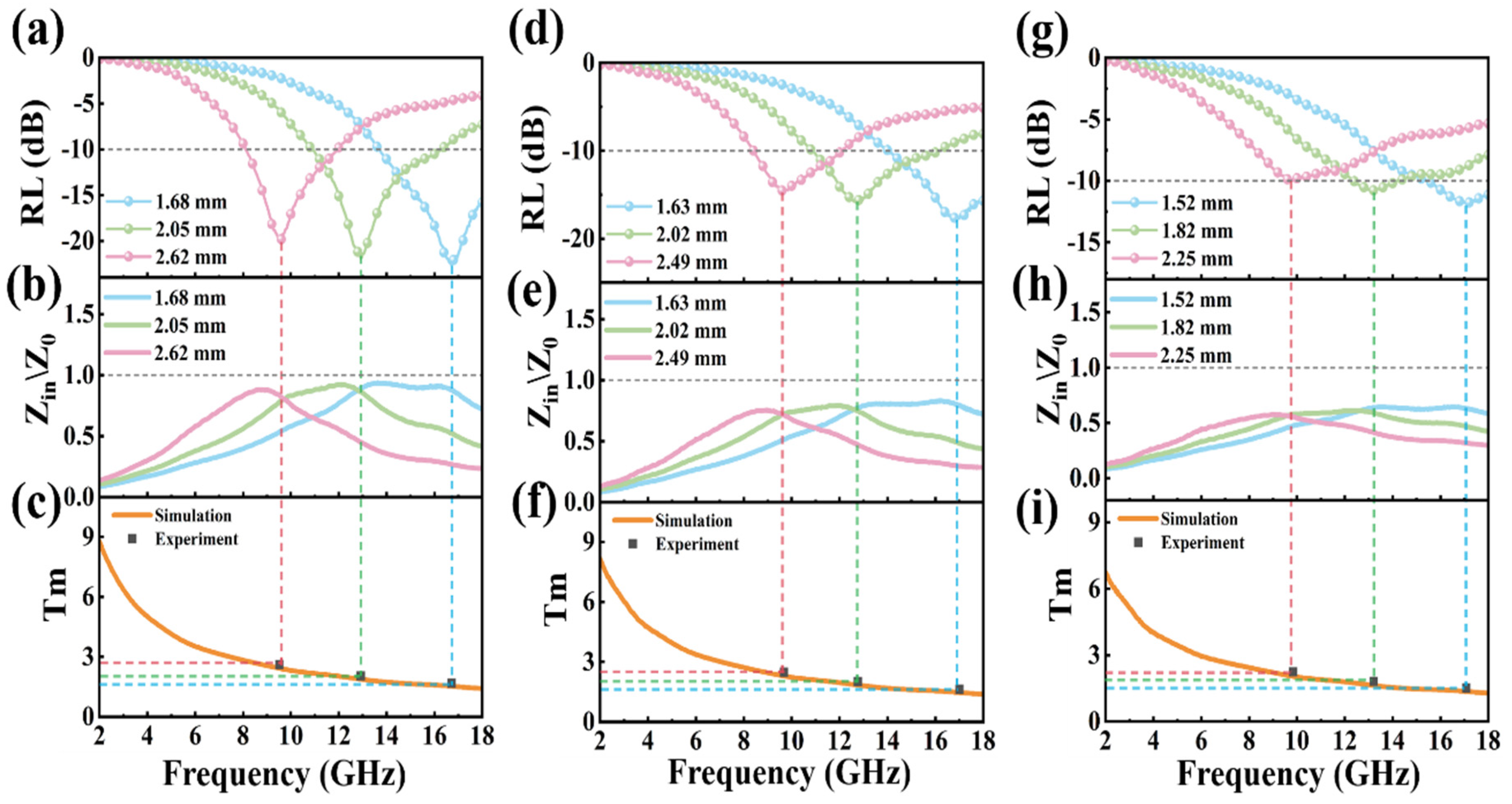
| Sample | Point | (dB) | (mm) | (GHz) |
|---|---|---|---|---|
| MG-1 | 22.69 | 1.68 | 16.72 | |
| 21.88 | 2.05 | 12.92 | ||
| 19.93 | 2.62 | 9.52 | ||
| MG-2 | 17.68 | 1.63 | 17.00 | |
| 15.74 | 2.02 | 12.76 | ||
| 14.53 | 2.49 | 9.68 | ||
| MG-3 | 11.75 | 1.52 | 17.08 | |
| 10.78 | 1.82 | 13.20 | ||
| 9.97 | 2.25 | 9.84 |
Disclaimer/Publisher’s Note: The statements, opinions and data contained in all publications are solely those of the individual author(s) and contributor(s) and not of MDPI and/or the editor(s). MDPI and/or the editor(s) disclaim responsibility for any injury to people or property resulting from any ideas, methods, instructions or products referred to in the content. |
© 2023 by the authors. Licensee MDPI, Basel, Switzerland. This article is an open access article distributed under the terms and conditions of the Creative Commons Attribution (CC BY) license (https://creativecommons.org/licenses/by/4.0/).
Share and Cite
Yu, H.; Liu, H.; Yao, Y.; Xiong, Z.; Gao, L.; Yang, Z.; Zhou, W.; Zhang, Z. A Highly Efficient Electromagnetic Wave Absorption System with Graphene Embedded in Hybrid Perovskite. Micromachines 2023, 14, 1611. https://doi.org/10.3390/mi14081611
Yu H, Liu H, Yao Y, Xiong Z, Gao L, Yang Z, Zhou W, Zhang Z. A Highly Efficient Electromagnetic Wave Absorption System with Graphene Embedded in Hybrid Perovskite. Micromachines. 2023; 14(8):1611. https://doi.org/10.3390/mi14081611
Chicago/Turabian StyleYu, Haitao, Hui Liu, Yao Yao, Ziming Xiong, Lei Gao, Zhiqian Yang, Wenke Zhou, and Zhi Zhang. 2023. "A Highly Efficient Electromagnetic Wave Absorption System with Graphene Embedded in Hybrid Perovskite" Micromachines 14, no. 8: 1611. https://doi.org/10.3390/mi14081611
APA StyleYu, H., Liu, H., Yao, Y., Xiong, Z., Gao, L., Yang, Z., Zhou, W., & Zhang, Z. (2023). A Highly Efficient Electromagnetic Wave Absorption System with Graphene Embedded in Hybrid Perovskite. Micromachines, 14(8), 1611. https://doi.org/10.3390/mi14081611