1. Introduction
With a wide bandgap of ≈3.27 eV at 300 K, 4H-SiC, a polytype of silicon carbide, offers very low leakage current as a rectifying device even at high reverse bias resulting in extremely low thermal noise [
1,
2,
3,
4,
5]. The dielectric constant of 4H-SiC (9.7) is much lower when compared to 11.9 and 16.0 in Si and Ge, respectively, which helps to lower the detector capacitance for a given detector active volume. The lower detector capacitance in turn helps to achieve higher charge collection efficiency and lower the white series noise [
6]. Epitaxially grown 4H-SiC layers exhibit excellent electron transport properties, including high drift mobility (≈1000 cm
2/V/s), which allows faster charge collection and hence provides fast response time. 4H-SiC epilayer devices also demonstrate high breakdown electric field (3 × 10
6 V/cm), a saturation electron drift velocity (2 × 10
7 cm/s) twice that of silicon, and a relatively low electron-hole pair (ehp) generation energy of 7.28 eV. Lower ehp generation energy implies a large Fano factor and thereby a high energy resolution [
5,
7,
8]. A high sublimation point of 2857 °C and thermal conductivity of 280 W/m/K allows 4H-SiC devices and ICs to operate at temperatures as high as 800 °C [
9]. A high displacement threshold of Si (35 eV) and C (22 eV) in 4H-SiC makes it difficult for incident radiations to displace any atom from its lattice point, making it radiation hard and hence suitable for applications in environments with high background radiation [
10,
11]. Due to the above-mentioned superior electronic properties along with its physical ruggedness, 4H-SiC has been demonstrated to be compatible with harsh environment applications such as in nuclear reactor cores, laser plasma, space missions, and high energy astrophysics [
12,
13,
14].
Despite the promising aforementioned properties, a wide variety of microscopic and macroscopic crystal defects exist in the state-of-the-art 4H-SiC wafers which deteriorate the device performance [
15,
16]. In particular, micropipe defects in 4H-SiC single crystals, which are basically hollow-core threading screw dislocations, are the most potential crystal defects that deteriorate the device performance [
17,
18]. As a result, over the last decade, much effort has been put into reducing the micropipe defect concentration. Nowadays, 4H-SiC epitaxial layers are regularly grown with micropipe defect density < 1 cm
−2 [
19]. Microscopic trap centers, such as deep levels related to point defects, trap charge carriers, thereby adversely affecting the charge collection and detector performance [
20,
21]. Semiconductor devices with lower defect concentrations have a higher mobility-lifetime (
μτ) product, a figure-of-merit for charge transport properties, and exhibit higher energy resolution. Among the best detectors, the concentration of the point defects is reported to be below 10
12 cm
−3 [
22,
23,
24]. Among various reported point defects in 4H-SiC, the most significant is the Z
1/2 “electron lifetime killing” trap center, with an activation energy between 0.6–0.7 eV [
25,
26].
The metal-4H-SiC Schottky barrier diode forms the most simplistic and effective detector structure, where the thin metal on the semiconductor surface forms a rectifying contact to achieve extremely low leakage currents when reverse biased. The metal contact also acts as a semitransparent window to most incident radiations. Due to its high work function of ≈5.22 eV, Nickel (Ni) is widely used to realize Schottky contact on n-type 4H-SiC with high barrier heights. Ni contacts also facilitate achieving low contact resistivity and resilience to thermal fluctuations [
27]. Palladium (Pd) is yet another refractory contact metal with a work function as high as Ni, appropriate for achieving high barrier heights in 4H-SiC. Pd is a metal contact of choice for electronic devices due to its superior material weight-to-thickness ratio [
28]. Although Pd/4H-SiC Schottky barrier detectors (SBDs) have been demonstrated as UV detectors, their response to charge particle detection has not been explored fully yet.
In this article, we fabricated Pd/n-4H-SiC SBDs on a 20-μm thick n-type 4H-SiC high-quality epitaxial layer and evaluated their detection properties when exposed to charged particles. The detection properties have been correlated with the Schottky junction parameters derived from electrical measurements and the charge trapping effects in the crystal defects derived from capacitance mode deep level transient spectrometer. The prospect of the fabricated Pd/n-4H-SiC SBD has been assessed for high resolution radiation detection.
2. Materials and Methods
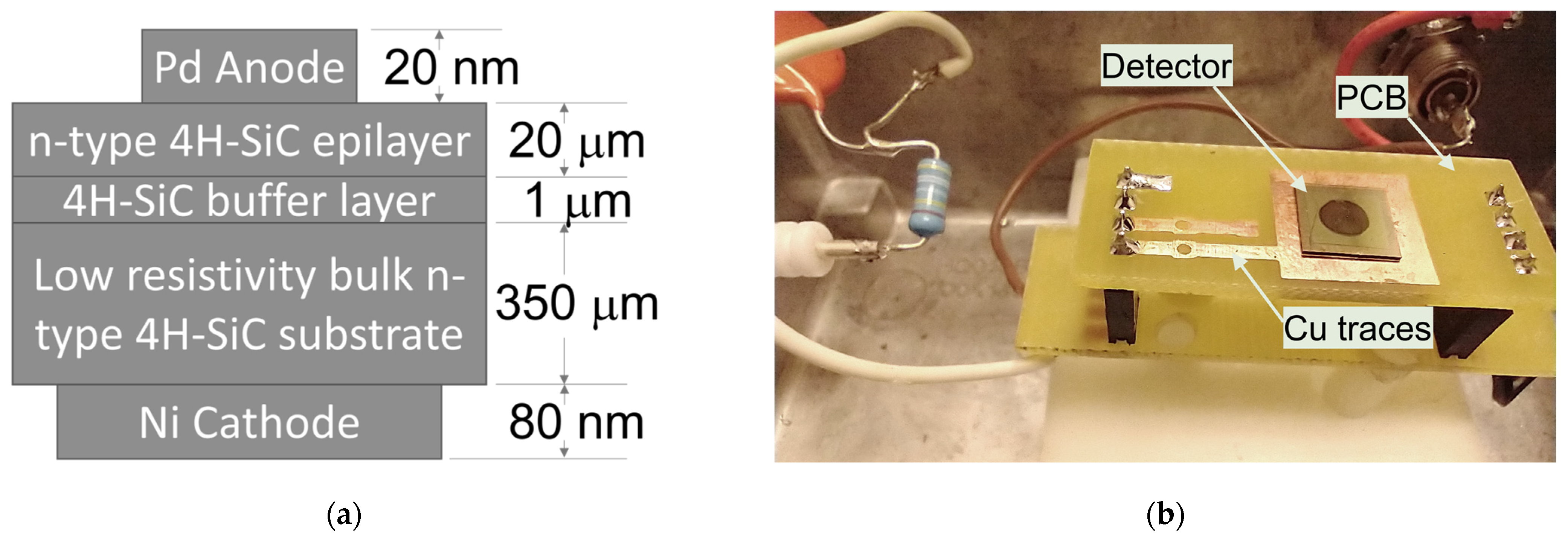
N-type 4H-SiC epilayers with an average thickness of 20 µm were grown on the (100) plane of a 100 mm diameter heavily doped n-type 4H-SiC substrate 4
off-cut towards the [11
0] crystal direction using chemical vapor deposition (CVD). The epitaxial wafer was diced into square specimens with an edge length of 8 mm followed by an RCA cleaning. Ohmic back contacts were obtained by depositing 80 nm thick square (6 mm × 6 mm) Ni using a benchtop Quorum Q150T DC sputter coater. Circular Pd contacts with thickness 20 nm and area ≈11 mm
2 were sputter coated on the epilayer side to obtain the Schottky junction. The cross-sectional view of the wafer structure and a photograph of a detector used in this study is shown in
Figure 1a,b, respectively.
The electrical characterization of the detector was carried out at room temperature under dark ambience through current-voltage and capacitance-voltage measurements using a Keithley 237 source-measure unit and a high frequency (1 MHz) Sula Technologies DDS-12 capacitance meter, respectively. The detectors were mounted on custom-made PCBs installed inside an electronic test-box shielded from electromagnetic interference (EMI). Defect levels were analyzed using a Sula Technologies DDS-12 deep level transient spectrometer (DLTS). The detectors were mounted on a Cu holder installed inside a Janis VPF-800 liquid nitrogen cooled cryostat controlled by a Lakeshore LS335 temperature controller. The DLTS system comprises a pulse generator, a 1 MHz oscillator, a correlator module, a femto-Farad resolution capacitance meter, and a preamplifier module. The DDS-12 allows fully automated DLTS scans in the temperature range 80–800 K controlled by a data acquisition program coded in LabVIEW platform. The detectors were pulsed to 0 V from a steady state reverse bias,
set at −9 V with a pulse width of 2 msec during which the depletion width collapses and fills the majority carrier (electron) trap centers. Following the pulsing, the bias returned to the steady state immediately, while the trapped electrons gradually detrapped to the conduction band. The relaxation period depended on the rate window setting and varied between 50 and 1000 msec. The DDS-12 system allows one to select twelve rate windows. The time positions of the rate windows (
) are set by initial delays
, ranging from 0.02 msec to 100 msec, measured from the end of the trap-filling pulse. The rate window and the initial delay are related as below.
The 4H-SiC detectors were mounted inside an EMI shielded test box for the pulse height spectroscopy. The test box was constantly evacuated during the measurement using a mechanical pump to maintain a vacuum of <1 × 10⁻⁴ Torr that minimizes the scattering of alpha particles with air molecules. A 0.9 μCi 241Am alpha particle source was placed 1.5 cm above the Pd window of the detector. The broad window alpha source was used to ensure uniform illumination of the whole detector window. A Cremat CR110 charge sensitive preamplifier was used to collect the detector signals and an Ortec 671 spectroscopy amplifier was used to filter and amplify the preamplifier output. A Canberra Multiport II ADC/MCA unit controlled by a Genie 2000 data acquisition program was used to acquire the pulse height spectra (PHS).
An absolute calibration method was adopted to correlate the MCA channel numbers to the energy of the detected radiation [
29]. A precision pulser generating waveforms similar to detector output signals was connected to the preamplifier input through a feedthrough capacitor with capacitance
. The amplitudes of the charge pulses (
, mV) from the capacitor were converted to energy equivalent from a 4H-SiC detector (
in keV) using Equation (2) below:
In the above equation is the ehp generation energy (7.3 eV for 4H-SiC). A set of PHS was acquired for different s by adjusting the amplitudes of the pulser output. The corresponding peak position and the energy were plotted in a graph to obtain a correlation between radiation energy and the peak position in the MCA.
The charge collection efficiency (CCE), , was calculated as the ratio of energy read by the detector () to the energy of the incident particles (~5486 keV) when the detector was illuminated by the alpha source. was derived from the corresponding alpha peak centroid in the PHS.
The detector energy resolution was calculated as the full width at half maximum (FWHM),
, of the alpha peak in the PHS. The energy resolution has also been expressed as percentage resolution
calculated as below:
3. Results
3.1. Electrical Characterization
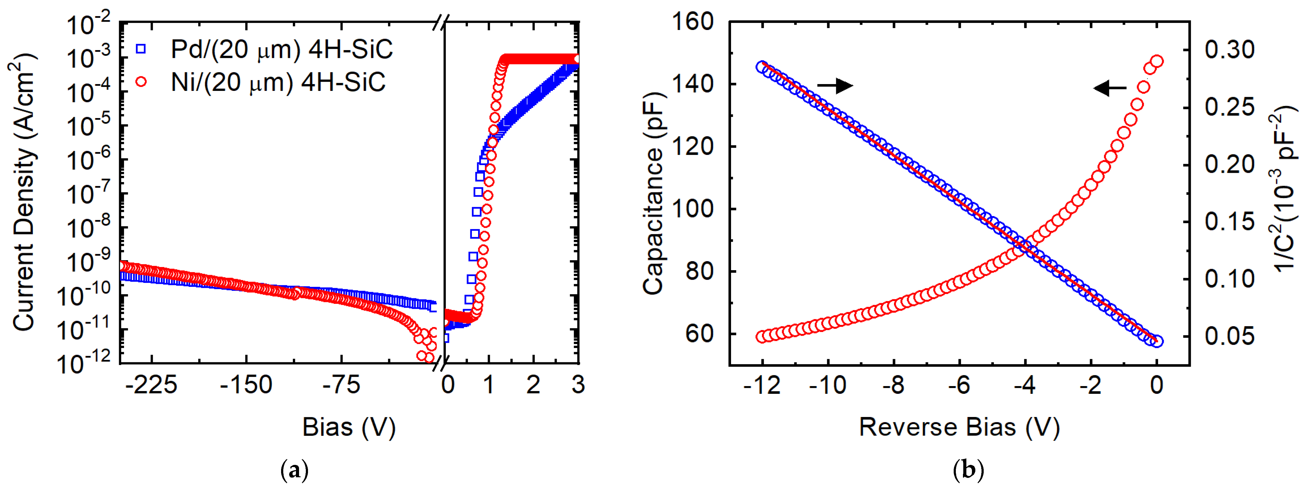
The current density-voltage (
J-V) characteristic in
Figure 2a shows the variation of leakage current density (
J) as a function of the detector bias
V. The bias has been applied to the anode (Schottky) Pd contact and measured (magnitude and polarity) with respect to the cathode (Ohmic) Ni contact kept at the ground potential. The leakage current density was calculated as the ratio of leakage current to the contact area (0.01 cm
2). A dark current density of 0.4 nA/cm
2 at −250 V was observed, which is lower than that observed in a state-of-the-art benchmark Ni/4H-SiC SBD.
Figure 2a also compares the
J-V characteristic obtained from the benchmark SBD which exhibited a leakage current density of 0.7 nA/cm
2 at −250 V. The benchmark detector is among the 4H-SiC detectors that has demonstrated record high energy resolution for 5486 keV alpha particles [
6]. Leakage current is an important device parameter as the white parallel noise increases with device leakage current affecting the energy resolution of the detector adversely [
30]. With such low leakage currents observed, the Pd/4H-SiC is poised to exhibit very high energy resolution.
The intensity of reverse leakage current in an SBD depends on the Schottky barrier height (SBH). The SBH is usually determined by fitting the experimentally obtained forward bias
J-V characteristics to a thermionic emission model given by [
31,
32],
In the above equation,
is the effective Richardson constant (146 A-cm
−2K
−2 for 4H-SiC),
is the electronic charge,
is the Boltzmann constant, and
is the absolute temperature. From the fitting, the diode ideality factor
and the SBH
were calculated to be 1.1 and 1.5 eV, respectively. An ideality factor greater than one suggests that the barrier height is not homogeneously distributed across the entire contact area and there exist regions on the surface with lower barrier heights through which a fraction of the current flows [
33]. The calculated barrier height of 1.5 eV is thus the minimum barrier height dominated by the low Schottky barrier height locations. The benchmark Ni/4H-SiC SBD showed similar junction properties with an ideality factor of 1.2 and a Schottky barrier height of 1.6 eV [
1,
4,
6].
The average barrier height for the entire diode area can be determined indirectly from the capacitance-voltage (
C-V) characteristics [
34].
Figure 2b shows the
C-V characteristics measured for the Pd/4H-SiC SBD along with the Mott–Schottky (
A2/
C2 vs.
V) plot where
A is the contact area. From the slope
of the linear fit of
A2/
C2 vs.
V plot and Equation (5) below, the effective doping concentration,
, in the detector’s active region was calculated to be 1.63 × 10
14 cm
−3.
where,
is the dielectric constant of 4H-SiC (9.66) and
is the permittivity of vacuum. A lower value of
ensures that for a given detector volume the full depletion width may be achieved for a smaller reverse bias. Considering the above-calculated
, the 20 μm thick epilayer would be depleted fully at a reverse bias as low as −60 V. The penetration depth of 5486 keV alpha particles in 4H-SiC is ≈18 μm, which ensures that, when fully depleted, all the incident alpha particles are stopped within the depletion width, a criteria required to achieve optimum charge collection efficiency and energy resolution.
The intercept of the Mott–Schottky plot on the voltage axis gives the built-in potential
Vbi, which was calculated to be 2.03 V. The
Vbi for the benchmark Ni/4H-SiC SBD has been reported to be 2.1 V. Such high built-in potential is crucial to obtaining high charge collection efficiency and energy resolution in the self-biased (0 V applied bias) mode of operation. Self-biased operation is a highly sought after property for remotely operated detectors where carrying power supplies is a challenge, such as in space missions [
35,
36]. The average barrier height calculated using Equation (6) below was found to be 2.33 eV [
37].
where,
is the potential difference between the Fermi level and the conduction band minimum in the neutral region of the semiconductor.
is expressed as
where
is the effective density of states in the conduction band of 4H-SiC and is taken to be 1.6 × 10
19 cm
−3, and
, the donor concentration, is taken to be equal to
.
3.2. Radiation Detection
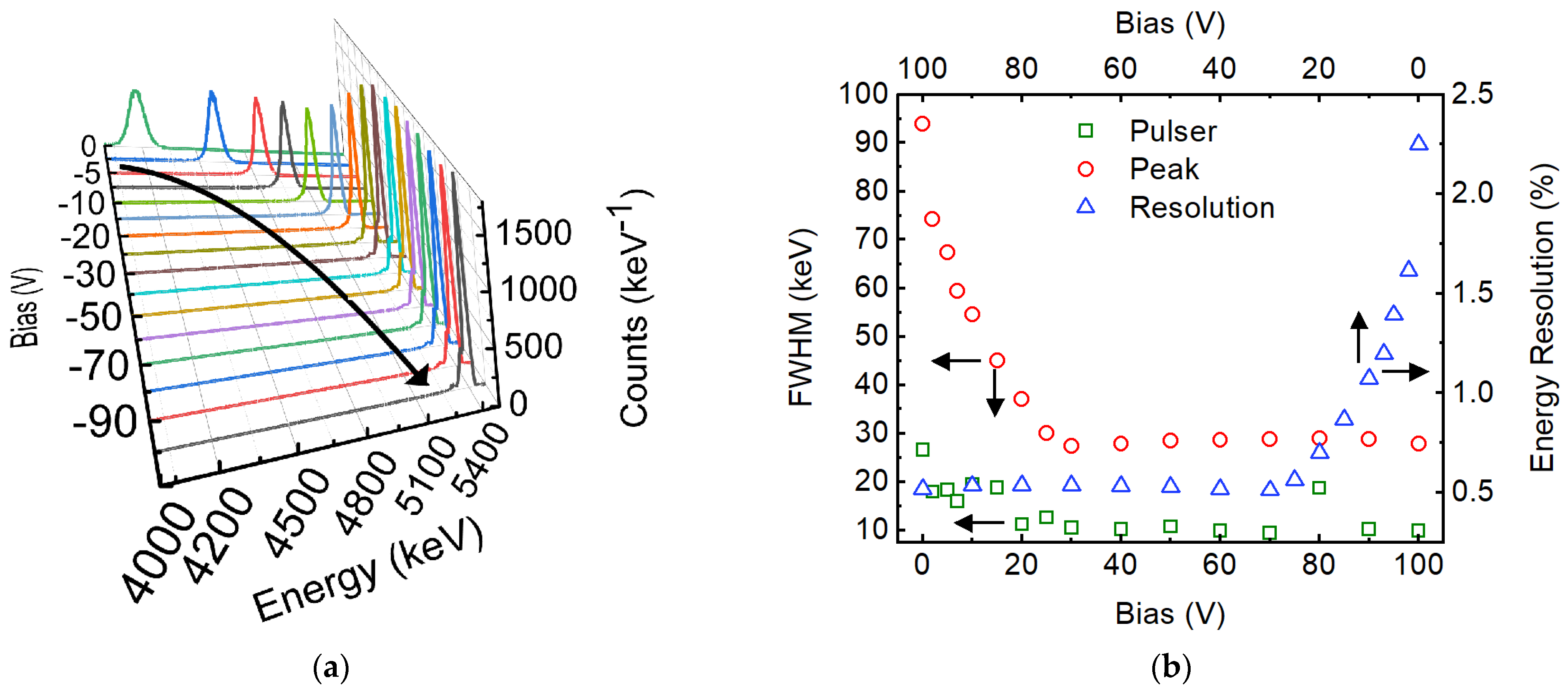
The junction properties observed in the Pd/4H-SiC SBD from the electrical measurements indicate high-resolution and high-efficient detection performance.
Figure 3a shows the pulse height spectra obtained at different bias voltages starting from 0 V to −100 V with the detector illuminated by the alpha particle source. The self-biased detector showed a robust peak corresponding to the 5486-keV alpha particles. As is evident from the increase in the height of the peak corresponding to the 5486-keV alpha particles and its shift towards the higher energy channel in
Figure 3a, the performance of the detector improved consistently with increase in reverse bias. The shift of the peak in the energy channel indicates an increase in charge collection efficiency, and the increase in peak height indicates a narrower peak (high resolution) for a given data acquisition period. The data acquisition time for each spectrum was set to 300 secs.
Figure 3b shows the variation of detector energy resolution as a function of reverse bias along with that of the pulser peak width. The pulser peak width, recorded along with the alpha PHS, is a measure of the electronic noise in the detector system, which also includes the noise due to the detector leakage current and capacitance. The percentage energy resolution has also been plotted in the same graph. The energy resolution could be seen to improve (decrease in FWHM) drastically until a reverse bias of −30 V. The improvement is primarily due to the lowering of the detector capacitance, which controls both the white series and pink noise. The lowering of the electronic noise is evident from the decrease in the pulser peak FWHM. Beyond −30 V, the change in the detector capacitance almost saturated, leading to the saturation of the detector resolution as well. The electronic noise (pulser width) was seen to be far below the detector peak width, even at the optimized detector bias.
Figure 4 shows the variation of the CCE determined experimentally (
) as a function of the reverse bias. As expected, the CCE improved with reverse bias up to −30 V due to the increase in drift velocity. At lower bias, and with the depletion width being narrow, most of the charge pairs are created beyond the depletion width i.e., in the neutral region. Since the electric field is almost absent within the neutral region, the only charges that are collected by the detector are the holes that reach the edge of the depletion width. With increasing bias, the depletion width increases, and the number of electrons created within the depletion width along the path of the alpha particles and the number of holes reaching the edge of the depletion width both increase, thereby increasing the charge collection efficiency significantly. The contribution from drift and diffusion of the charge carriers separately to the overall charge collection efficiency can be determined by fitting the variation of
as a function of the reverse bias to a drift-diffusion model, given by Equation (8) below [
38].
In the above equation,
is the depletion width at a set bias,
is the penetration depth of the incident alpha particles in 4H-SiC,
is the electronic stopping power of the alpha particles calculated using SRIM 2013 [
39], and
is the minority carrier (hole) diffusion length. It can be observed from the plot in
Figure 4 that
dominates over
until a reverse bias of −30 V, where the depletion width becomes comparable to the penetration depth of the alpha particles and the CCE is dominated by the drifting of charge carriers within the depletion width. Hence, above a reverse bias of −30 V, the
values approached the
values. From the fitting, the
was calculated to be 30.8 μm, which is much longer than the 18.6 μm calculated in the benchmark Ni/4H-SiC SBD.
As mentioned earlier, in the present detector a robust alpha peak at zero applied bias has been obtained. The CCE in the self-biased mode was calculated to be ~76%, which is very close to that reported (≈82%) for 4H-SiC detectors with the highest CCE in self-biased mode [
40]. The energy resolution of the detector in the self-biased mode was calculated to be 1.9% (81 keV) for the 5486 keV alpha particles, which is high enough for spectroscopic purposes. Such high CCE and energy resolution in the self-biased mode is due to the long hole diffusion length and the high built-in potential obtained for the Pd/4H-SiC SBD. The CCE and the energy resolution reached 98% and 0.49% (27 keV), respectively, for 5486 keV alpha particles at the optimized bias voltage of −50 V. The detailed pulse height spectra obtained in the self-biased mode and under the optimized biasing conditions are shown in
Figure 5a,b, respectively.
Table 1 summarizes the junction and the detector properties obtained for the present detectors.
3.3. Defect Characterization
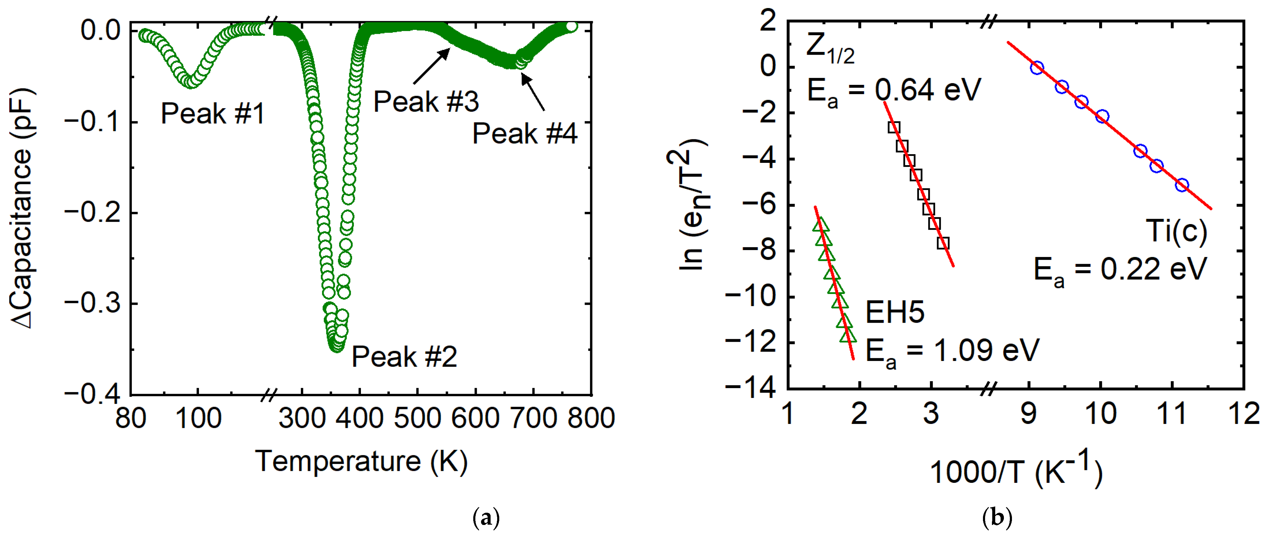
A typical DLTS spectrum obtained for the Pd/4H-SiC SBD is plotted in
Figure 6a, which shows three well-resolved and one partially resolved peaks in the temperature scan range 80–790 K. The peaks in a DLTS scan form due to the resonant emission rate of trapped electrons from a trap center at a particular rate window setting [
41]. The capacitance transients
due to the thermal emission of charge carriers from a trapping center are given by
where
is the capacitance change at time
0 due to charge trapping by the trap center indexed
,
is the background capacitance at 0 V. The emission rate
of the
th trap center is described by the Equation (10) below.
where
is the mean thermal velocity of charge carriers,
is the capture cross-section, and
is the activation energy (considering electron trap centers) calculated as the energy level of the trap center
measured relative to the conduction band minimum
. For an initial delay
and a time
after a rate window
, the DLTS signal
Si(
T) is expressed as,
From the emission rate corresponding to the peaks, the Arrhenius plots can be generated, following Equation (10), to calculate the activation energies and capture cross sections of the trap centers. The trap concentration
is calculated using Equation (12) below [
41].
Figure 6b shows the Arrhenius plots corresponding to the three fully resolved peaks observed in the DLTS spectra. The partially resolved peak could not be analyzed due to the high uncertainty in the peak position. The defect parameters calculated from the Arrhenius plots and Equation (12) have been provided in
Table 2. Peak #1 situated 0.22 eV below the conduction band minimum is well-studied and has been identified with the transition from the +3-charge state to +2 of substitutional titanium in the cubic lattice site and is labelled as Ti(c) [
42]. The Ti impurity appears from the Ti crucible used in the growth process and is known to appear in as-grown SiC [
43,
44]. Peak #2 located 0.64 eV below the conduction band minimum corresponds to the Z
1/2 center which has been identified as carbon vacancies from annealing studies using DLTS and electron paramagnetic resonance (EPR) [
16,
25,
45,
46]. Peak #4 is located at 1.09 eV below the conduction band minimum and resembles the EH5 trap center. EH5 trap center has been assigned to a carbon-related antisite–vacancy (CAV) pair in 4H-SiC [
47,
48].
4. Discussion
The energy resolution of 4H-SiC Schottky barrier detectors primarily depends on three factors: semiconductor material properties, Schottky junction properties, and the defect parameters. While the material properties such as effective doping concentration determines the junction capacitance and hence controls the white series and pink noises, junction parameters such as barrier height control the leakage current which in turn defines the white parallel noise in the spectrometer. White series, white parallel, and the pink noise are the three primary noise factors that define the overall electronic noise of a radiation spectrometer. Despite having vital device parameters such as barrier height, leakage current, built-in potential, hole diffusion length, and self-biased performance at par or even better than the Ni/4H-SiC benchmark SBD, the energy resolution of the Pd/4H-SiC SBD was found to be slightly lower when compared to the 0.29% observed for 5486 keV alpha particles using the benchmark detector. The electronic noise was observed to be much below the detector peak width at the optimized spectrometer setting, signifying that the detector performance is not limited by the electronic noise of the spectrometer. The above facts indicated that the detector performance is limited by the charge trapping in the lattice defects.
Capacitance mode deep level transient spectroscopy showed the presence of three trapping centers. While the Ti(c) centers are shallow impurity centers, the Z
1/2 centers are very strong trapping centers and have been dubbed as the “lifetime killer” defect. The EH
6/7 normally observed in our 4H-SiC epilayers has not been seen in these detectors, and instead a defect level with activation energy identical to EH5 center has been observed. Although EH5 is a deep defect level, the corresponding capture cross-section has been found to be on the order of 10
−17 cm
2, which is two orders of magnitude lower than the typical capture cross-sections of deep level defects, suggesting weak electron trapping in these defects. This further indicates that the Z
1/2 center is the defining trapping center in the Pd/4H-SiC detector as far as the effect of charge carrier trapping is concerned. The benchmark detector reports a concentration of ≈10
11 cm
−3 for the Z
1/2 center, which is one order of magnitude lower than that observed in the present detector [
22]. Hence, the observed difference in the energy resolution of the two detectors is attributed to the varied concentration of the Z
1/2 center.
In the self-biased mode, the Pd/4H-SiC SBD showed a much higher charge collection efficiency of 76% and an energy resolution of 1.9%; this is compared to the 57% charge collection efficiency and energy resolution of 4.3% observed in the benchmark Ni/4H-SiC SBD when exposed to 5486 keV alpha particles. The superior performance has been attributed to a longer hole diffusion length and a strong built-in potential.
Surface defects also play an important role in defining the detector performance by controlling the surface recombination velocity and surface leakage current. The effect of surface defects and surface currents in Schottky diodes may be greatly reduced by using surface passivation techniques and guard ring structures, respectively. The Pd/4H-SiC SBD and the benchmark detector are both fabricated under the same conditions where no surface passivation technique or guard ring structure has been used. Hence, the role of surface properties in the observed behavioral difference between the two detectors is thought to be minimal.
As a future plan, the authors intend to study the tolerance of the Pd/4H-SiC detectors in harsh environment conditions such as in high background radiation and high temperature environments. The authors also plan to study the effect of interfacial defects on the device performance and compare them to those observed in the benchmark detector.
5. Conclusions
Schottky barrier detectors have been fabricated by depositing 20 nm thick palladium metal films to assess their performance as radiation detectors. The Pd/4H-SiC SBD showed excellent rectification behavior, with a reverse current density lower than that observed in benchmark Ni/4H-SiC SBD at high operating voltages. The fabricated Pd/4H-SiC SBD showed a high barrier height of 1.5 eV and an ideality factor of 1.1. The ideality factor indicated spatial inhomogeneity in barrier height, which implies the presence of low barrier patches. Indeed, the average barrier height calculated from the C-V measurements was found to be 2.33 eV. The C-V measurements also showed a high built-in potential of 2.03 V. A high hole diffusion length of ≈30.8 μm was calculated using a drift-diffusion model applied to the alpha pulse height spectroscopy. The high built-in potential and the long hole diffusion length are sufficient to ensure spectroscopic grade radiation detection even in self-biased mode. In fact, the Pd/4H-SiC SBD showed an energy resolution of 1.9% and charge collection efficiency of 76% in self-biased mode which are superior to those reported for the benchmark detector. Despite having junction properties at par with the benchmark detector, the Pd/4H-SiC SBD showed a slightly lower energy resolution of 0.49% at optimized bias, compared to that of 0.29% reported for the benchmark detector for 5486 keV alpha particles. Capacitance mode DLTS measurements showed the presence of two deep levels and one shallow level trap center. The shallow level has been identified as the titanium impurity center whereas the deep levels have been identified as the Z1/2 center corresponding to carbon vacancies and the EH5 center corresponding to the carbon-antisite vacancy pair. The resolution of the fabricated Pd/4H-SiC SBD was found to be limited by the higher concentration of the Z1/2 center, which in the benchmark detector was found to be one order of magnitude less. It has been concluded that Pd/4H-SiC Schottky barrier detector has the potential to exhibit superior performance compared to conventional Ni/4H-SiC SBDs provided the effect of the Z1/2 centers are mitigated.
Author Contributions
Conceptualization, K.C.M. and S.K.C.; methodology, S.K.C., R.N. and K.C.M.; formal analysis, S.K.C., R.N. and K.C.M.; investigation, S.K.C., R.N. and K.C.M.; resources, K.C.M.; data curation, S.K.C. and R.N.; writing—original draft preparation, S.K.C. and K.C.M.; writing—review and editing, K.C.M.; visualization, K.C.M.; supervision, K.C.M.; project administration, K.C.M.; funding acquisition, K.C.M. All authors have read and agreed to the published version of the manuscript.
Funding
This work was supported in part by the DOE Office of Nuclear Energy’s Nuclear Energy University Program (NEUP), Grant No. DE-NE0008662 (K.C.M. PI). K.C.M acknowledges funding from the HSC Seed Grant, Prisma Health, Grant No. 10011863; Transformative Research Seed Grant Initiative Award No. 80004827; and South Carolina NASA EPSCoR Research Program, Grant No. 10011935.
Data Availability Statement
The data presented in this study are available on request from the corresponding author.
Conflicts of Interest
The authors declare no conflict of interest. The funding agencies had no role in the design of the study; in the collection, analyses, or interpretation of data; in the writing of the manuscript; or in the decision to publish the results.
References
- Mandal, K.C.; Kleppinger, J.W.; Chaudhuri, S.K. Advances in high-resolution radiation detection using 4H-SiC epitaxial layer devices. Micromachines 2020, 11, 254. [Google Scholar] [CrossRef] [PubMed]
- Puglisi, D.; Bertuccio, G. Silicon carbide microstrip radiation detectors. Micromachines 2019, 10, 835. [Google Scholar] [CrossRef]
- Lioliu, G.; Renz, A.B.; Shah, V.A.; Gammon, P.M.; Barnett, A.M. Mo/4H-SiC Schottky diodes for room temperature x-ray and g-ray spectroscopy. Nucl. Instrum. Methods Phys. Res. A 2022, 1027, 166330. [Google Scholar] [CrossRef]
- Mandal, K.C.; Chaudhuri, S.K.; Ruddy, F.H. High-resolution alpha spectrometry using 4H-SiC detectors: A review of the state-of-the-art. IEEE Trans. Nucl. Sci. 2023, 70, 823–830. [Google Scholar] [CrossRef]
- Bertuccio, G.; Caccia, S.; Nava, F.; Foti, G.; Puglisi, D.; Lanzieri, C.; Lavanga, S.; Abbondanza, G.; Crippa, D.; Preti, F. Ultra low noise epitaxial 4H-SiC X-ray detectors. Mater. Sci. Forum 2009, 615–617, 845–848. [Google Scholar] [CrossRef]
- Chaudhuri, S.K.; Zavalla, K.J.; Mandal, K.C. High resolution alpha particle detection using 4H–SiC epitaxial layers: Fabrication, characterization, and noise analysis. Nucl. Instrum. Method Phys. Res. A 2013, 728, 97–101. [Google Scholar] [CrossRef]
- Kasap, S.O.; Kabir, M.Z.; Ramaswami, K.O.; Johanson, R.E.; Curry, R.J. Charge collection efficiency in the presence of non-uniform carrier drift mobilities and lifetimes in photoconductive detectors. J. Appl. Phys. 2020, 128, 124501. [Google Scholar] [CrossRef]
- Neudeck, P.G. Silicon Carbide Electronic Devices. In Encyclopedia of Materials: Science and Technology; Elsevier: Amsterdam, The Netherlands, 2001. [Google Scholar]
- Neudeck, P.G.; Spry, D.J.; Chen, L.; Prokop, N.F.; Krasowski, M.J. Demonstration of 4H-SiC digital integrated circuits above 800 °C. IEEE Electron Device Lett. 2017, 38, 1082–1085. [Google Scholar] [CrossRef]
- Lucas, G.; Pizzagalli, L. Comparison of threshold displacement energies in β-SiC determined by classical potentials and ab initio calculations. Nucl. Instrum. Meth. Phys. Res. B 2005, 229, 359–366. [Google Scholar] [CrossRef]
- Kleppinger, J.W.; Chaudhuri, S.K.; Karadavut, O.; Nag, R.; Watson, D.L.; McGregor, D.S.; Mandal, K.C. Deep-level transient spectroscopy and radiation detection performance studies on neutron irradiated 250-μm thick 4H-SiC epitaxial layers. IEEE Trans. Nucl. Sci. 2022, 69, 1972–1978. [Google Scholar] [CrossRef]
- Neudeck, P.G.; Spry, D.J.; Krasowski, M.J.; Prokop, N.F.; Chen, L. Demonstration of 4H-SiC JFET digital ICs across 1000 °C temperature range without change to input voltages. Mater. Sci. Forum 2019, 963, 813–817. [Google Scholar] [CrossRef]
- Torrisi, L.; Foti, G.; Guiffrid, L.; Puglisi, D.; Wolowski, J.; Badziak, J.; Parys, P.; Rosinski, M.; Margarone, D.; Krasa, J.; et al. Single crystal silicon carbide detector of emitted ions and soft x rays from power laser-generated plasmas. J. Appl. Phys. 2009, 105, 123304. [Google Scholar] [CrossRef]
- Bertuccio, G.; Puglisi, D.; Torrisi, L.; Lanzieri, C. Silicon carbide detector for laser-generated plasma radiation. Appl. Surf. Sci. 2013, 272, 128–131. [Google Scholar] [CrossRef]
- Schlichting, H.; Lim, M.; Becker, T.; Kallinger, B.; Erlbacher, T. The influence of extended defects in 4H-SiC epitaxial layers on gate oxide performance and reliability. Mater. Sci. Forum 2023, 1090, 127–133. [Google Scholar] [CrossRef]
- Chaturvedi, M.; Haasmann, D.; Moghadam, H.A.; Dimitrijev, S. Electrically active defects in SiC power MOSFETs. Energies 2023, 16, 1771. [Google Scholar] [CrossRef]
- Huang, X.R.; Dudley, M.; Vetter, W.M.; Huang, W.; Si, W.; Carter, C.H., Jr. Superscrew dislocation contrast on synchrotron white-beam topographs: An accurate description of the direct dislocation image. J. Appl. Cryst. 1999, 32, 516–524. [Google Scholar] [CrossRef]
- Sumakeris, J.J.; Jenny, J.R.; Powell, A.R. Bulk crystal growth, epitaxy, and defect reduction in silicon carbide materials for microwave and power devices. MRS Bull. 2005, 30, 280–286. [Google Scholar] [CrossRef]
- Kleppinger, J.W.; Chaudhuri, S.K.; Karadavut, O.; Mandal, K.C. Defect characterization and charge transport measurements in high-resolution. Ni/n-4H SiC Schottky barrier radiation detectorsfabricated on 250 μm epitaxial layers. J. Appl. Phys. 2021, 129, 244501. [Google Scholar] [CrossRef]
- Vittone, E.; Olivero, P.; Jakšiċ, M.; Pastuović, Ž. 4H-SiC Schottky diode radiation hardness assessment by IBIC microscopy. Nucl. Instrum. Methods Phys. Res. B 2023, 537, 14–22. [Google Scholar] [CrossRef]
- Nguyen, K.V.; Mannan, M.A.; Mandal, K.C. Improved n-type 4H-SiC epitaxial radiation detectors by edge termination. IEEE Trans. Nucl. Sci. 2015, 62, 3199–3206. [Google Scholar] [CrossRef]
- Mandal, K.C.; Chaudhuri, S.K.; Nguyen, K.V.; Mannan, M.A. Correlation of deep levels with detector performance in 4H-SiC epitaxial Schottky barrier alpha detectors. IEEE Trans. Nucl. Sci. 2014, 61, 2338–2344. [Google Scholar] [CrossRef]
- Chaudhuri, S.K.; Kleppinger, J.W.; Mandal, K.C. Radiation detection using fully depleted 50 μm thick Ni/n-4H-SiC epitaxial layer Schottky diodes with ultra-low concentration of Z1/2 and EH6/7 deep defects. J. Appl. Phys. 2020, 128, 114501. [Google Scholar] [CrossRef]
- Iwamoto, N.; Johnson, B.C.; Hoshino, N.; Ito, M.; Tsuchida, H.; Kojima, K.; Ohshima, T. Defect-induced performance degradation of 4H-SiC Schottky barrier diode particle detectors. J. Appl. Phys. 2013, 113, 143714. [Google Scholar] [CrossRef]
- Danno, K.; Kimoto, T. Investigation of deep levels in n-type 4H-SiC epilayers irradiated with low-energy electrons. J. Appl. Phys. 2006, 100, 113728. [Google Scholar] [CrossRef]
- Klein, P.B.; Shanabrook, B.V.; Huh, S.W.; Polyakov, A.Y.; Skowronski, M.; Sumakeris, J.J.; O’Loughlin, M.J. Lifetime-limiting defects in n- 4H-SiC epilayers. Appl. Phys. Lett. 2006, 88, 052110. [Google Scholar] [CrossRef]
- Han, S.Y.; Shin, J.-Y.; Lee, B.-T.; Lee, J.-L. Microstructural interpretation of Ni ohmic contact on n-type 4H-SiC. J. Vac. Sci. Technol. B 2002, 20, 1496–1500. [Google Scholar] [CrossRef]
- Gora, V.E.; Auret, F.D.; Danga, H.T.; Tunhuma, S.M.; Nyamhere, C.; Igumbor, E.; Chawanda, A. Barrier height inhomogeneities on Pd/n-4H-SiC Schottky diodes in a wide temperature range. Mater. Sci. Eng. B 2019, 247, 114370. [Google Scholar] [CrossRef]
- Alruhaili, A.; Sellin, P.J.; Lohstroh, A.; Veeramani, P.; Kazemi, S.; Veale, M.C.; Sawhney, K.J.S.; Kachkanov, V. Performance characteristics of CdTe drift ring detector. J. Instrum. 2014, C03029, 2014. [Google Scholar] [CrossRef]
- Bertuccio, G.; Pullia, A. A method for the determination of the noise parameters in preamplifying systems for semiconductor radiation detectors. Rev. Sci. Instrum. 1993, 64, 3294–3298. [Google Scholar] [CrossRef]
- Rhoderick, E.H.; Williams, R.H. Metal-Semiconductor Contacts; Clarendon Press: Oxford, UK, 1988. [Google Scholar]
- Tadjer, M.J.; Hobart, K.D.; Anderson, T.J.; Feygelson, T.I.; Myers-Ward, R.L.; Koehler, A.D.; Calle, F.; Eddy, C.R.; Kurt Gaskill, D.; Pate, B.B.; et al. Thermionic-field emission barrier between nanocrystalline diamond and epitaxial 4H-SiC. IEEE Electron Device Lett. 2014, 35, 1173–1175. [Google Scholar] [CrossRef]
- Tung, R.T. The physics and chemistry of the Schottky barrier height. Appl. Phys. Rev. 2014, 1, 011304. [Google Scholar] [CrossRef]
- Knoll, G.F. Radiation Detection and Measurements; John Wiley: Hoboken, NJ, USA, 2010. [Google Scholar]
- Ha, J.H.; Kang, S.M.; Park, S.H.; Kim, H.S.; Lee, N.H.; Song, T.-Y. A self-biased neutron detector based on an SiC semiconductor for a harsh environmen. Appl. Radiat. Isot. 2009, 67, 1204–1207. [Google Scholar] [CrossRef] [PubMed]
- Chaudhuri, S.K.; Nag, R.; Mandal, K.C. Self-biased Mo/n-4H-SiC Schottky barriers as high-performance ultraviolet photodetectors. IEEE Electron Device Lett. 2023, 44, 733–736. [Google Scholar] [CrossRef]
- Jang, M.; Kim, Y.; Shin, J.; Lee, S. Characterization of erbium-silicided Schottky diode junction. IEEE Electron Device Lett. 2005, 26, 354–356. [Google Scholar] [CrossRef]
- Breese, M.B.H. A theory of ion beam induced charge collection. J. Appl. Phys. 1993, 74, 3789–3799. [Google Scholar] [CrossRef]
- Ziegler, J.F.; Ziegler, M.D.; Biersack, J.P. SRIM—The stopping and range of ions in matter (2010). Nucl. Instrum. Meth. Phys. Res. B 2010, 268, 1818–1823. [Google Scholar] [CrossRef]
- Chaudhuri, S.K.; Karadavut, O.; Kleppinger, J.W.; Nag, R.; Yang, G.; Lee, D.; Mandal, K.C. Enhanced hole transport in Ni/Y2O3/n-4H-SiC MOS for self-biased radiation detection. IEEE Electron Device Lett. 2022, 43, 1416–1419. [Google Scholar] [CrossRef]
- Lang, D.V. Deep-level transient spectroscopy: A new method to characterize traps in semiconductors. J. Appl. Phys. 1974, 45, 3023–3032. [Google Scholar] [CrossRef]
- Dalibor, T.; Pensl, G.; Nordell, N.; Schöner, A. Electrical properties of the titanium acceptor in silicon carbide. Phys. Rev. B 1997, 55, 13618–13624. [Google Scholar] [CrossRef]
- Zhang, J.; Storasta, L.; Bergman, P.J.; Son, P.J.; Janzén, J.E. Electrically active defects in n-type 4H–silicon carbide grown in a vertical hot-wall reactor. J. Appl. Phys. 2003, 93, 4708–4714. [Google Scholar] [CrossRef]
- Gelczuk, Ł.; Dąbrowska-Szata, M.; Sochacki, M.; Szmidt, J. Characterization of deep electron traps in 4H-SiC junction barrier Schottky rectifiers. Solid State Electron 2014, 94, 56–60. [Google Scholar] [CrossRef]
- Storasta, L.; Tsuchida, H.; Miyazawa, T.; Ohshima, T. Enhanced annealing of the Z1/2 defect in 4H–SiC epilayers. J. Appl. Phys. 2008, 103, 013705. [Google Scholar] [CrossRef]
- Son, N.T.; Trinh, X.T.; Løvlie, L.S.; Svensson, B.G.; Kawahara, K.; Suda, J.; Kimoto, T.; Umeda, T.; Isoya, J.; Makino, T.; et al. Negative-U system of carbon vacancy in 4H-SiC. Phys. Rev. Lett. 2012, 109, 187603. [Google Scholar] [CrossRef] [PubMed]
- Beyer, F.C.; Hemmingsson, C.G.; Pedersen, H.; Henry, A.; Isoya, J.; Morishita, N.; Ohshima, T.; Janzén, E. Capacitance transient study of a bistable deep level in e−-irradiated n-type 4H–SiC. J. Phys. D Appl. Phys. 2012, 45, 455301. [Google Scholar] [CrossRef]
- Karsthof, R.; Bathen, M.E.; Galeckas, A.; Vines, L. Conversion pathways of primary defects by annealing in proton-irradiated n-type 4H-SiC. Phys. Rev. B 2020, 102, 184111. [Google Scholar] [CrossRef]
| Disclaimer/Publisher’s Note: The statements, opinions and data contained in all publications are solely those of the individual author(s) and contributor(s) and not of MDPI and/or the editor(s). MDPI and/or the editor(s) disclaim responsibility for any injury to people or property resulting from any ideas, methods, instructions or products referred to in the content. |
© 2023 by the authors. Licensee MDPI, Basel, Switzerland. This article is an open access article distributed under the terms and conditions of the Creative Commons Attribution (CC BY) license (https://creativecommons.org/licenses/by/4.0/).


