Article

Optical Logic Gates Based on Z-Shaped Silicon Waveguides at 1.55 μm

1
GPL Photonics Laboratory, State Key Laboratory of Luminescence and Applications, Changchun Institute of Optics, Fine Mechanics and Physics, Chinese Academy of Sciences, Changchun 130033, China
2
Department of Physics, Faculty of Science, University of Fayoum, Fayoum 63514, Egypt
3
Lightwave Communications Research Group, Department of Electrical and Computer Engineering, School of Engineering, Democritus University of Thrace, 67100 Xanthi, Greece
4
Department of Aerospace Science and Technology, National Kapodistrian University of Athens, 34400 Psahna Evias, Greece
5
The Institute of Optics, University of Rochester, Rochester, NY 14627, USA
*
Authors to whom correspondence should be addressed.
Micromachines 2023, 14(6), 1266; https://doi.org/10.3390/mi14061266
Submission received: 26 May 2023 / Revised: 16 June 2023 / Accepted: 16 June 2023 / Published: 18 June 2023
(This article belongs to the Special Issue Novel Silicon-Based Optoelectronic Devices)

Abstract

:
In the last ten years, silicon photonics has made considerable strides in terms of device functionality, performance, and circuit integration for a variety of practical uses, including communication, sensing, and information processing. In this work, we theoretically demonstrate a complete family of all-optical logic gates (AOLGs), including XOR, AND, OR, NOT, NOR, NAND, and XNOR, through finite-difference-time-domain simulations using compact silicon-on-silica optical waveguides that operate at 1.55 μm. Three slots, grouped in the shape of the letter Z, make up the suggested waveguide. The function of the target logic gates is based on constructive and destructive interferences that result from the phase difference experienced by the launched input optical beams. These gates are evaluated against the contrast ratio (CR) by investigating the impact of key operating parameters on this metric. The obtained results indicate that the proposed waveguide can realize AOLGs at a higher speed of 120 Gb/s with better CRs compared to other reported designs. This suggests that AOLGs could be realized in an affordable manner and with improved outcomes to enable the satisfaction of the current and future requirements of lightwave circuits and systems that critically rely on AOLGs as core building elements.

1. Introduction

By merely expanding the quantity of discrete optical channels, the extreme complexity of next-generation high-capacity data transmission systems cannot be solved. The integration density of optoelectronic devices can be greatly increased while keeping cost and energy consumption low owing to silicon photonics. The silicon-on-insulator (SOI) platform, a production method in which a thin silicon layer is placed on top of an insulator substrate formed of silica (i.e., SiO2), uses silicon as its primary raw material. Due to waveguiding silicon’s high refractive index (nsilicon = 3.48) in comparison to air (nair = 1) or the silica cladding layer (nsilica = 1.44), the strong optical guiding is ensured for all signals around the typical near-infrared wavelength of 1.55 μm. There are many excellent reasons why the SOI platform has evolved into silicon photonics. For instance, silicon is broadly accessible and compatible with advanced CMOS technology, making it possible to produce structures with sizes as small as 10 nm at a reasonable price [1,2,3,4,5,6]. Due to silicon’s strong optical confinement, which allows for bending waveguide radii of only a few micrometers and functional waveguide elements of just ten to a few hundred micrometers, incredibly compact optical devices can be created [7]. In contrast, all-optical logic gates (AOLGs) overcome the disadvantages of their electronic counterparts, namely the low bandwidth and slow data transit speed, thus enabling more effective data processing. AOLGs have recently been realized using a variety of waveguide configurations [8,9,10,11,12,13,14,15,16,17,18,19,20,21,22,23,24,25,26,27,28,29]. In contrast to the basic waveguide suggested in this research, which can execute seven logic gates concurrently, the majority of these earlier designs have utilized photonic crystals (PCs) to execute only one or, at most, two logic gates [9,10,11,12,13,14,15,16,17]. Additionally, as opposed to silicon and silica that are proposed to be employed in the present design, other documented initiatives have utilized more affordable noble metals [23,24,25,26,27]. In line with earlier efforts [8,9,10,11,12,13,14,15,16,17,18,19,20,21,22,23,24,25,26,27,28,29], in this paper, we simulate a full family of AOLGs, including XOR, AND, OR, NOT, NOR, NAND, and XNOR, using Z-shaped silicon-on-silica waveguides at 1.55 μm telecommunications wavelength. Three slots that are arranged to form the letter Z make up the proposed waveguide. Based on the idea of constructive interference (CI) and destructive interference (DI) brought on by the phase discrepancies experienced by the launched input optical beams, these logic gates operate. In the FDTD simulations carried out in the commercially available Lumerical software [30], to evaluate and show the behavior of the suggested logic gates, a convolutional completely matched layer is employed as an absorbing boundary condition [22]. The performance of the proposed operations is evaluated against the contrast ratio (CR) metric. The simulation results reveal that owing to the devised waveguide-based structure, the target AOLGs can be executed with improved performance at a faster rate than other design counterparts described in the literature [8,12,13,14,19,22,24,25,26,27], which is technologically feasible. To this end, these AOLGs can serve as the key modules in fundamental- and system-oriented-level modern applications.

2. Waveguide Structure

The proposed waveguide, which has a silicon core and a silica substrate as the cladding, has three identical slots organized in the shape of the letter Z. The Z-shaped silicon waveguide is illustrated schematically in Figure 1, together with the 3D FDTD view and the corresponding field intensity distributions.
The three input ports of the waveguide are excited by a transverse magnetic mode polarized electromagnetic pulse at 1.55 μm. The simulation results are recorded by the FDTD monitors. The output spectral transmission (T) is   T = I out / I in , where Iout is the intensity at the output port (Pout) and Iin = I1 + I2 + I3 is the sum of the intensities at three input ports [22,27]. The normalized threshold transmission (Tth), which denotes the minimal normalized power necessary to produce T, is initially chosen to have a value of 0.12. When T > Tth, Pout produces ‘1’, while when T < Tth, Pout produces a ‘0’. To optimize T, the input beams must meet specific phase-matching conditions [31,32]. DI scatters the beams when the waveguide’s and input beams’ phases are out of phase, producing an output of ‘0’. A crucial statistic for describing logic functions is the CR, which is defined as CR dB = 10   ln P mean 1 / P mean 0 , where   P mean 1   and P mean 0 are the mean peak powers of logic ‘1’ and ‘0’, respectively [22]. Table 1 contains the default simulation parameters. To obtain a higher CR, the FDTD simulations have been iteratively run to optimize these parameters.

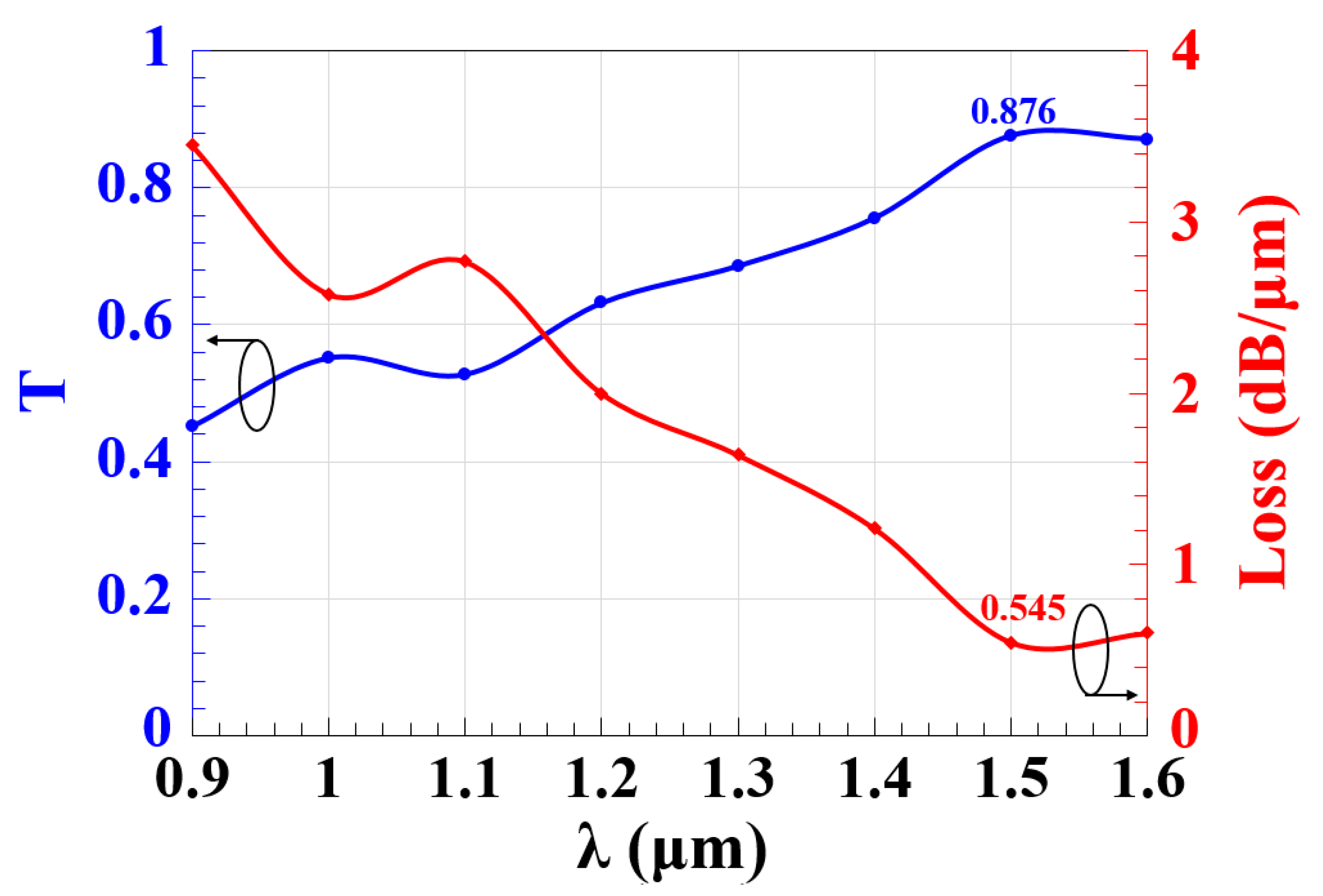
3. Waveguide Performance

Figure 2 illustrates T and the loss of the Z-shaped silicon waveguide as functions of λ, presuming that all incident beams are launched at the three input ports with an equal phase of 180°. Using the proposed waveguide, a high T of 0.876 and a low loss of 0.575 dB/μm are attained at 1.55 μm. These insignificant propagation losses are caused by scattering at the slots’ edges and material absorption. By elaborating more on this figure, it becomes clear that this waveguide operates with high T and low loss over 1.3–1.6 μm.
The performance of the suggested waveguide is crucially influenced by the angle between slots (i.e., θ). As a consequence, using the suggested Z-shaped silicon waveguide, Figure 3 simulates the effect of this parameter on T at 1.55 μm. The highest T of 0.876 occurs at θ = 70°, making the latter the best value to use throughout simulations. By expanding on this figure, it can also be seen that by changing the value of θ, the amount of light scattering and absorption inside the materials is increased, which raises losses.
The waveguide performance is significantly influenced by the shape of its arms. Therefore, T as a function of the length of the short slot (L1) and the length of the long slot (L2) at 1.55 μm is depicted in Figure 4. This figure demonstrates that the proposed Z-shaped silicon waveguide produces high T over the whole ranges of L1 and L2, i.e., L1 = 0.8–1.5 μm and L2 = 1.0–1.6 μm. This implies that the suggested design is practicable, especially in light of the accessibility of 3D femtosecond laser direct writing technology [33,34,35,36,37,38] and lithographical fabrication techniques [23,39,40,41].
We examined the waveguide performance on the slot width (w) at 1.55 μm to obtain more accurate findings, as shown in Figure 5. It is clear from this figure that the Z-shaped silicon waveguide achieves high T for a wide range of w, i.e., 0.2–0.5 μm. With the advancement of nanofabrication techniques, this finding also shows that this design might be put to use and turned into a functional prototype [23,33,34,35,36,37,38,39,40,41].
The Nyquist formula, which is defined as   2 B log 2 M , where M is the total number of signal levels and B is the optical bandwidth, determines the speed of a transmission system [42]. In this formula, B = ( c / λ 2 ) Δ λ , where c is the light speed in a vacuum, λ = 1.55 μm is the optical carrier wavelength, and Δλ is the signal spectral width [22]. This indicates that for our case, where B = 30 GHz and M = 4 (i.e., 00, 01, 10, and 11), the employed waveguide operates at a high speed of 120 Gb/s.

4. XOR, AND, OR

The XOR, AND, and OR logic gates are implemented by injecting a clock beam (Clk) into Pin1, while the other two input beams are fed into Pin2 and Pin3 (see Figure 1). The Clk (all ‘1’s) is required to induce interference, which can be either constructive or destructive by establishing a reference phase difference between the input beams. CI happens when all input beams are launched at the same phase (i.e., ΦClk = Φ2 = Φ3 = 180°) where the input beams interact in such a way that they are aligned, leading to a ‘1’ output. In contrast, DI occurs when these beams are launched at various phases (i.e., ΦClk = 180°, Φ2 = 0°, and Φ3 = 90°) and cancel each other out, leading to a ‘0’ output.

4.1. XOR

Pout produces ‘1’ (i.e., T > Tth) as a result of the CI between the input beams when the (01, 10) combination of the latter is injected along with the Clk at the same phase (i.e., ΦClk = Φ2 = Φ3 = 180°). The DI between the incident beams causes ‘0’ output to occur at Pout (i.e., T < Tth) when the combination (11), along with the Clk at various phases (i.e., ΦClk = 180°, Φ2 = 0°, and Φ3 = 90°), is launched. In this manner, the XOR logic gate is formed. Figure 6 depicts the field intensity distributions of the XOR gate propagating through the Z-shaped silicon waveguide at 1.55 μm.
Our waveguide can attain a high CR = 29 dB at 1.55 μm due to the relative difference between P mean 1   and P mean 0 .  Table 2 provides an overview of the XOR simulation outcomes.

4.2. AND

When all incident beams enter the suggested waveguide at the same phase (i.e., ΦClk = Φ2 = Φ3 = 180°), Pout yields ‘1’ as a result of CI. When these incident beams are injected at a different phase, Pout emits ‘0’. In this way, the output is ‘1’ only when all inputs are ‘1’, which corresponds to the AND gate, as seen in Figure 7.
Our waveguide results in a significant CR = 33.26 dB at 1.55 μm. Table 3 lists the rest of the outcomes of the AND simulation.

4.3. OR

When the Clk is entered with the combination of input beams (01, 10, or 11) at the same phase of 180°, the result of Pout is ‘1’. The OR is thus realized as shown in Figure 8.
The OR outcomes at 1.55 μm are displayed in Table 4 in terms of T and CR. A high CR = 31.51 dB is achieved because of the significant disparity between P mean 1   and P mean 0 .
The XOR, AND, and OR gates depend on the Clk beam to operate properly. Therefore, we evaluate how well each of these three operations performs at 1.55 μm in the presence of the Clk (i.e., meaning Pin1 has ‘1’ input) and in the absence of the Clk (i.e., meaning Pin1 has ‘0’ input) using the suggested waveguide. Table 5 shows that using the Clk in the waveguide-based scheme results in much higher CRs than without using it.

5. NOT, NOR, NAND, XNOR

To execute the inverted logic gates, a Clk with an angle of 0° must be sent from Pin3 of Figure 1.

5.1. NOT

One beam is inserted into Pin1 at a different phase of 180° to implement the NOT gate. When Pin1 is set to ‘1’, Pout generates a logical ‘0’ (i.e., T < Tth) due to the DI that happens as a result of the input beams’ various phase conditions. When Pin1 is set to ‘0’, the Clk (all ‘1’s) does not undergo a differential phase and generates instead a logical ‘1’ (i.e., T > Tth) at Pout. This results in the implementation of the NOT gate, as displayed in Figure 9.
P mean 1   and P mean 0 have a significant discrepancy, which results in a high CR of 31.76 dB. Table 6 lists the NOT outcomes utilizing the suggested waveguide at 1.55 μm.

5.2. NOR

Two beams are injected into Pin1 and Pin2 of Figure 1 to carry out the NOR (NOT-OR) operation. When (01, 10, or 11) are combined and injected at different angles, DI results in a logical ‘0’ at Pout. If (00) is launched, the Clk with ΦClk = 0° will negate the phase balance of the three ports, resulting in ‘1’ at Pout. This leads to the realization of the NOR function, as seen in Figure 10.
Our waveguide achieves a high CR = 31.50 dB for the NOR gate, as shown in Table 7.

5.3. NAND

The NAND (NOT-AND) gate can be realized by injecting the Clk into Pin3 and the other two beams into Pin1 and Pin2 so that the output is ‘0’ if and only if all inputs are ‘1’. When Pin1 and Pin2 are both “OFF” (i.e., 00), the Clk having a ΦClk = 0° causes the output to become ‘1’. CI simply occurs when the Clk and (01, 10) are launched at the same angle of 0°, resulting in a ‘1’ output. The concomitant DI causes a ‘0’ output when the logic combination (11) is launched with the Clk at Φ1 = 90°, Φ2 = 180°, and ΦClk = 0° as shown in Figure 11.
P mean 1 is higher than   P mean 0 , thus leading to a high CR = 29.83 dB. The numerical outcomes of the NAND are cited in Table 8.

5.4. XNOR

The Clk enters Pin3 to build the XNOR (exclusive-XOR) gate, similar to NOR and NAND gates, while the other two beams are injected from Pin1 and Pin2. When the input beams are combined (11) and the Clk is inserted at 0°, Pout emits a ‘1’ as a result of CI. When (01) or (10) is launched with a different phase, on the other hand, Pout generates a ‘0’, as depicted in Figure 12.
The XNOR has a high CR of 31.33 dB due to the huge discrepancy between P mean 1   and P mean 0 . Table 9 lists the XNOR outcomes.

6. Comparison

Table 10 compares the ability of the suggested waveguide to realize AOLGs to those reported in the literature and used for the same purpose in terms of the building platform, operating wavelength, and achieved CR. The data shown in this table provide evidence that our waveguide is able to carry out the required logic operations with considerably greater performance in a way that is both technically and commercially feasible.
The limitations on manufacturing are frequently referred to as a bottleneck. Nanophotonics devices are used in more applications, which makes the photonic design more difficult and complex. Instead of using conventional photonic design procedures to address this issue, designers are increasingly turning to cutting-edge optimization techniques [43,44,45,46]. In contrast to the traditional methods, which involve changing relatively simple known geometries with a limited number of parameters, these new methodologies evaluate devices with totally arbitrary geometries. Devices have been developed with extraordinarily small footprints, excellent efficiency, and novel characteristics that cannot be achieved using conventional methods in order to make use of the additional degrees of freedom [47,48,49,50,51,52,53,54,55]. Silicon and silica, which are abundant in the earth’s crust and significant elements of the earth’s mantle, make up the proposed waveguide. Due to the availability of 3D FLDW technology [33,34,35,36,37,38] and lithographic manufacturing processes [23,39,40,41], it is, therefore, possible to anticipate the experimental verification of the proposed waveguide based on the major findings of this simulation. Instead of being an essential barrier, this is a technological matter issue that can be solved in practice. Additionally, the experimental implementation of multiple AOLGs based on various optical waveguides has been reported in recent years [19,23,24,56,57], paving the way to similar implementations.

7. Conclusions

Using appropriately driven Z-shaped silicon-on-silica waveguides, a set of basic logic gates were simulated at 1.55 μm. These logic gates operate according to CI and DI, which manifests as a result of the phase difference experienced by the launched input optical beams. FDTD solutions in Lumerical, the commercially available software, were used to simulate the target logic gates. The CR metric was employed to evaluate how well these logic gates perform. The impact of key operating parameters on the waveguide performance was investigated and assessed. The simulation results have demonstrated that the proposed waveguide can achieve higher CRs and speed compared to other reported designs. The proposed single AOLGs hold the promise of being connected and combined to form more sophisticated digital circuits of enhanced functionality and multistage information processing architectures. This estimate is based both on their principle of operation and technological feasibility. To this end, issues such as fan-in/fan-out capability, power consumption, tolerable attenuation, fabrication platform, building complexity, and overall practicality should be taken into account in order to identify possible trade-offs and derive specific design rules that will render this possible in a performance- and cost-efficient manner.

Author Contributions

Conceptualization, A.K.; data curation, A.K.; formal analysis, A.K.; funding acquisition, A.H.; investigation, A.K.; methodology, A.K. and K.E.Z.; project administration, A.K.; resources, A.K.; software, A.K.; supervision, C.G.; writing—original draft, A.K.; writing—review and editing, A.K. and K.E.Z. All authors have read and agreed to the published version of the manuscript.

Funding

This research received no external funding.

Data Availability Statement

Not applicable.

Acknowledgments

Amer Kotb gratefully acknowledges the President’s International Fellowship Initiative of the Chinese Academy of Sciences (Grant No. 2022VMB0013) for supporting this research.

Conflicts of Interest

The authors declare no conflict of interest.

References

  1. Lipson, M. Guiding, modulating, and emitting light on silicon—Challenges and opportunities. J. Light. Technol. 2005, 23, 4222–4238. [Google Scholar] [CrossRef]
  2. Vlasov, Y.A. Silicon photonics for next-generation computing systems. In Proceedings of the 34th European Conference on Optical Communication (ECOC 2008), Brussels, Belgium, 21–25 September 2008. paper Tu.1.A.1. [Google Scholar]
  3. Lee, B.G.; Bergmann, K. Silicon nano-photonic interconnection networks in multicore processor systems. In Proceedings of the Frontiers in Optics OSA Annual Meeting, Rochester, NY, USA, 19–23 October 2008. paper FTh S1. [Google Scholar]
  4. Thourhout, D.V.; Campenhout, J.V.; Baets, R.; Rojo-Romeo, P.; Regreny, P.; Seassal, C.; Binetti, P.; Leijtens, X.J.M.; Ntzel, R.; Smit, M.K.; et al. Photonic interconnect layer on CMOS. In Proceedings of the 33rd European Conference and Exhibition on Optical Communication (ECOC 2007), Berlin, Germany, 16–20 September 2007. paper 6.3.1. [Google Scholar]
  5. Tsybeskov, L.; Lockwood, D.J.; Ichikawa, M. Silicon photonics: CMOS going optical. Proc. IEEE 2009, 97, 1161–1165. [Google Scholar] [CrossRef]
  6. Shi, Y.; Zhang, Y.; Wan, Y.; Yu, Y.; Zhang, Y.; Hu, X.; Xiao, X.; Xu, H.; Zhang, L.; Pan, B. Silicon photonics for high-capacity data communications. Photon. Res. 2022, 10, A106–A134. [Google Scholar] [CrossRef]
  7. Tsuchizawa, T.; Yamada, K.; Fukuda, H.; Watanabe, T.; Takahashi, J.; Takahashi, M.; Shoji, T.; Tamechika, E.; Itabashi, S.; Morita, H.; et al. Microphotonics devices based on silicon microfabrication technology. IEEE J. Sel. Top. Quant. Electron. 2005, 11, 232–240. [Google Scholar] [CrossRef]
  8. Rani, P.; Kalra, Y.; Sinha, R.K. Design of all optical logic gates in photonic crystal waveguides. Optik 2015, 126, 950–955. [Google Scholar] [CrossRef]
  9. Husko, C.; Vo, T.D.; Corcoran, B.; Li, J.; Krauss, T.; Eggleton, B. Ultracompact all-optical XOR logic gate in a slow-light silicon photonic crystal waveguide. Opt. Express 2011, 19, 20681–20690. [Google Scholar] [CrossRef] [PubMed] [Green Version]
  10. Andalib, P.; Granpayeh, N. All-optical ultracompact photonic crystal AND gate based on nonlinear ring resonators. J. Opt. Soc. Am. B 2009, 26, 10–16. [Google Scholar] [CrossRef]
  11. Jandieri, V.; Khomeriki, R.; Erni, D. Realization of true all-optical AND logic gate based on the nonlinear coupled air-hole type photonic crystal waveguide. Opt. Express 2018, 26, 19845–19853. [Google Scholar] [CrossRef] [Green Version]
  12. Priya, N.H.; Swarnakar, S.; Krishna, S.V.; Kumar, S. Design and analysis of an optical three-input AND gate using a photonic crystal fiber. Appl. Opt. 2022, 61, 77–83. [Google Scholar]
  13. Priya, N.H.; Swarnakar, S.; Krishna, S.V.; Kumar, S. Design and analysis of a photonic crystal-based all-optical 3-input OR gate for high-speed optical processing. Opt. Quantum Electron. 2021, 53, 720. [Google Scholar] [CrossRef]
  14. Rao, D.G.S.; Swarnakar, S.; Palacharla, V.; Raju, K.S.R.; Kumar, S. Design of all-optical AND, OR, and XOR logic gates using photonic crystals for switching applications. Photonic Netw. Commun. 2021, 41, 109–118. [Google Scholar] [CrossRef]
  15. Swarnakar, S.; Palacharla, V.; Muduli, A.; Kumar, S. Design and optimization of photonic crystal based all-optical logic gate with enhanced contrast ratio. Opt. Quantum Electron. 2023, 55, 623. [Google Scholar] [CrossRef]
  16. Rachana, M.; Swarnakar, S.; Babu, M.R.; Swetha, P.M.; Rangaiah, Y.P.; Krishna, S.V.; Kumar, S. Optimization of an all-optical 3-input universal logic gate with an enhanced contrast ratio by exploiting T-shaped photonic crystal waveguide. App. Opt. 2022, 61, 8162–8171. [Google Scholar] [CrossRef]
  17. Swarnakar, S.; Anguluri, S.P.K.; Alluru Sreevani, A.; Kumar, S. A novel structure of all-optical optimised NAND, NOR and XNOR logic gates employing a Y-shaped plasmonic waveguide for better performance and high-speed computations. Opt. Quantum Electron. 2022, 54, 530. [Google Scholar] [CrossRef]
  18. Ishizaka, Y.; Kawaguchi, Y.; Saitoh, K.; Koshiba, M. Design of ultracompact all-optical XOR and AND logic gates with low power consumption. Opt. Commun. 2011, 284, 3528–3533. [Google Scholar] [CrossRef]
  19. Kita, S.; Nozaki, K.; Takata, K.; Shinya, A.; Notomi, M. Ultrashort low-loss Ψ gates for linear optical logic on Si photonics platform. Commun. Phys. 2020, 3, 33. [Google Scholar] [CrossRef] [Green Version]
  20. Zeng, S.; Zhang, Y.; Pun, E. Ultrasmall optical logic gates based on silicon periodic dielectric waveguides. Photon. Nanostr. Fundam. Appl. 2010, 8, 32. [Google Scholar] [CrossRef]
  21. Cui, L.; Yu, L. Multifunctional logic gates based on silicon hybrid plasmonic waveguides. Mod. Phys. Lett. B 2018, 32, 1850008. [Google Scholar] [CrossRef]
  22. Kotb, A.; Zoiros, K.E.; Li, W. Silicon-on-silica waveguides-based all-optical logic gates at 1.55 μm. Phys. Scr. 2023, 98, 035517. [Google Scholar] [CrossRef]
  23. Gao, L.; Chen, L.; Wei, H.; Xu, H. Lithographically fabricated gold nanowire waveguides for plasmonic routers and logic gates. Nanoscale 2018, 10, 14771. [Google Scholar] [CrossRef] [Green Version]
  24. Pan, D.; Wei, H.; Xu, H. Optical interferometric logic gates based on metal slot waveguide network realizing whole fundamental logic operations. Opt. Express 2013, 21, 9556. [Google Scholar] [CrossRef] [Green Version]
  25. Bian, Y.; Gong, Q. Compact all-optical interferometric logic gates based on one-dimensional metal-insulator-metal structures. Opt. Commun. 2014, 313, 27–35. [Google Scholar] [CrossRef]
  26. Al-Musawi, H.K.; Al-Janabi, A.K.; Al-Abassi, S.A.W.; Abusiba, N.A.A.; Al-Fatlawi, N.A.Q. Plasmonic logic gates based on dielectric-metal-dielectric design with two optical communication bands. Optik 2020, 223, 165416. [Google Scholar] [CrossRef]
  27. Yao, C.; Kotb, A.; Wang, B.; Singh, S.; Guo, C. All-optical logic gates using dielectric-loaded waveguides with quasi-rhombus metasurfaces. Opt. Lett. 2020, 45, 3769–3772. [Google Scholar] [CrossRef]
  28. Keshtkar, P.; Miri, M.; Yasrebi, N. Low power, high speed, all-optical logic gates based on optical bistability in graphene-containing compact microdisk resonators. Appl. Opt. 2021, 60, 7234–7242. [Google Scholar] [CrossRef]
  29. Kotb, A.; Guo, C. 100 Gb/s all-optical multifunctional AND, XOR, NOR, OR, XNOR, and NAND logic gates in a single compact scheme based on semiconductor optical amplifiers. Opt. Laser Technol. 2021, 137, 106828. [Google Scholar] [CrossRef]
  30. Available online: www.lumerical.com/tcadproducts/fdtd/ (accessed on 31 December 2018).
  31. Smith, B.J.; Kundys, D.; Thomas-Peter, N.; Smith, P.G.R.; Walmsley, I.A. Phase-controlled integrated photonic quantum circuits. Opt. Express 2009, 17, 13516–13525. [Google Scholar] [CrossRef] [PubMed]
  32. Wang, Y.; Tian, Z.; Li, Y.; Zhang, Z.; Wang, L.; Chen, Q. Phase customization in photonic integrated circuits with trimmed waveguides. Opt. Lett. 2022, 47, 5889–5892. [Google Scholar] [CrossRef] [PubMed]
  33. Li, M.; Li, C.; Chen, Y.; Feng, L.; Yan, L.; Zhang, Q.; Bao, J.; Liu, B.; Ren, X.; Jianwei Wang, J.; et al. On-chip path encoded photonic quantum Toffoli gate. Photon. Res. 2022, 10, 1533–1542. [Google Scholar] [CrossRef]
  34. Klauck, F.; Heinrich, M.; Szameit, A. Photonic two-particle quantum walks in Su–Schrieffer–Heeger lattices. Photon. Res. 2021, 9, A1–A7. [Google Scholar] [CrossRef]
  35. Zhang, Q.; Li, M.; Xu, J.; Lin, Z.; Yu, H.; Wang, M.; Fang, Z.; Cheng, Y.; Gong, Q.; Li, Y. Reconfigurable directional coupler in lithium niobate crystal fabricated by three-dimensional femtosecond laser focal field engineering. Photon. Res. 2019, 7, 503–507. [Google Scholar] [CrossRef]
  36. Anton, C.; Loredo, J.C.; Coppola, G.; Ollivier, H.; Viggianiello, N.; Harouri, A.; Somaschi, N.; Crespi, A.; Sagnes, I.; Lemaitre, A.; et al. Interfacing scalable photonic platforms: Solid-state based multi-photon interference in a reconfigurable glass chip. Optica 2019, 6, 1471–1477. [Google Scholar] [CrossRef] [Green Version]
  37. Atzeni, S.; Rab, A.S.; Corrielli, G.; Polino, E.; Valeri, M.; Mataloni, P.; Spagnolo, N.; Crespi, A.; Sciarrino, F.; Osellame, R. Integrated sources of entangled photons at the telecom wavelength in femtosecond-laser-written circuits. Optica 2018, 5, 311–314. [Google Scholar] [CrossRef] [Green Version]
  38. Wei, D.; Wang, C.; Wang, H.; Hu, X.; Wei, D.; Fang, X.; Zhang, Y.; Wu, D.; Hu, Y.; Li, J.; et al. Experimental demonstration of a three-dimensional lithium niobate nonlinear photonic crystal. Nat. Photon. 2018, 12, 596–600. [Google Scholar] [CrossRef]
  39. Rizzo, A.; Dave, U.; Novick, A.; Freitas, A.; Roberts, S.P.; James, A.; Lipson, M.; Bergman, K. Fabrication-robust silicon photonic devices in standard sub-micron silicon-on-insulator processes. Opt. Lett. 2023, 48, 215–218. [Google Scholar] [CrossRef]
  40. Marshall, G.D.; Politi, A.; Matthews, J.C.F.; Dekker, P.; Ams, M.; Withford, M.J.; O’Brien, J.L. Laser written waveguide photonic quantum circuits. Opt. Express 2009, 17, 12546–12554. [Google Scholar] [CrossRef]
  41. Xu, Q.; Lipson, M. All-optical logic based on silicon micro-ring resonators. Opt. Express 2007, 15, 924–929. [Google Scholar] [CrossRef]
  42. Crisp, J.; Elliott, B. Introduction to Fiber Optics, 3rd ed.; Elsevier: Amsterdam, The Netherlands, 2005. [Google Scholar]
  43. Vercruysse, D.; Sapra, N.V.; Su, L.; Trivedi, R.; Vučković, J. Analytical level set fabrication constraints for inverse design. Sci. Rep. 2019, 9, 8999. [Google Scholar] [CrossRef] [Green Version]
  44. Molesky, S.; Lin, Z.; Piggott, A.Y.; Jin, W.; Vucković, J.; Rodriguez, A.W. Outlook for inverse design in nanophotonics. Nat. Photon. 2018, 12, 659–670. [Google Scholar] [CrossRef] [Green Version]
  45. Lu, J.; Vuckovic, J. Nanophotonic Computational Design. Opt. Express 2013, 21, 7748–7759. [Google Scholar] [CrossRef]
  46. Jensen, J.S.; Sigmund, O. Topology optimization for nano-photonics. Laser Photon. Rev. 2011, 5, 308–321. [Google Scholar] [CrossRef]
  47. Shen, B.; Wang, P.; Polson, R.; Menon, R. Integrated metamaterials for efficient and compact free-space-to-waveguide coupling. Opt. Express 2014, 22, 27175–27182. [Google Scholar] [CrossRef] [PubMed]
  48. Piggott, A.Y.; Lu, J.; Lagoudakis, K.G.; Petykiewicz, J.; Babinec, T.M.; Vučković, J. Inverse design and demonstration of a compact and broadband on-chip wavelength demultiplexer. Nat. Photon. 2015, 9, 374–377. [Google Scholar] [CrossRef] [Green Version]
  49. Shen, B.; Wang, P.; Polson, R.; Menon, R. An integrated-nanophotonics polarization beam splitter with 2.4 × 2.4 μm2 footprint. Nat. Photon. 2015, 9, 378–382. [Google Scholar] [CrossRef]
  50. Sell, D.; Yang, J.; Doshay, S.; Yang, R.; Fan, J.A. Large-Angle, Multifunctional Metagratings Based on Freeform Multimode Geometries. Nano Lett. 2017, 17, 3752–3757. [Google Scholar] [CrossRef] [PubMed]
  51. Yu, Z.; Cui, H.; Sun, X. Genetically optimized on-chip wideband ultracompact refectors and Fabry–Perot cavities. Photon. Res. 2017, 5, B15–B19. [Google Scholar] [CrossRef]
  52. Su, L.; Piggott, A.Y.; Sapra, N.V.; Petykiewicz, J.; Vučković, J. Inverse Design and Demonstration of a Compact on-Chip Narrowband Tree-Channel Wavelength Demultiplexer. ACS Photon. 2018, 5, 301–305. [Google Scholar] [CrossRef] [Green Version]
  53. Sitawarin, C.; Jin, W.; Lin, Z.; Rodriguez, A.W. Inverse-designed photonic fbers and metasurfaces for nonlinear frequency conversion. Photon. Res. 2018, 6, 82–89. [Google Scholar] [CrossRef]
  54. Pestourie, R.; Pérez-Arancibia, C.; Lin, Z.; Shin, W.; Capasso, F.; Johnson, S.G. Inverse design of large-area metasurfaces. Opt. Express 2018, 26, 33732–33747. [Google Scholar] [CrossRef]
  55. Wang, J.; Shi, Y.; Hughes, T.; Zhao, Z.; Fan, S. Adjoint-based optimization of active nanophotonic devices. Opt. Express 2018, 26, 3236–3248. [Google Scholar] [CrossRef]
  56. Donzella, V.; Sherwali, A.; Flueckiger, J.; Grist, S.M.; Fard, S.T.; Chrostowski, L. Design and fabrication of SOI micro-ring resonators based on sub-wavelength grating waveguides. Opt. Express 2015, 23, 4791–4803. [Google Scholar] [CrossRef] [PubMed]
  57. Fu, Y.; Hu, X.; Lu, C.; Yue, S.; Yang, H.; Gong, Q. All-optical logic gates based on nanoscale plasmonic slot waveguides. Nano Lett. 2012, 12, 5784–5790. [Google Scholar] [CrossRef] [PubMed]
Figure 1. (a) Schematic illustration, (b) 3D FDTD view, and (c) field intensity distributions of the Z-shaped silicon waveguide.
Micromachines 14 01266 g001
Figure 2. T and loss versus λ employing Z-shaped silicon waveguide.
Micromachines 14 01266 g002
Figure 3. T versus angle between slots (θ) employing Z-shaped silicon waveguide at 1.55 μm.
Micromachines 14 01266 g003
Figure 4. T versus length of the short slot (L1) and length of the long slot (L2) employing Z-shaped silicon waveguide at 1.55 μm.
Micromachines 14 01266 g004
Figure 5. T versus width of the slot (w) employing Z-shaped silicon waveguide at 1.55 μm.
Micromachines 14 01266 g005
Figure 6. XOR field intensity distributions propagating through Z-shaped silicon waveguide at 1.55 μm.
Micromachines 14 01266 g006
Figure 7. AND field intensity distributions propagating through Z-shaped silicon waveguide at 1.55 μm.
Micromachines 14 01266 g007
Figure 8. OR field intensity distributions propagating through Z-shaped silicon waveguide at 1.55 μm.
Micromachines 14 01266 g008
Figure 9. NOT field intensity distributions propagating through Z-shaped silicon waveguide at 1.55 μm.
Micromachines 14 01266 g009
Figure 10. NOR field intensity distributions propagating through Z-shaped silicon waveguide at 1.55 μm.
Micromachines 14 01266 g010
Figure 11. NAND field intensity distributions propagating through Z-shaped silicon waveguide at 1.55 μm.
Micromachines 14 01266 g011
Figure 12. XNOR field intensity distributions propagating through Z-shaped silicon waveguide at 1.55 μm.
Micromachines 14 01266 g012
Table 1. Default parameters.
SymbolDefinitionValueUnit
L1Length of short slot1.0μm
L2Length of long slot1.5μm
wWidth of slot0.3μm
dThickness of slot0.3μm
θAngle between slots70degree
λOperating wavelength1.55μm
TthThreshold transmission0.12-
Table 2. XOR outcomes (Tth = 0.12).
Pin1 (Clk)Pin2 Pin3TPoutCR (dB)
1000.028029
1010.5761
1100.5521
1110.0340
Table 3. AND outcomes (Tth = 0.12).
Pin1 (Clk)Pin2Pin3TPoutCR (dB)
1000.028033.26
1010.0360
1100.0260
1110.8351
Table 4. OR outcomes (Tth = 0.12).
Pin1 (Clk)Pin2Pin3TPoutCR (dB)
1000.028031.51
1010.5761
1100.5521
1110.8351
Table 5. Comparison of CR with and without Clk beam.
GateCR (dB)
with Clk
CR (dB)
without Clk
XOR298.2
AND33.2610.6
OR31.519.8
Table 6. NOT outcomes (Tth = 0.12).
Pin1 Pin3 (Clk)TPoutCR (dB)
010.862031.76
110.0361
Table 7. NOR outcomes (Tth = 0.12).
Pin1 Pin2Pin3 (Clk)TPoutCR (dB)
0010.862131.50
0110.0380
1010.0360
1110.0360
Table 8. NAND outcomes (Tth = 0.12).
Pin1 Pin2Pin3 (Clk)TPoutCR (dB)
0010.862129.83
0110.7351
1010.5361
1110.0360
Table 9. XNOR outcomes (Tth = 0.12).
Pin1 Pin2Pin3 (Clk)TPoutCR (dB)
0010.862131.33
0110.0380
1010.0360
1110.8361
Table 10. Comparison of proposed and other waveguides-based AOLGs in terms of building platform, size, operating wavelength, and achieved CR.
GatesPlatformSizeWavelength (nm)CR (dB)Refs.
AND, XOR, OR, NOT, NAND, NOR XNORPC waveguides-15505.42–9.59[8]
AND, XOR, ORT-shaped PC waveguides9 μm × 5 μm15508.29–33.05[12,13,14]
AND, NOR, XNORSilicon photonics platform3 μm × 1.5 μm1550>10 dB[19]
XOR, AND, OR, NOT, NOR, XNOR, NANDSilicon-on-silica waveguides1.5 μm × 2.36 μm155020.51–30.33[22]
NOT, XOR, AND, OR, NOR, NAND, XNORMetal slot waveguide5.33 μm × 0.42 μm632.86–16[24]
NOT, XOR, AND, OR, NOR, NAND, XNORMetal-insulator-metal structures50 μm × 2 μm632.815[25]
NOT, XOR, AND, OR, NOR, NAND, XNORDielectric-metal-dielectric design0.4 μm × 0.15 μm900 and 13305.37–22[26]
XOR, AND, OR, NOR, NAND, XNORDielectric-loaded waveguides-47124.41–33.39[27]
XOR, AND, OR, NOT, NOR, XNOR, NANDZ-shaped silicon waveguides1.0 μm × 1.5 μm155029–33.26This work
Disclaimer/Publisher’s Note: The statements, opinions and data contained in all publications are solely those of the individual author(s) and contributor(s) and not of MDPI and/or the editor(s). MDPI and/or the editor(s) disclaim responsibility for any injury to people or property resulting from any ideas, methods, instructions or products referred to in the content.

