Article

SnO2-Based NO2 Gas Sensor with Outstanding Sensing Performance at Room Temperature

1
CSIR-National Physical Laboratory, Dr. KS Krishnan Marg, New Delhi 110012, India
2
Academy of Scientific and Innovative Research (AcSIR), Ghaziabad 201002, India
*
Author to whom correspondence should be addressed.
Micromachines 2023, 14(4), 728; https://doi.org/10.3390/mi14040728
Submission received: 20 February 2023 / Revised: 17 March 2023 / Accepted: 23 March 2023 / Published: 25 March 2023
(This article belongs to the Special Issue MEMS Sensors: Fabrication and Application)

Abstract

:
The controlled and efficient formation of oxygen vacancies on the surface of metal oxide semiconductors is required for their use in gas sensors. This work addresses the gas-sensing behaviour of tin oxide (SnO2) nanoparticles for nitrogen oxide (NO2), NH3, CO, and H2S detection at various temperatures. Synthesis of SnO2 powder and deposition of SnO2 film is conducted using sol-gel and spin-coating methods, respectively, as these methods are cost-effective and easy to handle. The structural, morphological, and optoelectrical properties of nanocrystalline SnO2 films were studied using XRD, SEM, and UV-visible characterizations. The gas sensitivity of the film was tested by a two-probe resistivity measurement device, showing a better response for the NO2 and outstanding low-concentration detection capacity (down to 0.5 ppm). The anomalous relationship between specific surface area and gas-sensing performance indicates the SnO2 surface’s higher oxygen vacancies. The sensor depicts a high sensitivity at 2 ppm for NO2 with response and recovery times of 184 s and 432 s, respectively, at room temperature. The result demonstrates that oxygen vacancies can significantly improve the gas-sensing capability of metal oxide semiconductors.

1. Introduction

Due to the increasing population, industrialisation, vehicles, air conditioners, and other sources, many gases are emitted, which affects the environment. Research is being carried out to detect and mitigate these gases. Contributions from fossil fuel combustion, automotive emissions (internal combustion), explosions, welding, and other human-caused sources are also significant. The requirement for monitoring/controlling the ambient environment (temperature, atmospheric pressure, and humidity) in museums, organic farming, the paper industry, sophisticated instruments, pharmaceuticals, electronics manufacturing, packaging, research laboratories, the medical industry, and standard/calibration laboratories have also led to the development of novel and advanced sensing techniques [1,2,3]. Thus, measuring the atmosphere’s toxic gases is necessary to save lives and nature. Different types of toxic gases, such as CO, H2S, NH3, NO, SO2, and NO2, are in the atmosphere. Nitrogen dioxide (NO2) is a crucial air pollutant among these. A gas sensor can easily detect these harmful gases. The device that detects the output signal electronically is called a gas sensor. The concentration of NO2 in ambient air should not exceed 40 g/m3 annually and 80 g/m3 on average in 24 h for residential/industrial areas (according to the National Ambient Air Quality Standards (NAAQS), 2009 notified by the Central Pollution Control Board (CPCB), India). According to the US EPA (Environmental Protection Agency), NO2 levels in ambient air should not exceed 53 parts per billion (ppb) yearly and 100 parts per billion (ppb) hourly. Thus, the exceeded limit of this toxic gas is harmful to us. Typically, semiconducting material-based devices are used to detect these gases. Some systems are equipped only with one sensor, which makes the instruments vulnerable to changing humidity backgrounds and interfering gases. These can cause a false alarm.
As a result, scientists are working to create an effective NO2 gas sensor employing several metal oxides (MOs). More than 5200 research publications on the MO-based NO2 gas sensor have been published to date (Jan. 2022) [Source: Scopus data]. China is a world leader in using MOs to detect NO2 gas. According to Scopus data, Chinese authors produced over 1300 research articles on MOs-based NO2 sensors, followed by Korean scientists with over 600 articles. Meanwhile, scientists in the United States and India produced around 500 studies on the same NO2 gas sensor [4]. Semiconductor materials are highly researched among gas sensors due to their robust nature and good performance. For gas-sensing applications, semiconductor material structure and surface modification are essential. Several innovative techniques based on the optical and optoelectronic properties of these materials are gaining wide acceptance [5,6] because of their high surface-to-volume ratio. Sensors based on nanostructured materials have a higher response than bulk materials due to highly active large surface areas and selective sensitivity to certain gases [6,7]. Metal oxide nanomaterials with various morphologies, such as nanoparticles [8], nanorods [9], nanowires [10], nanoflowers [11,12], and nanotubes [13], have demonstrated outstanding sensing characteristics because of their excellent optical and electrical capabilities [14].
Tin dioxide (SnO2) is a typical n-type nanomaterial with a large bandgap (3.6 eV) and inherent oxygen vacancies [15]. SnO2 thin films cover a wide range of optoelectronic device applications, such as gas sensors, solar cells, heat-reflective mirrors, liquid crystal displays (LCD), light detectors, transparent conducting electrodes, and far-infrared detectors [16,17]. High-efficiency solar cells and biosensors made of SnO2-based films have sparked researchers’ interest. SnO2 thin film is a viable candidate for gas detection, since SnO2 is a semiconductor with a high capacity for oxygen absorption [18]. As the surface–gas interaction is poor in some materials, primarily absorption along with minor chemisorption occurs, resulting in electronic instability and making detection nearly impossible. As a result, developing a gas sensor that is both sensitive and effective is required to identify the gas [19]. Due to its excellent structure and optoelectronic capabilities, SnO2 thin film is particularly effective. Some other characteristics of SnO2 include high visible transmittance, high infrared reflectivity, high mechanical hardness, low electrical resistivity, wide bandgap, and high chemical, thermal, and good environmental stability.
The device in this work is fabricated by spin-coating a nano-powder dispersion. For the device, we used a comb-type aluminium metal contact. The sample’s optical, structural, and microstructural properties were determined to obtain more information about its morphology, purity, and other parameters. After that, gas-sensing measurements and their selectivity and sensitivity with different responses and recovery rates were performed. The novelty of this study is that an improved SnO2-based NO2 gas sensor was developed at room temperature using a simple technique and low-cost base material.

2. Experimental Work

2.1. Synthesis of SnO2 Nano-Powders and Fabrication of Sensing Device

Tin oxide nanomaterial was synthesised by the sol-gel method. In this synthesis method, first, 100 mL of distilled water (18 Ω) was used to fill 500 mL round-bottom flasks. Then 2 g (0.1 M) of stannous chloride dehydrated (SnCl2·2H2O) was dissolved at room temperature with constant magnetic stirring. After complete dissolution, ammonia solution was added dropwise with continuous magnetic stirring. Some precipitate was formed and centrifuged. The resulting gels (precipitate) were dried at 80 °C for 35 h to remove moisture (water molecules) and some impurities. After that resultant precipitate was heated to 500 °C for 3 h in a box furnace to obtain fine SnO2 nanoparticles. Structural characterisation of SnO2 was performed using the X-ray diffraction technique. Microstructure and surface morphology was analysed using scanning electron microscopy (SEM). The transmission electron microscopy technique (TEM) revealed microscopic crystallographic information.
For the deposition of SnO2 film, a 1 × 1 cm2 glass wafer was rinsed with the soap solution and then DI water. After that, the substrate was ultrasonicated in acetone, IPA, and DI water for 10 min each and was dried using Nitrogen gas. After that, the dispersed tin oxide in ethanol was spin-coated, and the sample was kept in a box furnace for annealing at nearly 500 °C for 2 h. Then, the aluminium electrode was thermally deposited using a comb-like mask with a finger gap of 0.5 mm.

2.2. Characterisation Techniques

X-ray diffraction (XRD) measurements of synthesised nano-powder and SnO2 thin films were performed utilising the Rigaku Ultima IV with Cu-Kα radiation (λ = 1.5406 Å) to study the crystalline phase purity. The samples were scanned at 40 mV/40 mA with a step size of 0.02° in the 20° to 80° range. The Williamson–Hall (W–H) method was used to calculate crystallite size and strain in the samples. SEM (Zeiss EVO MA 10) was used to examine the sample’s morphology. To evaluate nanoparticle production and microstructural characteristics, TEM (FEI, TF 30, s-twin) was used to obtain low- and high-resolution TEM images. Using EDS (Oxford INCA 250) attached with SEM (Zeiss), the EDS spectra elemental information of the as-prepared sample was obtained. Renishaw in Via Raman Reflex Raman spectrometer was used for Raman spectroscopy in the 200–900 cm−1 range for structural properties. Using a static gas sensor measurement system, the sensing characteristics of samples were measured in a closed chamber at room temperature. The static gas-sensing system provided by Ants Innovation Private Limited was used. A Keithley 2450 source meter was used to record the change in resistance by applying a constant voltage of 0.5 V. With the controlled gas-injection procedure, NO2 concentration was varied. The relation shown in Equation (1) was used to calculate the sensors’ sensitivity:
S = ( R g R a ) × 100 / R a
Ra and Rg denote the sensor’s resistances in air and gas, respectively. All gas-sensing device measurements were performed at room temperature, and gas-sensing properties were tested very carefully with all precautions in a standard-size airtight stainless steel chamber. NO2 was used as the testing gas, and different quantities of NO2 were inserted into the test chamber using a microsyringe. The system includes a chamber, a sensor element, and a source meter. SnO2-based sensing elements were precisely positioned so that the gas passed through the maximal surface area of the sensing elements.
The sensor’s time to reach 90% of its maximum resistance value while exposed to the target oxidising gas was used to measure the response time. Upon achievement of the maximum resistance value, the target gas was evacuated from the test chamber, and the sensor was allowed to return to its starting resistance value in atmospheric air while maintaining the temperature. In atmospheric air, the sensor’s recovery time is defined as the time it takes to reacquire 10% of the initial resistance value.

3. Results and Discussion

3.1. Phase Identification by XRD and HRTEM

The synthesised nanomaterial’s phase purity and crystalline nature were probed using powder XRD. This confirmed that the SnO2 structure is tetragonal. These agree with the standard JCPDS file No. 41-1445. Figure 1a depicts the XRD patterns of SnO2 powder samples. The strong peaks obtained for the samples show high crystallinity. The Bragg diffraction angle of 2 theta values 26.61°, 33.89°, 37.89°, 38.96°, 51.78°, 54.75°, 57.81°, and 61.87° corresponds to planes (110), (101), (200), (111), (211), (220), (022) and (310) respectively. No extra peaks were identified in the samples, confirming the phase purity of the produced samples. Furthermore, the crystallite size was computed using the Williamson Hall method (Figure 1b), as shown by Equation (2),
β c o s θ = 4 ε s i n θ + k λ d
where β is full width at half maxima, θ is the Bragg angle, ε is the strain, k is the shape constant (k = 1), and d is the crystallite size. The calculated crystallite size and strain are 12.36 nm and 0.0020, respectively. The refined XRD pattern for SnO2 and the schematic diagrams of a unit cell is shown in Figure 1c and Figure 1d, respectively. Rietveld refinement was performed on the experimental XRD data of the SnO2 sample. The fitting between simulated and experimental data was found to be very similar. The schematic diagram of the fabrication of the device is shown in Figure 1e.
Refinement-related parameters were in the reliable range, as given in Table 1. A reference file corresponding to SnO2 was generated using Vetsa software, and refinement was performed using Full prof software [20]. Background fitting was done using linear interpolation, and the Pseudo Voigt function was used for peak shape fitting of the XRD data [21]. Table 1 shows the refinement parameter and a few structural-related essential parameters.
The fluctuation in crystallite size implies that the solvent composition significantly affected the tetragonal shape and size of the tin oxide nonmaterial. Furthermore, the generally used Scherer equation does not account for instrumental and strain broadening of the diffraction peak, resulting in incorrect crystallite size estimations. The TEM results are shown in Figure 2a. The corresponding histogram is shown in Figure 2b. The particle size is in the 8–18 nm range, with the most probable size being 12 nm. HRTEM was used to gain additional insights into structural information, as shown in Figure 2c. The marked lattice spacing matches well with the XRD results described in Figure 1. Similarly, the SAED pattern in Figure 2d shows the lattice planes as observed in XRD results.

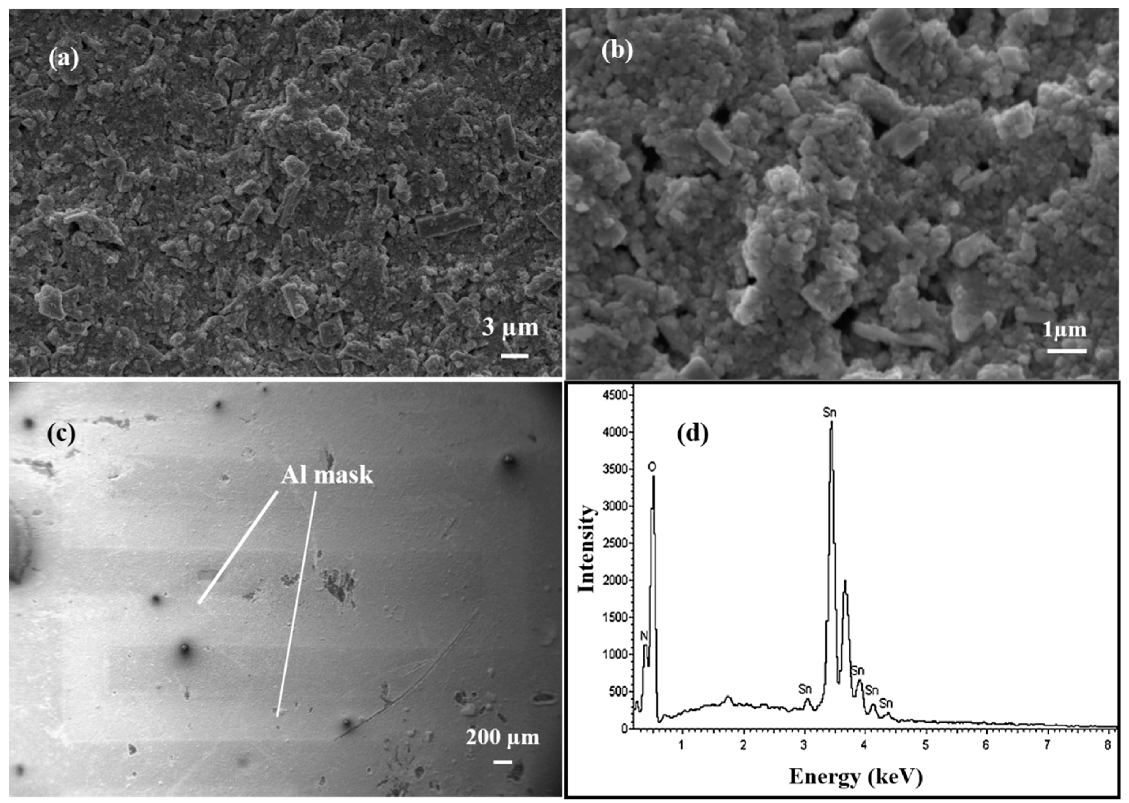
3.2. Microstructural Investigations by Scanning Electron Microscopy

The SEM technique was used to analyse the surface morphology and structural information of the SnO2 thin film (Figure 3a–c). Particles are well connected with each other. The surface of the film is not uniform and possesses porosity, which makes it more sensitive towards gases. The SEM micrographs show the connectivity among particles [22]. In Figure 3c, the aluminium mask used is also visible. An EDS plot for SnO2 is shown in Figure 3d and consists of peaks corresponding to Sn and O.

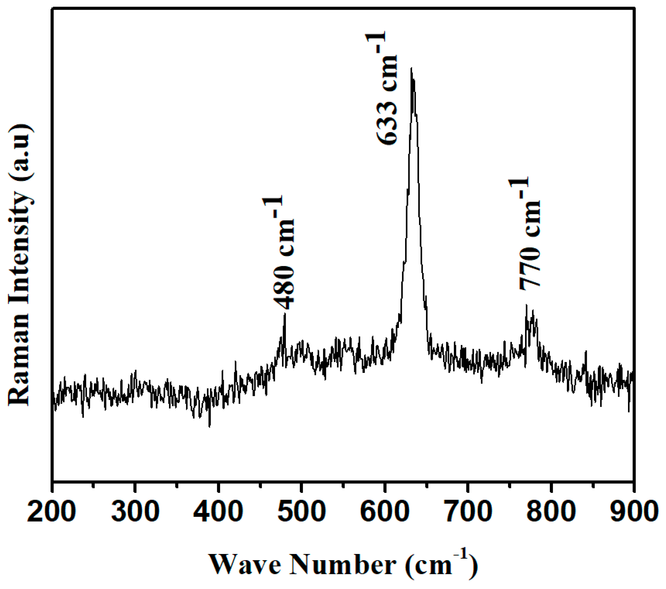
3.3. Raman Spectra of SnO2 Material

In the Raman spectrum, Raman modes have been observed at 480 cm−1, corresponding to O-Sn-O stretching along the molecular axis. Other dominant modes with the highest intense peak have been observed at 633 cm−1 for the acoustic mode (A1g), and one B1g mode has also been observed at 770 cm−1, as shown in Figure 4 [23]. All these modes have demonstrated the formation of SnO2 as proposed from SEM and TEM measurements [24].

3.4. UV Spectroscopy Measurements

The UV measurements were performed to evaluate the electronic bandgap of the SnO2 nanoparticles. Absorbance versus wavelength data obtained from the UV measurement was fitted according to the Tauc plot to reveal whether it follows the direct or indirect bandgap. From the fitting curve, as shown in Figure 5, it is clear that the SnO2 has a direct bandgap because our data has been best fitted with the square of the product of energy and absorbance versus energy corresponding to the incident wavelength. The slope of the curve intersects the energy axis, and the bandgap value is 3.58 eV. However, several low-intensity peaks have been demonstrated near the range of 3.5–4.0 eV, which might be due to the intraband transition and exciton association due to lower energy absorption in comparison to the bandgap of the base material.

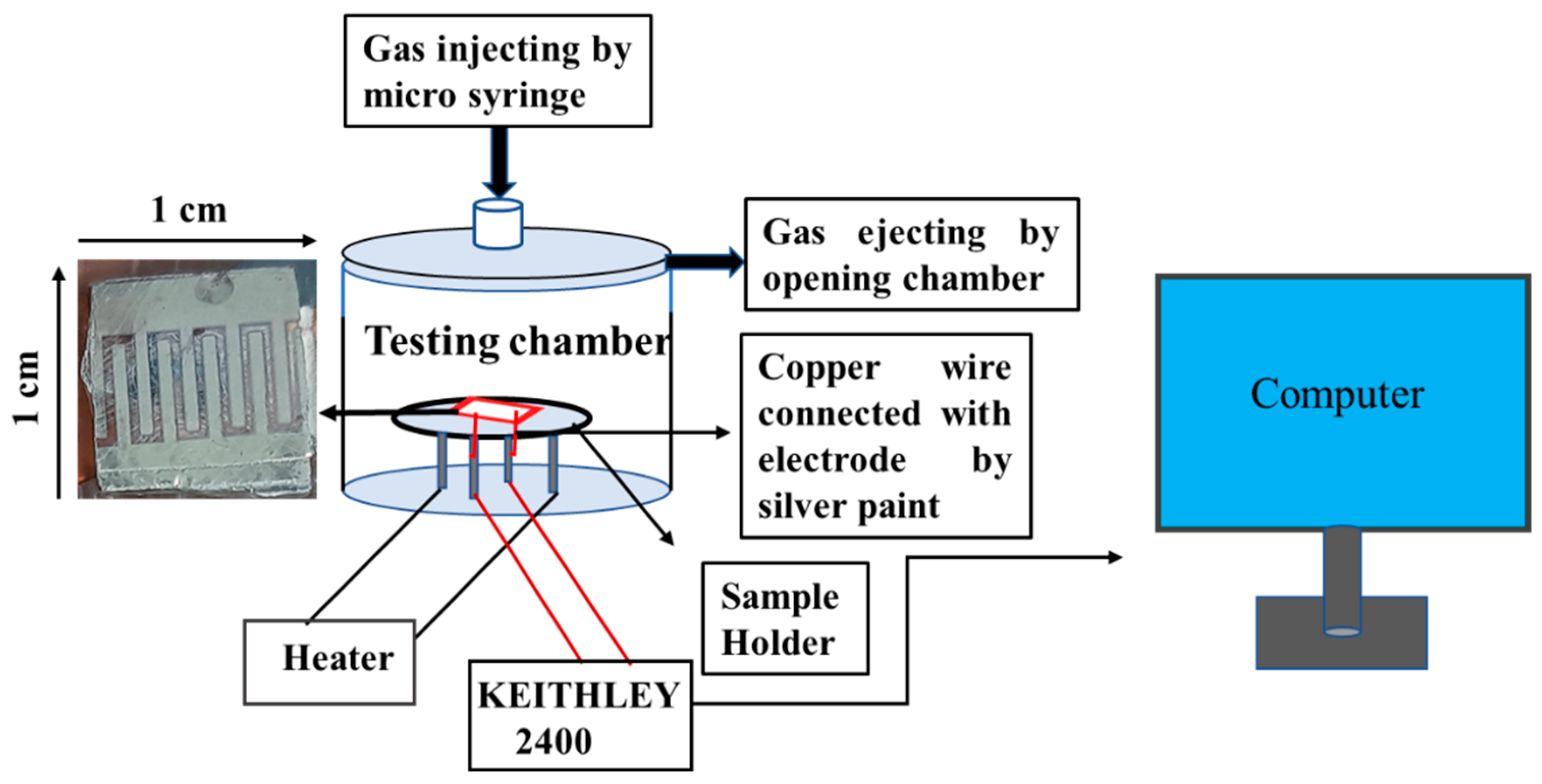
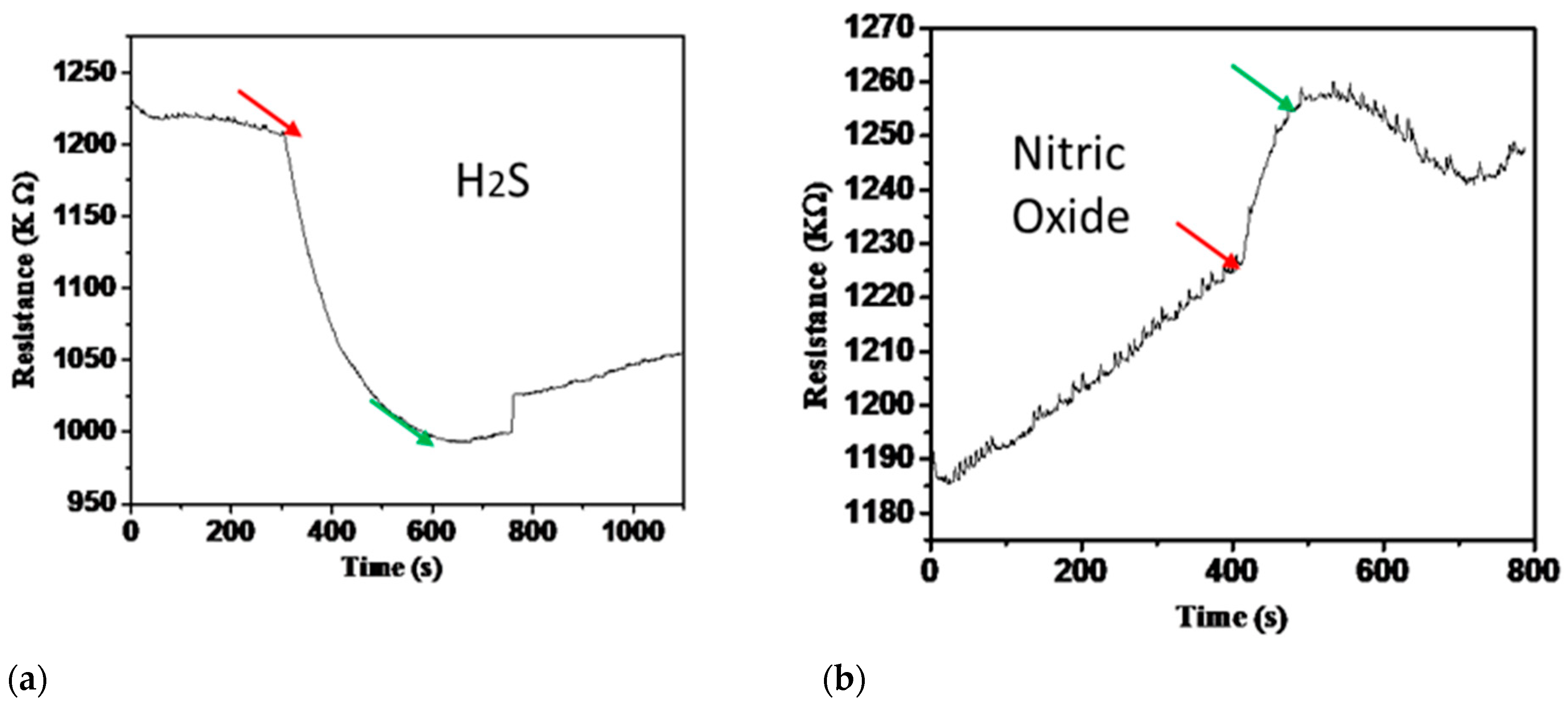
3.5. Gas-Sensing Measurement

A static gas-monitoring system of 250 mL stainless steel was used to test gases made by Ants Innovative Private Limited. NO2 and other gases were injected through a microsyringe at different ppm into the test chamber and measured by using the formula C1V1 = C2V2, where C1 and C2 are concentration of purged gas and the cylinder concentration respectively, and V1 and V2 are the volumes of the test chamber and microsyringe, respectively. The device electrodes were connected by copper wire by high-grade silver paste before carrying out the study for monitoring gas-sensing measurement. The measurement was recorded by a KEITHLEY 2400 source meter. The room temperature condition was 21 °C, and humidity was 60%, measured by a fluke 1620A “Dewk” thermo-hygrometer.
SnO2 is an n-type semiconductor, and NH3, NO, H2S, and NO2 (oxidising gas) were used in the present work. When the device is exposed to the NO2 gas, the resistance increases. The gas-sensing mechanism depends on the adsorption and desorption of NO2 gas (oxidising gas) on the SnO2 (n-type) film surface. NO2 traps the free electrons from the SnO2 surface and increases the sensor resistance. At room temperature, O2 is present on the SnO2 surface, but NO2 gas molecules react directly with Sn ionic sites instead of oxygen species. The reaction is
N O 2 + S n 2 + S n 3 + N O 2 S n 3 + O + N O
The reduction in the concentration of charge carriers from the conduction band of SnO2 upon adsorption results in an increase in sensor resistance. When gas is released due to desorption, the device gains initial condition at room temperature, called recovery.
Researchers have produced NO2 sensors by dropping the dispersion over the electrode to illustrate the sensing application of SnO2–rGO nanocomposites. The SnO2–rGO2 responded to 5 ppm NO2 at operating temperatures ranging from 30 °C to 60 °C [25,26]. In such a case, the NO2 competes with oxygen (O2) in adsorbing onto the surface of SnO2, complicating the oxidation kinetics analysis.
The schematic of the device used in this work is shown in Figure 6, and the SEM of the device is shown in Figure 3c. The change in the resistance at room temperature with the exposure of NO2 is shown in Figure 7. According to the analysis of adsorption–desorption theory, the sensing performance of metal oxide semiconductors can be increased by increasing the gas adsorption site, creating more oxygen vacancies, and boosting the surface activity to catalyse the reaction. The resistance increases as the concentration of NO2 increases, which may be quantified for absolute gas-sensing measurement. The device has almost linear behaviour at room temperature, with a significant change in resistance with a change in gas concentration. The SnO2 gas sensor tested NO2 gas for 0.5 to 2 ppm at room temperature, as shown in Figure 7.
The fluctuation in resistance of metal oxide thin films, when exposed to NO2 gas, makes them ideal for gas sensing. This study describes a novel and simple gas sensor based on SnO2 nano-powder thin films that serve as a physisorption/chemisorption-based sensing element. In the relative gas range, the SnO2 nano-powder thin-film-sensing element with Al masks demonstrates exceptional linear sensing performance for 0.5 to 2 parts per million (0.5, 1, and 2 ppm). Furthermore, at two ppm at ambient temperature, the most incredible sensitivity of 190 was achieved. The presence of oxygen vacancies and the microporous nature of the film allows gas molecules to be absorbed into the film, causing the gas to react at a pace that varies with the amount of gas present. The experimental results show that the thin layer improves sensing capability in SnO2 powder by increasing the surface area of the nanoparticles. SnO2-based sensing elements are resistant to ageing and have highly reproducible properties.
Furthermore, the gas sensor has a response time of 184 s and a recovery time of 432 s at room temperature, which is a relatively swift response. The sensor performance of 1 ppm of H2S, NO, NO2, and NH3 at 150 °C and 1 ppm of NO2 at 50 °C were carried out, and the results are shown in Figure 8a–e. The high-temperature sensing performance of different gases did not fully recover, as shown in Figure 8. The response time improved compared to room temperature NO2 detection, but recovery was not complete. The results of this study and its comparison with other researcher’s results are presented in Table 2.

4. Conclusions

Herein, we have demonstrated a high-performance gas sensor that utilises metal oxide. We used SnO2 as a gas-sensing element to detect various gases (NH3, NO, NO2, and H2S) at various temperatures. The change in resistance is quantified, corresponding to the gas concentration change at room temperature. The fabricated device is selectively sensitive to NO2 gas. The material used is one of Earth’s most abundant materials. The device can be easily fabricated by spin-coating the dispersed SnO2 nano-powder (prepared by sol-gel method) in ethanol on the glass substrate. Its ability to function at room temperature is the device’s primary feature. Overall, from the NO2 measurement and detailed materials property characterisation, we have established that the sensing device with a smaller crystallite size and porosity provides better sensing performance. The sensor showed high sensitivity at 2 ppm with response time and recovery times of 184 s and 432 s for NO2 gas at room temperature. This work can help in producing a low-cost gas-sensing device.

Author Contributions

Conceptualization, methodology, formal analysis, investigation, data curation, visualization and writing—original draft preparation R.K. (Rahul Kumar); investigation and writing—review and editing M., R.K. (Raman Kumari); writing—review and editing and supervision, V.N.S. All authors have read and agreed to the published version of the manuscript.

Funding

This research received no external funding.

Institutional Review Board Statement

Not applicable.

Informed Consent Statement

Not applicable.

Data Availability Statement

Data will be made available upon reasonable request.

Acknowledgments

R.K. would like to acknowledge the director of CSIR (NPL) for providing a facility for doing work and a CSIR-SRF fellowship grant by CSIR-INDIA. We are thankful to Vishal Baloria for providing the system for gas measurement which was part of DST for funding vide IFA16-PH168. We are also thankful for Sumit, Jai Tawale, and Bal Govind for XRD, SEM and Rietveld refinement.

Conflicts of Interest

The authors declare that they have no known competing financial interests or personal relationships that could have appeared to influence the work reported in this paper.

References

  1. Parvatikar, N.; Jain, S.; Khasim, S.; Revansiddappa, M.; Bhoraskar, S.; Prasad, M.A. Electrical and humidity sensing properties of polyaniline/WO3 composites. Sens. Actuators B Chem. 2006, 114, 599–603. [Google Scholar] [CrossRef]
  2. Zhou, L.; Wang, M.; Liu, Z.; Guan, J.; Li, T.; Zhang, D. High-performance humidity sensor based on graphitic carbon nitride/polyethylene oxide and construction of sensor array for non-contact humidity detection. Sens. Actuators B Chem. 2021, 344, 130219. [Google Scholar] [CrossRef]
  3. Kumar, R.; Mamta; Singh, B.P.; Singh, V.N. Exploring the possibility of using MWCNTs sheets as an electrode for flexible room temperature NO2 detection. Superlattices Microstruct. 2022, 164, 107165. [Google Scholar] [CrossRef]
  4. Vanalakar, S.; Patil, V.L.; Patil, S.M.; Dhavale, S.B.; Dongale, T.D.; Patil, P.S. Recent progress in Nanostructured Metal Oxides based NO2 gas sensing in India. J. Mater. NanoSci. 2022, 9, 13–25. [Google Scholar]
  5. Sikarwar, S.; Yadav, B.C.; Singh, S.; Dzhardimalieva, G.I.; Pomogailo, S.I.; Golubeva, N.D.; Pomogailo, A.D. Fabrication of nanostructured yttria stabilised zirconia multilayered films and their optical humidity sens-ing capabilities based on transmission. Sens. Actuators B Chem. 2016, 232, 283–291. [Google Scholar] [CrossRef]
  6. Singh, V.N.; Mehta, B.R.; Joshi, R.K.; Kruis, F.E. Size-dependent gas sensing properties of indium oxide nanoparticle layers. J. Nanosci. Nanotechnol. 2007, 7, 1930–1934. [Google Scholar] [CrossRef]
  7. Kumar, R.; Yadav, B. Humidity sensing investigation on nanostructured polyaniline synthesised via chemical polymerisation method. Mater. Lett. 2016, 167, 300–302. [Google Scholar] [CrossRef]
  8. Krishnakumar, T.; Jayaprakash, R.; Singh, V.; Mehta, B.; Phani, A. Synthesis and Characterization of Tin Oxide Nanoparticle for Humidity Sensor Applications. J. Nano Res. 2008, 4, 91–101. [Google Scholar] [CrossRef]
  9. Chaurasiya, N.; Kumar, U.; Sikarwar, S.; Yadav, B.; Yadawa, P.K. Synthesis of TiO2 nanorods using wet chemical method and their photovoltaic and humidity sensing applications. Sens. Int. 2021, 2, 100095. [Google Scholar] [CrossRef]
  10. Wu, R.-J.; Sun, Y.-L.; Lin, C.-C.; Chen, H.-W.; Chavali, M. Composite of TiO2 nanowires and Nafion as humidity sensor material. Sens. Actuators B Chem. 2006, 115, 198–204. [Google Scholar] [CrossRef]
  11. Yin, H.; Yu, K.; Zhang, Z.; Zeng, M.; Lou, L.; Zhu, Z. Humidity Sensing Properties of Flower-Like VO2(B) and VO2(M) Nanostructures. Electroanalysis 2011, 23, 1752–1758. [Google Scholar] [CrossRef]
  12. Shinde, P.V.; Gagare, S.; Rout, C.S.; Late, D.J. TiO2 nanoflowers based humidity sensor and cytotoxic activity. RSC Adv. 2020, 10, 29378–29384. [Google Scholar] [CrossRef] [PubMed]
  13. Singh, E.; Kumar, U.; Srivastava, R.; Yadav, B.C. Catalytic growth of MWCNT using CVD and its application as opto-electronic humidity sensor. Carbon Lett. 2020, 30, 215–224. [Google Scholar] [CrossRef]
  14. Farzaneh, A.; Mohammadzadeh, A.; Esrafili, M.D.; Mermer, O. Experimental and theoretical study of TiO2 based nanostructured semiconducting humidity sensor. Ceram. Int. 2019, 45, 8362–8369. [Google Scholar] [CrossRef]
  15. Feng, Z.; Wang, S.; Yin, G.; Rajan, R.; Jia, F. Hierarchical SnO2 nanoflower sensitised by BNQDs enhances the gas sensing performances to BTEX. Nano-Technol. 2022, 33, 255602. [Google Scholar]
  16. Aatif, M.; Patel, J.; Sharma, A.; Chauhan, M.; Kumar, G.; Pal, P.; Chand, S.; Tripathi, B.; Pandey, M.K.; Tiwari, J.P. Graphene oxide-molybdenum oxide composite with improved hole transport in bulk heterojunction solar cells. AIP Adv. 2019, 9, 075215. [Google Scholar] [CrossRef] [Green Version]
  17. Rawat, S.S.; Kumar, A.; Srivastava, R.; Suman, C.K. Efficiency Enhancement in Organic Solar Cells by Use of Cobalt Phthalocyanine (CoPc) Thin Films. J. Nanosci. Nanotechnol. 2020, 20, 3703–3709. [Google Scholar] [CrossRef]
  18. Rahman, M.T.; Ahmed, Z.; Islam, M.J.; Khatun, M.T.; Gafur, M.A.; Bashar, M.S.; Alam, M.M. Comparative Study of Structural, Optical and Electrical Properties of SnO2 Thin Film Growth via CBD, Drop-Cast and Dip-Coating Methods. Mater. Sci. Appl. 2021, 12, 578–594. [Google Scholar]
  19. Kong, Y.; Li, Y.; Cui, X.; Su, L.; Ma, D.; Lai, T.; Yao, L.; Xiao, X.; Wang, Y. SnO2 nanostructured materials used as gas sensors for the detection of hazardous and flammable gases: A review. Nano Mater. Sci. 2021, 4, 339–350. [Google Scholar] [CrossRef]
  20. Pi, W.; Chen, X.; Humayun, M.; Yuan, Y.; Lei, Y.; Li, X.; Tang, Z.; Zhang, X.; Huang, D.; Lu, Z.; et al. Sponge-like loose and porous SnO2 microspheres with rich oxygen vacancies and their enhanced room-temperature gas-sensing performance. Nanoscale 2022, 14, 4548–4556. [Google Scholar] [CrossRef]
  21. Govind, B.; Bharti, P.; Srivastava, M.; Kumar, A.; Bano, S.; Bhatt, K.; Tawale, J.; Pulikkotil, J.; Misra, D. Magnetic Properties of Intermediate Ni2-xMn1+xSb Full-Heusler Compounds. Mater. Res. Bull. 2021, 142, 111427. [Google Scholar] [CrossRef]
  22. Govind, B.; Srivastava, M.; Pulikkotil, J.; Misra, D. Electronic structure and magnetic properties of a full-Heusler Mn2NiSb: Cu2MnAl type structure. J. Magn. Magn. Mater. 2021, 517, 167375. [Google Scholar] [CrossRef]
  23. Dariyal, P.; Sharma, S.; Chauhan, G.S.; Singh, B.P.; Dhakate, S.R. Recent trends in gas sensing via carbon nanomaterials: Outlook and challenges. Nanoscale Adv. 2021, 3, 6514–6544. [Google Scholar] [CrossRef]
  24. Wongsaprom, K.; Bornphotsawatkun, R.-A.; Swatsitang, E. Synthesis and characterisation of tin oxide (SnO2) nanocrys-talline powders by a simple modified sol–gel route. Appl. Phys. A 2014, 114, 373–379. [Google Scholar] [CrossRef]
  25. Gervais, F.; Kress, W. Lattice dynamics of oxides with rutile structure and instabilities at the metal-semiconductor phase transitions of NbO2 and VO2. Phys. Rev. B 1985, 31, 4809. [Google Scholar] [CrossRef]
  26. Zhang, H.; Feng, J.; Fei, T.; Liu, S.; Zhang, T. SnO2 nanoparticles-reduced graphene oxide nanocomposites for NO2 sensing at low operating temperature. Sens. Actuators B Chem. 2014, 190, 472–478. [Google Scholar] [CrossRef]
  27. Kumar, R.; Singh, B.; Singh, V. Exploring the possibility of using MWCNTs sheets as an electrode for flexible room tem-perature NO2 detection. Superlattices Microstruct. 2022, 164, 107165. [Google Scholar]
  28. Wang, D.; Zhang, M.; Chen, Z.; Li, H.; Chen, A.; Wang, X.; Yang, J. Enhanced formaldehyde sensing properties of hollow SnO2 nanofibers by graphene oxide. Sens. Actuators B Chem. 2017, 250, 533–542. [Google Scholar] [CrossRef]
  29. Lu, Z.; Zhou, Q.; Wang, C.; Wei, Z.; Xu, L.; Gui, Y. Electrospun ZnO–SnO2 Composite Nanofibers and Enhanced Sensing Properties to SF6 Decomposition Byproduct H2S. Front. Chem. 2018, 6, 540. [Google Scholar] [CrossRef] [PubMed] [Green Version]
  30. Bhangare, B.; Ramgir, N.S.; Pathak, A.; Sinju, K.R.; Debnath, A.K.; Jagtap, S.; Suzuki, N.; Muthe, K.P.; Terashima, C.; Aswal, D.K.; et al. Role of sensitisers in imparting the selective response of SnO2/RGO based nanohybrids towards H2S, NO2 and H2. Mater. Sci. Semicond. Process. 2020, 105, 104726. [Google Scholar] [CrossRef]
  31. Masuda, Y. Recent advances in SnO2 nanostructure based gas sensors. Sens. Actuators B Chem. 2022, 364, 131876. [Google Scholar] [CrossRef]
  32. Park, J.-A.; Moon, J.; Lee, S.-J.; Kim, S.H.; Chu, H.Y.; Zyung, T. SnO2–ZnO hybrid nanofibers-based highly sensitive nitrogen dioxides sensor. Sens. Actuators B Chem. 2010, 145, 592–595. [Google Scholar] [CrossRef]
  33. Tang, H.; Gao, C.; Yang, H.; Sacco, L.; Sokolovskij, R.; Zheng, H.; Ye, H.; Vollebregt, S.; Yu, H.; Fan, X.; et al. Room temperature ppt-level NO2 gas sensor based on SnOx/SnS nanostructures with rich oxygen vacancies. 2D Mater. 2021, 8, 045006. [Google Scholar] [CrossRef]
  34. Kaur, J.; Roy, S.C.; Bhatnagar, M. Highly sensitive SnO2 thin film NO2 gas sensor operating at low temperature. Sens. Actuators B Chem. 2007, 123, 1090–1095. [Google Scholar] [CrossRef]
  35. Hyodo, T.; Urata, K.; Kamada, K.; Ueda, T.; Shimizu, Y. Semiconductor-type SnO2-based NO2 sensors operated at room temperature under UV-light irradiation. Sens. Actuators B Chem. 2017, 253, 630–640. [Google Scholar] [CrossRef] [Green Version]
  36. Choi, Y.J.; Hwang, I.-S.; Park, J.-G.; Choi, K.J.; Park, J.H.; Lee, J.-H. Novel fabrication of an SnO2 nanowire gas sensor with high sensitivity. Nanotechnology 2008, 19, 095508. [Google Scholar] [CrossRef]
  37. Devabharathi, N.; Umarji, A.M.; Dasgupta, S. Fully inkjet-printed mesoporous SnO2-based ultrasensitive gas sensors for trace amount NO2 detection. ACS Appl. Mater. Interfaces 2020, 12, 57207–57217. [Google Scholar] [CrossRef] [PubMed]
  38. Sharma, A.; Tomar, M.; Gupta, V. SnO2 thin film sensor with enhanced response for NO2 gas at lower temperatures. Sens. Actuators B Chem. 2011, 156, 743–752. [Google Scholar] [CrossRef]
Figure 1. (a) XRD patterns of SnO2 nano-powder with indexed diffraction peaks corresponding to standard JCPDS data card (41-1445). (b) W-H plot of the synthesised material. (c) Refinement of SnO2 compared with the standard Bragg position. (d) Schematic diagram of a unit cell of SnO2 originated using Vesta software. (e) Schematic diagram of the fabrication of the device.
Micromachines 14 00728 g001
Figure 2. (a) TEM image of sensing base material. (b) Histogram analysed by Image-J software. (c) HRTEM image of nanoparticles. (d) Shows a different plane in the SAED pattern.
Micromachines 14 00728 g002
Figure 3. (ac) 6 SEM image of the SnO2 thin film at different magnifications. (d) EDS of the tin oxide film.
Micromachines 14 00728 g003
Figure 4. Raman spectra of SnO2 nano-powder.
Micromachines 14 00728 g004
Figure 5. UV spectroscopy for the confirmation of the SnO2 band gap.
Micromachines 14 00728 g005
Figure 6. Schematic diagram of gas monitoring set up with the fabricated device.
Micromachines 14 00728 g006
Figure 7. The sensor response of the SnO2 device at room temperature at different concentrations of 0.5, 1, and 2 ppm of NO2 at room temperature.
Micromachines 14 00728 g007
Figure 8. (ad) The sensor performance of 1 ppm of H2S, NO, NO2, and NH3 at 150 °C. (e) -Sensor response for one ppm of NO2 at 50 °C.
Micromachines 14 00728 g008aMicromachines 14 00728 g008b
Table 1. Parameters of analysed XRD spectra.
Lattice Parameters (Å)a = 4.739, b = 4.739, c = 3.1879
Angle α = 90 ° , β = 90°, γ = 90°
χ 20.083
Volume (Å)371.959
Table 2. Comparison table for different gases and materials.
S. No.MaterialsExperimental ProcessMeasuring Temperature (°C/Gas (ppm)Sensing ParameterReferences
Sensitivity
(S = Rg − Ra/Ra) × 100
Response Time (s)Recovery Time (s)
1SnO2Sol-gel, spin-coating, annealing,RT/NO2 (0.5)5084320This work
2SnO2Sol-gel, spin-coating, annealingRT/NO2 (1) 102124284This work
3SnO2Sol-gel, spin-coating, annealingRT/NO2 (2)190184432This work
4SnO2Sol-gel, spin-coating, annealing150 °C/H2S (1)21234NoThis work
5SnO2Sol-gel, spin-coating, annealing150 °C/NO (1)264noThis work
6SnO2Sol-gel, spin-coating, annealing150 °C/NO2 (1)1760nThis work
7SnO2Sol-gel, spin-coating, annealing50 °C/NO2 (1)5374NoThis work
8SnO2Sol-gel, spin-coating, annealing150 °C/NH3(1)1650noThis work
9GO/SnO2 nanocompositesElectro-spinning and calcination procedure120 °C/Formaldehyde (100)-32-[27]
10Ni doping of SnO2 nanoparticlesHydrothermal method200 °C/Formaldehyde (100)-130-[28]
11SnO2–rGO; Pd hydrogel -200 °C/NO2 (4)1858-[29]
12SnO2–ZnO-200 °C/NO2 (400 ppb)-300300[30]
13SnO2/Graphene-150 °C/NO2(10 ppb)-43408[31]
14SnO2/SnS-25 °C/NO2 (1 ppb)-180036 (UV)[32]
15SnO2/SnS-25 °C/NO2-180036 (UV)[33]
16 SnO2 filmSol-gel100 °C/NO2 (500 ppm)10 (response)--[34]
17SnO2Sol-gelUV radiation/NO2 (5 ppm)360 (response)276-[35]
18SnO2Thermal evaporation200 °C/NO2 (0.5 ppm)-4318[36]
19SnO2Sputtering100 °C/NO2 (50 ppm)4300 (response)1261152[37]
20Mesoporous SnO2Inkjet printing175 °C/NO2 (5 ppm)11,507 (response)--[38]
Disclaimer/Publisher’s Note: The statements, opinions and data contained in all publications are solely those of the individual author(s) and contributor(s) and not of MDPI and/or the editor(s). MDPI and/or the editor(s) disclaim responsibility for any injury to people or property resulting from any ideas, methods, instructions or products referred to in the content.

