
Quantitative Field Emission Imaging for Studying the Doping-Dependent Emission Behavior of Silicon Field Emitter Arrays

 , , , and
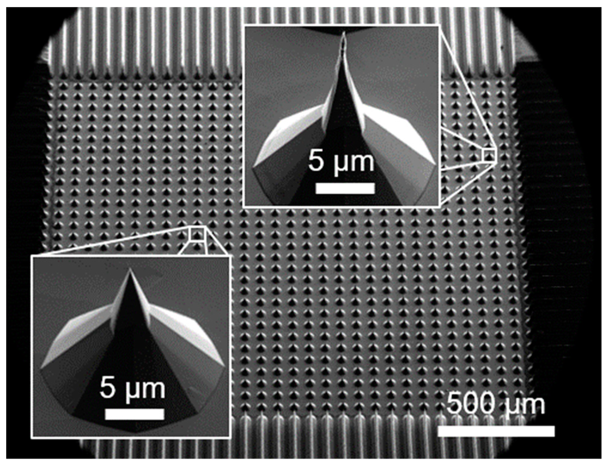
Abstract
1. Introduction
2. Materials and Methods
3. Results and Discussion
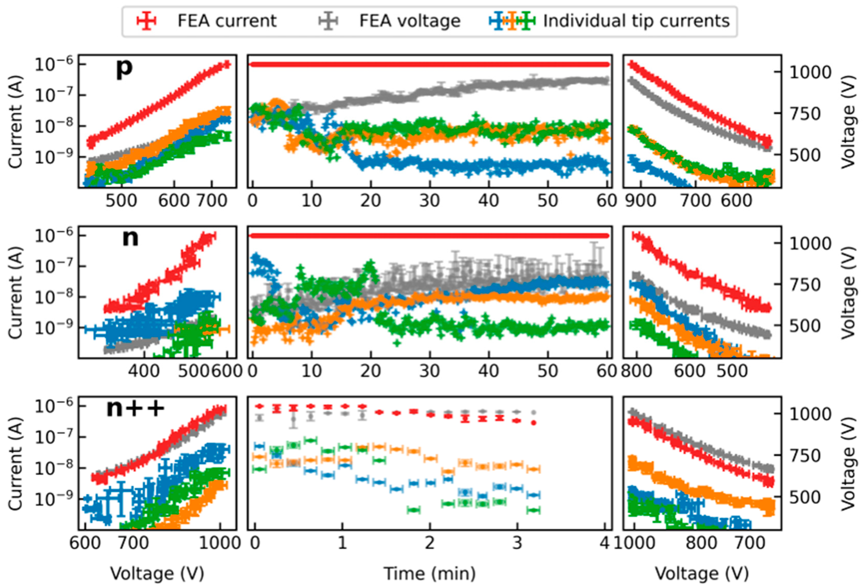
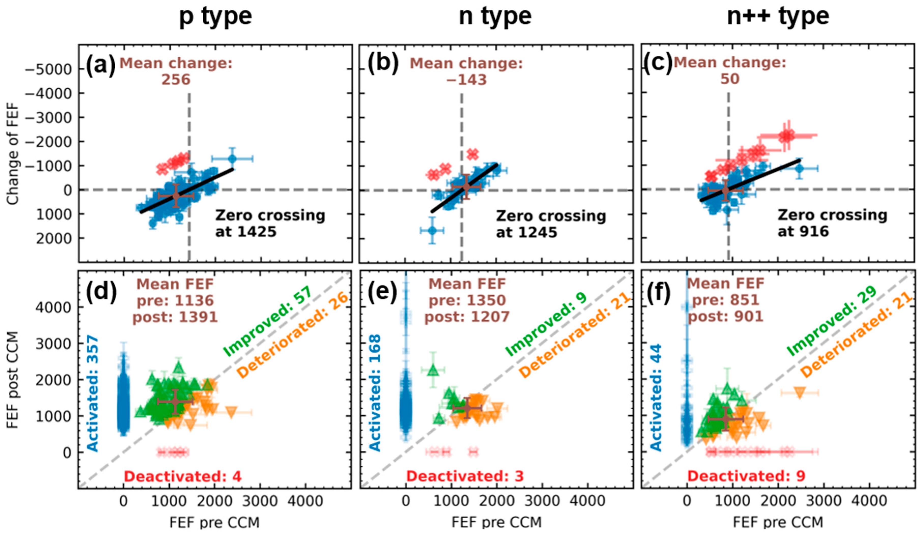
3.1. Integral Measurements and Single-Tip Emissions
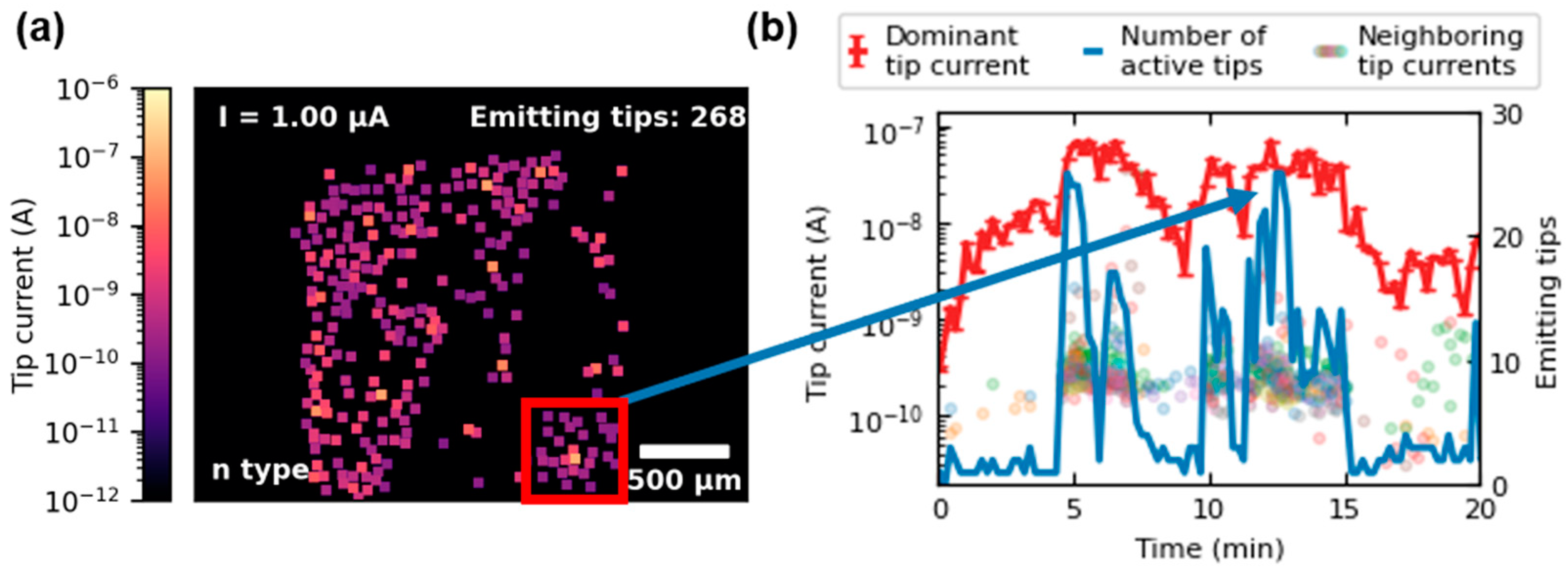
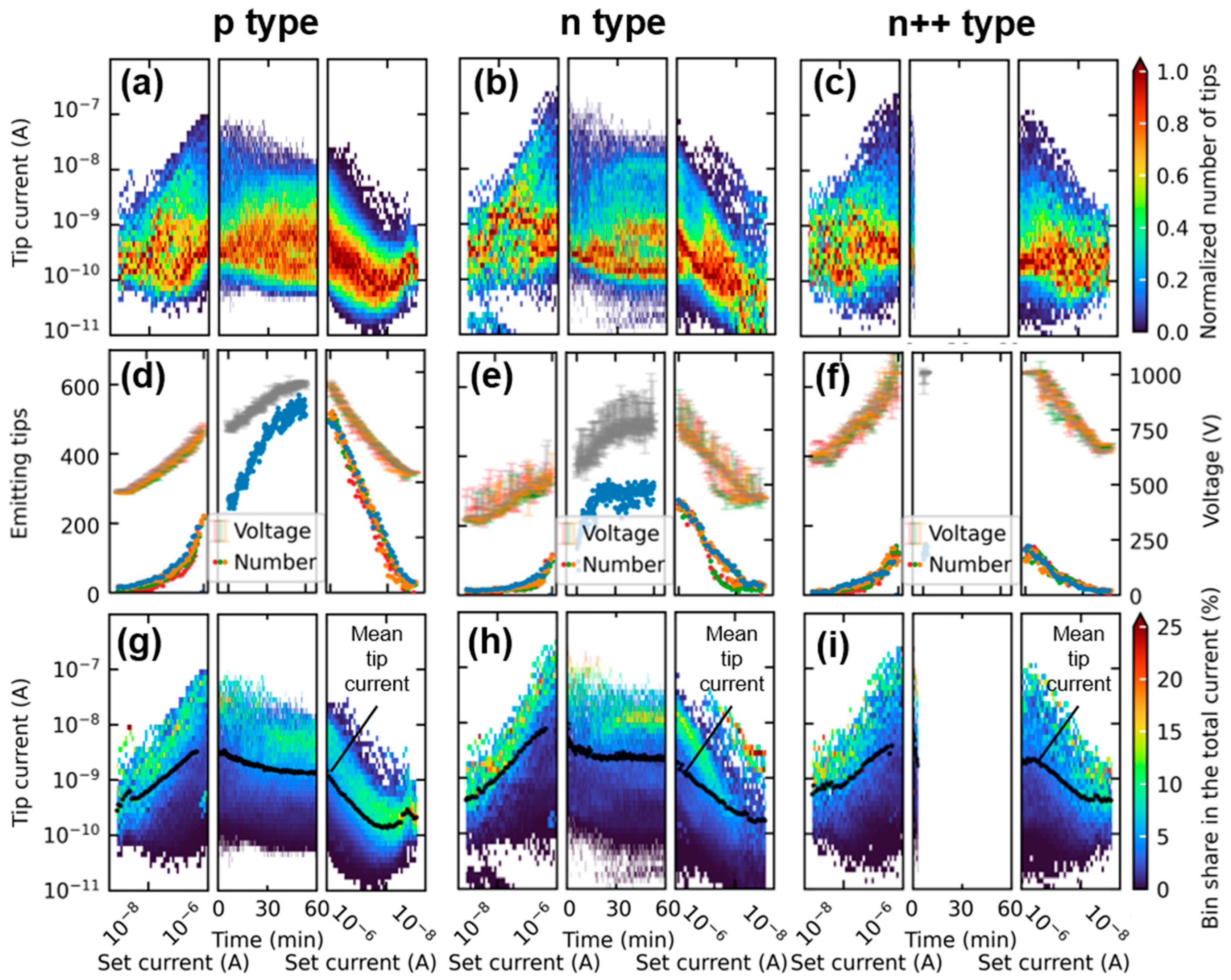
3.2. Change of Current Distribution during the Measurement
3.3. Individual Tip IV Characteristics
4. Conclusions
Author Contributions
Funding
Data Availability Statement
Conflicts of Interest
References
- Diop, B.; Binh, V.T. Quasi-Monochromatic Field-Emission X-ray Source. Rev. Sci. Instrum. 2012, 83, 094704. [Google Scholar] [CrossRef] [PubMed]
- Shao, X.; Srinivasan, A.; Ang, W.K.; Khursheed, A. A High-Brightness Large-Diameter Graphene Coated Point Cathode Field Emission Electron Source. Nat. Commun. 2018, 9, 1288. [Google Scholar] [CrossRef] [PubMed]
- Serbun, P.; Porshyn, V.; Müller, G.; Lützenkirchen-Hecht, D. Advanced Field Emission Measurement Techniques for Research on Modern Cold Cathode Materials and Their Applications for Transmission-Type X-ray Sources. Rev. Sci. Instrum. 2020, 91, 083906. [Google Scholar] [CrossRef] [PubMed]
- Fransen, M.; van Rooy, T.; Kruit, P. Field Emission Energy Distributions from Individual Multiwalled Carbon Nanotubes. Appl. Surf. Sci. 1999, 146, 312–327. [Google Scholar] [CrossRef]
- Basu, A.; Swanwick, M.E.; Fomani, A.A.; Velásquez-García, L.F. A Portable X-ray Source with a Nanostructured Pt-Coated Silicon Field Emission Cathode for Absorption Imaging of Low-Z Materials. J. Phys. D Appl. Phys. 2015, 48, 225501. [Google Scholar] [CrossRef]
- Bugaev, A.S.; Eroshkin, P.A.; Romanko, V.A.; Sheshin, E.P. Low-Power X-Ray Tubes (the Current State). Phys.-Uspekhi 2013, 56, 691–703. [Google Scholar] [CrossRef]
- Whaley, D.R.; Duggal, R.; Armstrong, C.M.; Bellew, C.L.; Holland, C.E.; Spindt, C.A. 100 W Operation of a Cold Cathode TWT. IEEE Trans. Electron Devices 2009, 56, 896–905. [Google Scholar] [CrossRef]
- Gupta, A.P.; Park, S.; Yeo, S.J.; Jung, J.; Cho, C.; Paik, S.H.; Park, H.; Cho, Y.C.; Kim, S.H.; Shin, J.H.; et al. Direct Synthesis of Carbon Nanotube Field Emitters on Metal Substrate for Open-Type X-ray Source in Medical Imaging. Materials 2017, 10, 878. [Google Scholar] [CrossRef]
- Cole, M.T.; Parmee, R.J.; Milne, W.I. Nanomaterial-Based X-ray Sources. Nanotechnology 2016, 27, 082501. [Google Scholar] [CrossRef]
- Whaley, D.R.; Gannon, B.M.; Smith, C.R.; Armstrong, C.M.; Spindt, C.A. Application of Field Emitter Arrays to Microwave Power Amplifiers. IEEE Trans. Plasma Sci. 2000, 28, 727–747. [Google Scholar] [CrossRef]
- Liu, W.; Liu, Y.; Jia, Q.; Sun, B.; Chen, J. Terahertz Laser Diode Using Field Emitter Arrays. Phys. Rev. B 2021, 103, 035109. [Google Scholar] [CrossRef]
- Han, J.W.; Seol, M.L.; Kim, J.; Meyyappan, M. Nanoscale Complementary Vacuum Field Emission Transistor. ACS Appl. Nano Mater. 2020, 3, 11481–11488. [Google Scholar] [CrossRef]
- Bhattacharya, R.; Hay, R.; Cannon, M.; Karaulac, N.; Rughoobur, G.; Akinwande, A.I.; Browning, J. Demonstration of a Silicon Gated Field Emitter Array Based Low Frequency Colpitts Oscillator at 400 °C. J. Vac. Sci. Technol. B 2023, 41, 023201. [Google Scholar] [CrossRef]
- Kolosko, A.G.; Filippov, S.V.; Popov, E.O. Vacuum Discharge Analysis of CNT Field Cathode Using a Computerized Field Projector. J. Vac. Sci. Technol. B 2023, 41, 032801. [Google Scholar] [CrossRef]
- Browning, J.; McGruer, N.E.; Meassick, S.; Chan, C.; Bintz, W.J.; Gilmore, M. Gated Field Emitter Failures: Experiment and Theory. IEEE Trans. Plasma Sci. 1992, 20, 499–506. [Google Scholar] [CrossRef]
- Browning, J.; McGruer, N.E.; Bintz, W.J.; Gilmore, M. Experimental Observations of Gated Field Emitter Failures. IEEE Electron Device Lett. 1992, 13, 167–169. [Google Scholar] [CrossRef]
- Chen, L.; Yu, H.; Zhong, J.; Song, L.; Wu, J.; Su, W. Graphene Field Emitters: A Review of Fabrication, Characterization and Properties. Mater. Sci. Eng. B 2017, 220, 44–58. [Google Scholar] [CrossRef]
- Kim, J.W.; Jeong, J.W.; Kang, J.T.; Choi, S.; Ahn, S.; Song, Y.H. Highly Reliable Field Electron Emitters Produced from Reproducible Damage-Free Carbon Nanotube Composite Pastes with Optimal Inorganic Fillers. Nanotechnology 2014, 25, 065201. [Google Scholar] [CrossRef]
- Bachmann, M.; Düsberg, F.; Pahlke, A.; Edler, S.; Schels, A.; Herdl, F.; Ławrowski, R.; Schreiner, R. High Current Silicon Nanowire Field Emitter Arrays. J. Vac. Sci. Technol. B 2022, 40, 010605. [Google Scholar] [CrossRef]
- Guerrera, S.A.; Akinwande, A.I. Silicon Field Emitter Arrays with Current Densities Exceeding 100 A/cm2 at Gate Voltages Below 75 V. IEEE Electron Device Lett. 2016, 37, 96–99. [Google Scholar] [CrossRef]
- Hausladen, M.; Buchner, P.; Schels, A.; Edler, S.; Bachmann, M.; Schreiner, R. An Integrated Field Emission Electron Source on a Chip Fabricated by Laser-Micromachining and Mems Technology. In Proceedings of the 2023 IEEE 36th International Vacuum Nanoelectronics Conference (IVNC), Cambridge, MA, USA, 10–13 July 2023; IEEE: Piscataway, NJ, USA, 2023; pp. 115–116. [Google Scholar]
- Niu, Z.; Zhu, M.; Bellotti, E. Three-Dimensional Monte Carlo Simulation of Silicon Field Emitters. IEEE Trans. Electron Devices 2023, 70, 4379–4386. [Google Scholar] [CrossRef]
- Liu, W.; Zeng, F.; Xin, L.; Zhu, C.; He, Y. Turn-on Field Distribution of Field-Emitting Sites in Carbon Nanotube Film: Study with Luminescent Image. J. Vac. Sci. Technol. B Microelectron. Nanomater Struct. 2008, 26, 32. [Google Scholar] [CrossRef]
- Filippov, S.V.; Popov, E.O.; Kolosko, A.G.; Vinnichek, R.N. Evaluation of Numerical Characteristics of the Current Load Distribution on the Surface of Multi-Tip Field Emitters. J. Phys. Conf. Ser. 2017, 917, 092022. [Google Scholar] [CrossRef]
- Popov, E.O.; Kolosko, A.G.; Filippov, S.V.; Terukov, E.I. Local Current–Voltage Estimation and Characteristization Based on Field Emission Image Processing of Large-Area Field Emitters. J. Vac. Sci. Technol. B Nanotechnol. Microelectron. Mater. Process. Meas. Phenom. 2018, 36, 02C106. [Google Scholar] [CrossRef]
- Nilsson, L.; Groening, O.; Kuettel, O.; Groening, P.; Schlapbach, L. Microscopic Characterization of Electron Field Emission. J. Vac. Sci. Technol. B Microelectron. Nanomater Struct. 2002, 20, 326. [Google Scholar] [CrossRef][Green Version]
- Tsujino, S. On the Brightness, Transverse Emittance, and Transverse Coherence of Field Emission Beam. J. Vac. Sci. Technol. B 2022, 40, 030801. [Google Scholar] [CrossRef]
- Sun, Y.; Shin, D.H.; Yun, K.N.; Hwang, Y.M.; Song, Y.; Leti, G.; Jeon, S.-G.; Kim, J.-I.; Saito, Y.; Lee, C.J. Field Emission Behavior of Carbon Nanotube Field Emitters after High Temperature Thermal Annealing. AIP Adv. 2014, 4, 077110. [Google Scholar] [CrossRef]
- Serbun, P.; Bornmann, B.; Navitski, A.; Müller, G.; Prommesberger, C.; Langer, C.; Dams, F.; Schreiner, R. Stable Field Emission of Single B-Doped Si Tips and Linear Current Scaling of Uniform Tip Arrays for Integrated Vacuum Microelectronic Devices. J. Vac. Sci. Technol. B Nanotechnol. Microelectron. Mater. Process. Meas. Phenom. 2013, 31, 02B101. [Google Scholar] [CrossRef]
- Shang, C.; Wang, X.; Cheng, Z.; Hou, Z.; Lin, J. Mechanisms in the Saturation Behavior for Low Voltage Cathodoluminescence. J. Appl. Phys. 2013, 113, 093101. [Google Scholar] [CrossRef]
- Rughoobur, G.; Ilori, O.O.; Akinwande, A.I. Scanning Anode Field Emission Microscopy of a Single Si Emitter. J. Vac. Sci. Technol. B 2022, 40, 042803. [Google Scholar] [CrossRef]
- Nilsson, L.; Groening, O.; Emmenegger, C.; Kuettel, O.; Schaller, E.; Schlapbach, L.; Kind, H.; Bonard, J.-M.M.; Kern, K. Scanning Field Emission from Patterned Carbon Nanotube Films. Appl. Phys. Lett. 2000, 76, 2071–2073. [Google Scholar] [CrossRef]
- Nilsson, L.; Groening, O.; Groening, P.; Kuettel, O.; Schlapbach, L. Characterization of Thin Film Electron Emitters by Scanning Anode Field Emission Microscopy. J. Appl. Phys. 2001, 90, 768–780. [Google Scholar] [CrossRef][Green Version]
- Chen, G.; Zhao, B.; Kimura, H.; Kurachi, H.; Matsumoto, N.; Yamada, T.; Hata, K.; Uemura, S.; Futaba, D.N. Low Turn-on and Uniform Field Emission from Structurally Engineered Carbon Nanotube Arrays through Growth on Metal Wire Mesh Substrates. Mater. Res. Express 2017, 4, 105041. [Google Scholar] [CrossRef]
- Kurachi, H.; Uemura, S.; Yotani, J.; Nagasako, T.; Yamada, H.; Ezaki, T.; Maesoba, T.; Nakao, T.; Ito, M.; Sakurai, A.; et al. Uniform Carbon-Nanotube Emitter for Field-Emission Displays. J. Soc. Inf. Disp. 2005, 13, 727. [Google Scholar] [CrossRef]
- Schels, A.; Edler, S.; Herdl, F.; Hansch, W.; Bachmann, M.; Ritter, D.; Dudeck, M.; Düsberg, F.; Meyer, M.; Pahlke, A.; et al. In Situ Quantitative Field Emission Imaging Using a Low-Cost CMOS Imaging Sensor. J. Vac. Sci. Technol. B 2022, 40, 014202. [Google Scholar] [CrossRef]
- Edler, S.; Schels, A.; Biba, J.; Hansch, W.; Bachmann, M.; Düsberg, F.; Werber, M.; Langer, C.; Meyer, M.; von Bergen, D.; et al. Silicon Field Emitters Fabricated by Dicing-Saw and Wet-Chemical-Etching. J. Vac. Sci. Technol. B Nanotechnol. Microelectron. Mater. Process. Meas. Phenom. 2021, 39, 013205. [Google Scholar] [CrossRef]
- Sony Semiconductor Solutions Coopera-tion Data Sheet IMX477-AACK-C. Sony Semiconductor Solutions Cooperation. Available online: https://www.uctronics.com/download/Image_Sensor/IMX477-%0ADS.pdf (accessed on 31 July 2023).
- Prommesberger, C.; Bachmann, M.; Dusberg, F.; Langer, C.; Lawrowski, R.; Hofmann, M.; Pahlke, A.; Schreiner, R. Regulation of the Transmitted Electron Flux in a Field-Emission Electron Source Demonstrated on Si Nanowhisker Cathodes. IEEE Trans. Electron Devices 2017, 64, 5128–5133. [Google Scholar] [CrossRef]
- Schels, A.; Herdl, F.; Hausladen, M.; Wohlfartsstätter, D.; Bachmann, M.; Edler, S.; Düsberg, F.; Pahlke, A.; Buchner, P.; Schreiner, R.; et al. Beta Factor Mapping of Individual Emitting Tips During Integral Operation of Field Emission Arrays. In Proceedings of the 2023 IEEE 36th International Vacuum Nanoelectronics Conference (IVNC), Cambridge, MA, USA, 10–13 July 2023; IEEE: Piscataway, NJ, USA, 2023; pp. 224–226. [Google Scholar]
- Forbes, R.G. The Murphy–Good Plot: A Better Method of Analysing Field Emission Data. R. Soc. Open Sci. 2019, 6, 190912. [Google Scholar] [CrossRef]
- Forbes, R.G. Use of Millikan-Lauritsen Plots, Rather than Fowler-Nordheim Plots, to Analyze Field Emission Current-Voltage Data. J. Appl. Phys. 2009, 105, 114313. [Google Scholar] [CrossRef]
- Edler, S.; Schels, A.; Herdl, F.; Hansch, W.; Bachmann, M.; Dudeck, M.; Düsberg, F.; Pahlke, A.; Hausladen, M.; Buchner, P.; et al. Origin of the Current Saturation Level of P-Doped Silicon Field Emitters. J. Vac. Sci. Technol. B 2022, 40, 013203. [Google Scholar] [CrossRef]
- Fursey, G.; Brodie, I.; Schwoebel, P. Field Emission in Vacuum Microelectronics; Brodie, I., Schwoebel, P., Eds.; Microdevices; Springer US: Boston, MA, USA, 2005; ISBN 978-0-306-47450-7. [Google Scholar]
- Liu, K.X.; Chiang, C.-J.; Heritage, J.P. Photoresponse of Gated P-Silicon Field Emitter Array and Correlation with Theoretical Models. J. Appl. Phys. 2006, 99, 034502. [Google Scholar] [CrossRef]
- Edler, S.; Bachmann, M.; Breuer, J.; Dams, F.; Düsberg, F.; Hofmann, M.; Jakšič, J.; Pahlke, A.; Langer, C.; Ławrowski, R.; et al. Influence of Adsorbates on the Performance of a Field Emitter Array in a High Voltage Triode Setup. J. Appl. Phys. 2017, 122, 124503. [Google Scholar] [CrossRef]
- Jensen, K.L.; Marrese-Reading, C.M. Emission Statistics and the Characterization of Array Current. J. Vac. Sci. Technol. B Microelectron. Nanomater Struct. Process. Meas. Phenom. 2003, 21, 412–417. [Google Scholar] [CrossRef]
- Ding, M.; Sha, G.; Akinwande, A.I. Silicon Field Emission Arrays with Atomically Sharp Tips: Turn-on Voltage and the Effect of Tip Radius Distribution. IEEE Trans. Electron Devices 2002, 49, 2333–2342. [Google Scholar] [CrossRef]
- Velásquez-García, L.F.; Guerrera, S.A.; Niu, Y.; Akinwande, A.I. Uniform High-Current Cathodes Using Massive Arrays of Si Field Emitters Individually Controlled by Vertical Si Ungated FETs-Part 1: Device Design and Simulation. IEEE Trans. Electron Devices 2011, 58, 1775–1782. [Google Scholar] [CrossRef]
- Forbes, R.G.; Edgcombe, C.J.; Valdrè, U. Some Comments on Models for Field Enhancement. Ultramicroscopy 2003, 95, 57–65. [Google Scholar] [CrossRef] [PubMed]
- Biswas, D. A Universal Formula for the Field Enhancement Factor. Phys. Plasmas 2018, 25, 043113. [Google Scholar] [CrossRef]
- Biswas, D.; Singh, G.; Sarkar, S.G.; Kumar, R. Variation of Field Enhancement Factor near the Emitter Tip. Ultramicroscopy 2018, 185, 1–4. [Google Scholar] [CrossRef]


Disclaimer/Publisher’s Note: The statements, opinions and data contained in all publications are solely those of the individual author(s) and contributor(s) and not of MDPI and/or the editor(s). MDPI and/or the editor(s) disclaim responsibility for any injury to people or property resulting from any ideas, methods, instructions or products referred to in the content. |
© 2023 by the authors. Licensee MDPI, Basel, Switzerland. This article is an open access article distributed under the terms and conditions of the Creative Commons Attribution (CC BY) license (https://creativecommons.org/licenses/by/4.0/).
Share and Cite
Schels, A.; Herdl, F.; Hausladen, M.; Wohlfartsstätter, D.; Edler, S.; Bachmann, M.; Pahlke, A.; Schreiner, R.; Hansch, W. Quantitative Field Emission Imaging for Studying the Doping-Dependent Emission Behavior of Silicon Field Emitter Arrays. Micromachines 2023, 14, 2008. https://doi.org/10.3390/mi14112008
Schels A, Herdl F, Hausladen M, Wohlfartsstätter D, Edler S, Bachmann M, Pahlke A, Schreiner R, Hansch W. Quantitative Field Emission Imaging for Studying the Doping-Dependent Emission Behavior of Silicon Field Emitter Arrays. Micromachines. 2023; 14(11):2008. https://doi.org/10.3390/mi14112008
Chicago/Turabian StyleSchels, Andreas, Florian Herdl, Matthias Hausladen, Dominik Wohlfartsstätter, Simon Edler, Michael Bachmann, Andreas Pahlke, Rupert Schreiner, and Walter Hansch. 2023. "Quantitative Field Emission Imaging for Studying the Doping-Dependent Emission Behavior of Silicon Field Emitter Arrays" Micromachines 14, no. 11: 2008. https://doi.org/10.3390/mi14112008
APA StyleSchels, A., Herdl, F., Hausladen, M., Wohlfartsstätter, D., Edler, S., Bachmann, M., Pahlke, A., Schreiner, R., & Hansch, W. (2023). Quantitative Field Emission Imaging for Studying the Doping-Dependent Emission Behavior of Silicon Field Emitter Arrays. Micromachines, 14(11), 2008. https://doi.org/10.3390/mi14112008