
Measurement and Simulation of Ultra-Low-Energy Ion–Solid Interaction Dynamics
 , , , , and
Abstract
:1. Introduction
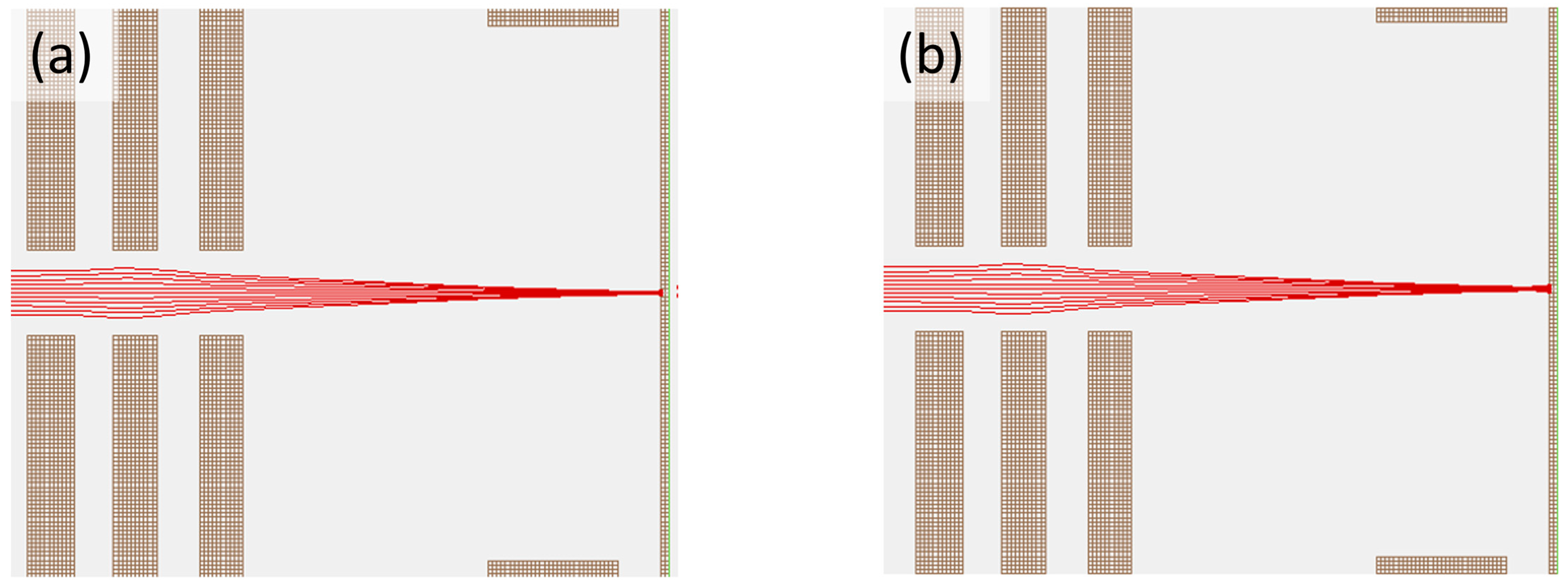
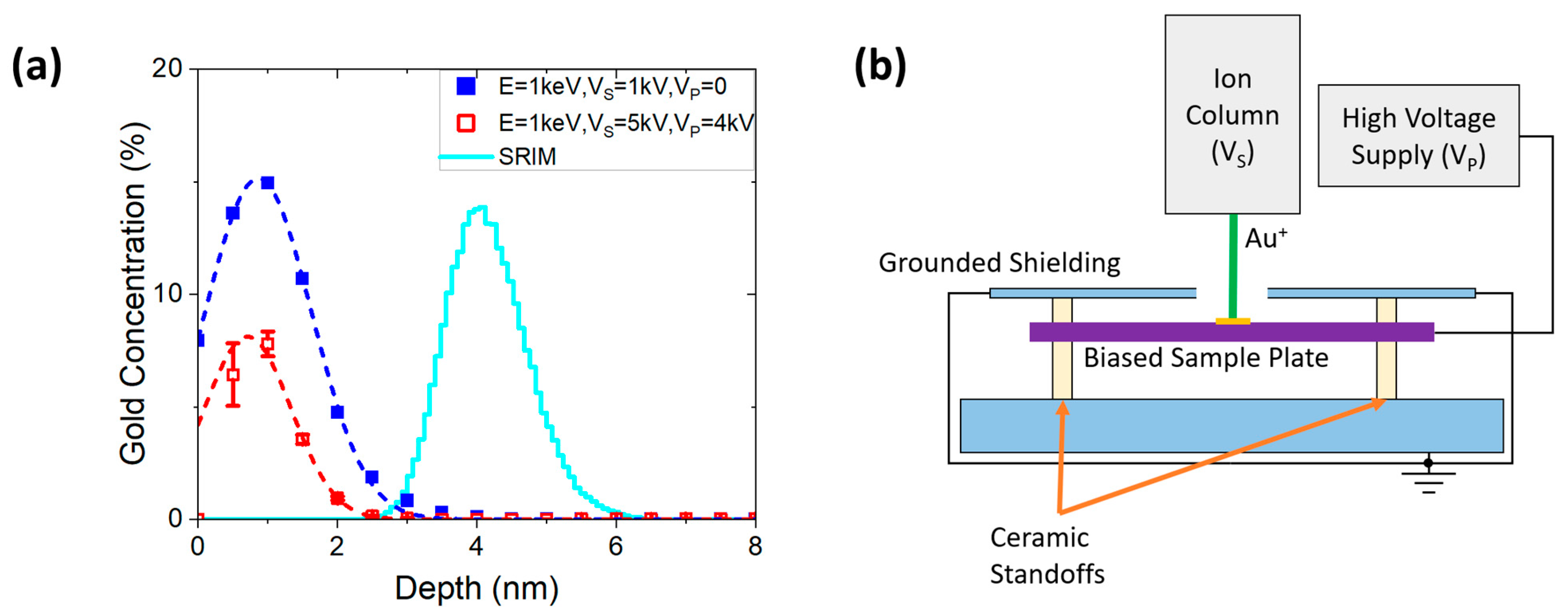
2. Methods
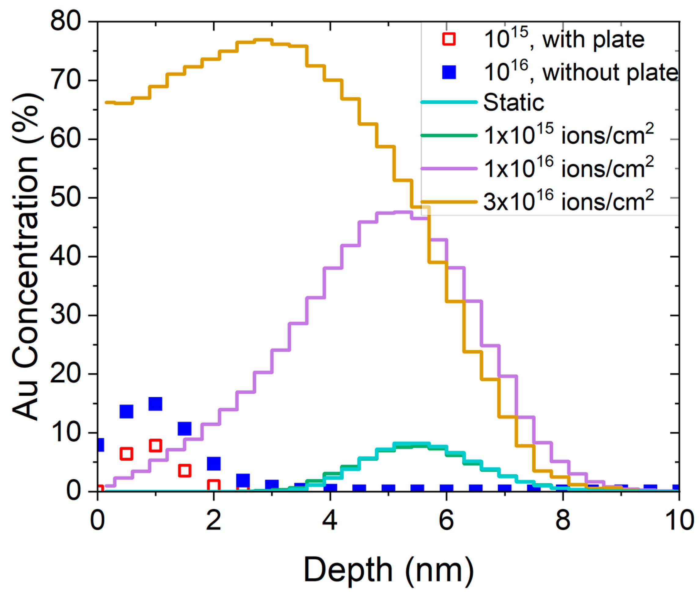
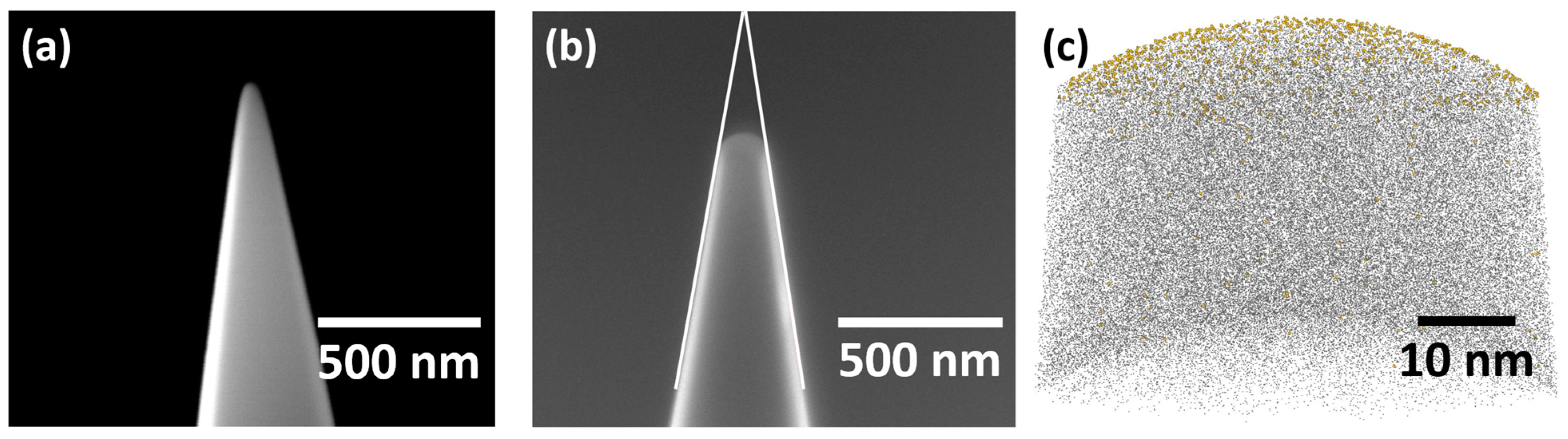
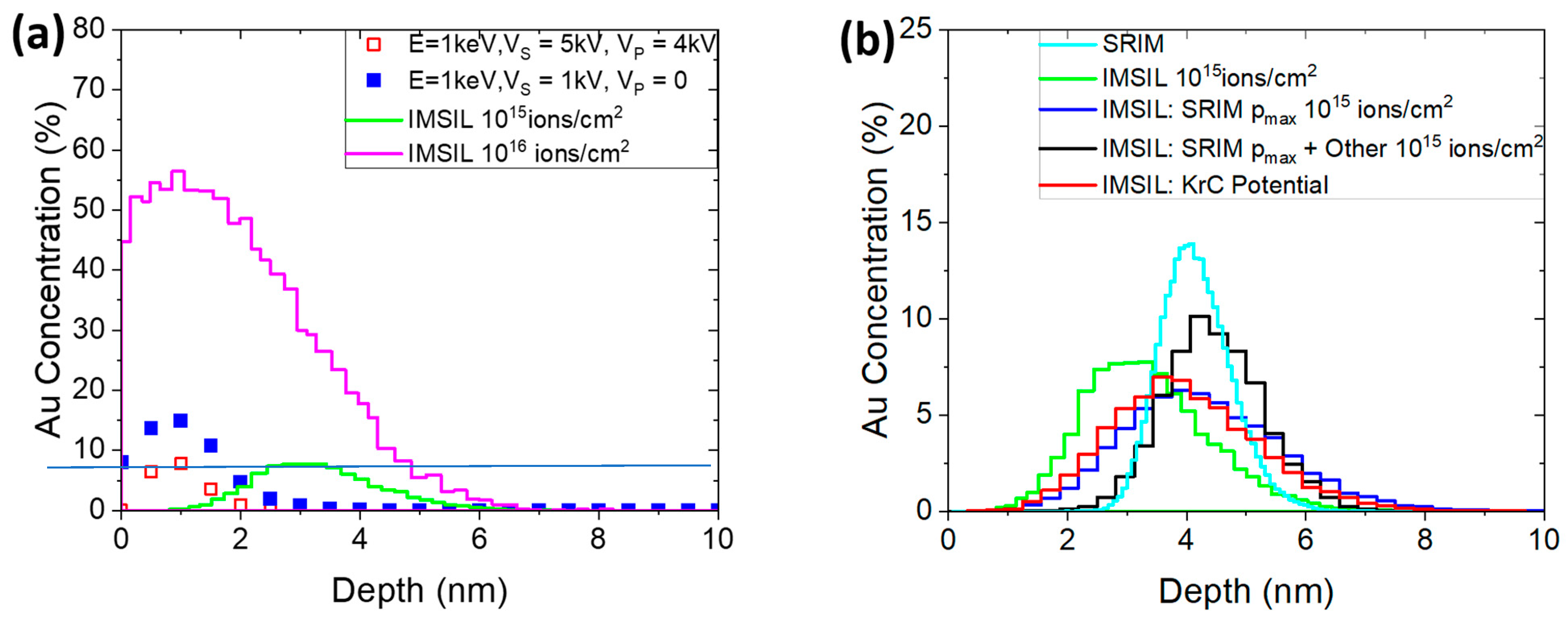
3. Results
4. Discussion
5. Conclusions
Author Contributions
Funding
Data Availability Statement
Acknowledgments
Conflicts of Interest
References
- Williams, J.S. Ion implantation of semiconductors. Mater. Sci. Eng. A 1998, 253, 8–15. [Google Scholar] [CrossRef]
- Rimini, E. Ion Implantation: Basics to Device Fabrication; Springer: New York, NY, USA, 1994. [Google Scholar]
- Goorsky, M. Ion Implantation; InTechOpen: London, UK, 2012. [Google Scholar]
- Palmetshofer, L. Ion implantation in IV–VI semiconductors. Appl. Phy. A 1984, 34, 139–153. [Google Scholar]
- Current, M.I. The role of ion implantation in CMOS scaling: A tutorial review. AIP Conf. Proc. 2019, 2160, 020001. [Google Scholar] [CrossRef]
- Murray, R.; Haynes, K.; Zhao, X.; Perry, S.; Hatem, C.; Jones, K. The effect of low energy ion implantation on MoS2. ECS J. Solid State Sci. Tech. 2016, 5, Q3050. [Google Scholar] [CrossRef]
- Ortolland, C.; Sahhaf, S.; Srividya, V.; Degraeve, R.; Saino, K.; Kim, C.S.; Gilbert, M.; Kauerauf, T.; Cho, M.J.; Dehan, M.; et al. Ion-implantation-based low-cost Hk/MG process for CMOS low-power application. In Proceedings of the 2010 Symposium on VLSI Technology, Honolulu, HI, USA, 15–17 June 2010. [Google Scholar]
- Current, M.I. Perspectives on low-energy ion (and neutral) implantation. In Proceedings of the 2017 17th International Workshop on Junction Technology (IWJT), Uji, Japan, 1–2 June 2017. [Google Scholar]
- Titze, M.; Perry, D.L.; Auden, E.A.; Pacheco, J.L.; Abraham, J.B.S.; Bielejec, E.S. Lithium source for focused ion beam implantation and analysis. J. Vac. Sci. Technol. B 2021, 39, 012802. [Google Scholar] [CrossRef]
- Ebadi, R.; Marshall, M.C.; Phillips, D.F.; Cremer, J.; Zhou, T.; Titze, M.; Kehayias, P.; Saleh Ziabari, M.; Delegan, N.; Rajendran, S.; et al. Directional detection of dark matter using solid-state quantum sensing. AVS Quantum Sci. 2022, 4, 044701. [Google Scholar] [CrossRef]
- Xu, X.; Martin, Z.O.; Titze, M.; Wang, Y.; Sychev, D.; Henshaw, J.; Lagutchev, A.S.; Htoon, H.; Bielejec, E.S.; Bogdanov, S.I.; et al. Fabrication of single color centers in sub-50 nm nanodiamonds using ion implantation. Nanophotonics 2023, 12, 485–494. [Google Scholar] [CrossRef]
- Chandrasekaran, V.; Titze, M.; Flores, A.R.; Campbell, D.; Henshaw, J.; Jones, A.C.; Bielejec, E.S.; Htoon, H. High-Yield Deterministic Focused Ion Beam Implantation of Quantum Defects Enabled by In Situ Photoluminescence Feedback. Adv. Sci. 2023, 10, 2300190. [Google Scholar] [CrossRef]
- Wang, X.; Zimmermann, C.; Titze, M.; Niaouris, V.; Hansen, E.R.; D’Ambrosia, S.H.; Vines, L.; Bielejec, E.S.; Fu, K.-M.C. Properties of Donor Qubits in ZnO Formed by Indium-Ion Implantation. Phys. Rev. Appl. 2023, 19, 054090. [Google Scholar] [CrossRef]
- Sutula, M.; Christen, I.; Bersin, E.; Walsh, M.P.; Chen, K.C.; Mallek, J.; Melville, A.; Titze, M.; Bielejec, E.S.; Hamilton, S.; et al. Large-scale optical characterization of solid-state quantum emitters. Nat. Mater. 2023, 1–7. [Google Scholar] [CrossRef]
- Delegan, N.; Whiteley, S.J.; Zhou, T.; Bayliss, S.L.; Titze, M.; Bielejec, E.; Holt, M.V.; Awschalom, D.D.; Heremans, F.J. Deterministic nanoscale quantum spin-defect implantation and diffraction strain imaging. Nanotechnology 2023, 34, 385001. [Google Scholar] [CrossRef] [PubMed]
- Kang, S.; Jang, W.-S.; Morozovska, A.N.; Kwon, O.; Jin, Y.; Kim, Y.-H.; Bae, H.; Wang, C.; Yang, S.-H.; Belianinov, A. Highly enhanced ferroelectricity in HfO2-based ferroelectric thin film by light ion bombardment. Science 2022, 376, 731–738. [Google Scholar] [CrossRef] [PubMed]
- Stanford, M.G.; Pudasaini, P.R.; Belianinov, A.; Cross, N.; Noh, J.H.; Koehler, M.R.; Mandrus, D.G.; Duscher, G.; Rondinone, A.J.; Ivanov, I.N. Focused helium-ion beam irradiation effects on electrical transport properties of few-layer WSe2: Enabling nanoscale direct write homo-junctions. Sci. Rep. 2016, 6, 27276. [Google Scholar] [CrossRef] [PubMed]
- Sipahigil, A.; Evans, R.E.; Sukachev, D.D.; Burek, M.J.; Borregaard, J.; Bhaskar, M.K.; Nguyen, C.T.; Pacheco, J.L.; Atikian, H.A.; Meuwly, C.; et al. An integrated diamond nanophotonics platform for quantum-optical networks. Science 2016, 354, 847–850. [Google Scholar] [CrossRef]
- Wan, N.H.; Lu, T.-J.; Chen, K.C.; Walsh, M.P.; Trusheim, M.E.; De Santis, L.; Bersin, E.A.; Harris, I.B.; Mouradian, S.L.; Christen, I.R.; et al. Large-scale integration of artificial atoms in hybrid photonic circuits. Nature 2020, 583, 226–231. [Google Scholar] [CrossRef]
- Titze, M.; Byeon, H.; Flores, A.; Henshaw, J.; Harris, C.T.; Mounce, A.M.; Bielejec, E.S. In situ ion counting for improved implanted ion error rate and silicon vacancy yield uncertainty. Nano Lett. 2022, 22, 3212–3218. [Google Scholar] [CrossRef]
- Pak, D.; Nandi, A.; Titze, M.; Bielejec, E.S.; Alaeian, H.; Hosseini, M. Long-range cooperative resonances in rare-earth ion arrays inside photonic resonators. Commun. Phys. 2022, 5, 89. [Google Scholar] [CrossRef]
- Qian, C.X.; Wang, M.Z.; Lu, S.S.; Feng, H.J. Fabrication of 2D perovskite (PMA) 2PbI4 crystal and Cu ion implantation improved x-ray detector. Appl. Phys. Lett. 2022, 120, 011901. [Google Scholar] [CrossRef]
- Giannazzo, F.; Panasci, S.E.; Schilirò, E.; Fiorenza, P.; Greco, G.; Roccaforte, F.; Cannas, M.; Agnello, S.; Koos, A.; Pécz, B.; et al. Highly Homogeneous 2D/3D Heterojunction Diodes by Pulsed Laser Deposition of MoS2 on Ion Implantation Doped 4H-SiC. Advan. Mater. Inter. 2023, 10, 2201502. [Google Scholar] [CrossRef]
- Fiedler, H.; Gupta, P.; Leveneur, J.; Mitchell, D.R.; Nancarrow, M.; Kennedy, J. Formation of buried 2D Aluminium Gallium Nitride structures with enhanced piezoelectric modulus by xenon ion implantation. Appl. Mater. Today 2023, 30, 101710. [Google Scholar] [CrossRef]
- Xu, K.; Zhao, Y.; Lin, Z.; Long, Y.; Wang, Y.; Chan, M.; Chai, Y. Doping of two-dimensional MoS2 by high energy ion implantation. Sem. Sci. Tech. 2017, 32, 124002. [Google Scholar] [CrossRef]
- Lin, P.-C.; Villarreal, R.; Achilli, S.; Bana, H.; Nair, M.N.; Tejeda, A.; Verguts, K.; De Gendt, S.; Auge, M.; Hofsäss, H.; et al. Doping Graphene with Substitutional Mn. ACS Nano 2021, 15, 5449–5458. [Google Scholar] [CrossRef] [PubMed]
- Lin, Y.-C.; Liu, C.; Yu, Y.; Zarkadoula, E.; Yoon, M.; Puretzky, A.A.; Liang, L.; Kong, X.; Gu, Y.; Strasser, A.; et al. Low Energy Implantation into Transition-Metal Dichalcogenide Monolayers to Form Janus Structures. ACS Nano 2020, 14, 3896–3906. [Google Scholar] [CrossRef] [PubMed]
- Evans, R.E.; Bhaskar, M.K.; Sukachev, D.D.; Nguyen, C.T.; Sipahigil, A.; Burek, M.J.; Machielse, B.; Zhang, G.H.; Zibrov, A.S.; Bielejec, E.; et al. Photon-mediated interactions between quantum emitters in a diamond nanocavity. Science 2018, 362, 662–665. [Google Scholar] [CrossRef]
- Meesala, S.; Sohn, Y.-I.; Pingault, B.; Shao, L.; Atikian, H.A.; Holzgrafe, J.; Gündoğan, M.; Stavrakas, C.; Sipahigil, A.; Chia, C.; et al. Strain engineering of the silicon-vacancy center in diamond. Phys. Rev. B 2018, 97, 205444. [Google Scholar] [CrossRef]
- Belianinov, A.; Burch, M.J.; Ievlev, A.; Kim, S.; Stanford, M.G.; Mahady, K.; Lewis, B.B.; Fowlkes, J.D.; Rack, P.D.; Ovchinnikova, O.S. Direct write of 3D nanoscale mesh objects with platinum precursor via focused helium ion beam induced deposition. Micromachines 2020, 11, 527. [Google Scholar] [CrossRef]
- Bischoff, L.; Mazarov, P.; Bruchhaus, L.; Gierak, J. Liquid metal alloy ion sources—An alternative for focussed ion beam technology. Appl. Phys. Rev. 2016, 3, 021101. [Google Scholar] [CrossRef]
- Bui, M.N.; Rost, S.; Auge, M.; Tu, J.-S.; Zhou, L.; Aguilera, I.; Blügel, S.; Ghorbani-Asl, M.; Krasheninnikov, A.V.; Hashemi, A.; et al. Low-energy Se ion implantation in MoS2 monolayers. npj 2D Mater. Appl. 2022, 6, 42. [Google Scholar] [CrossRef]
- Bui, M.N.; Rost, S.; Auge, M.; Zhou, L.; Friedrich, C.; Blügel, S.; Kretschmer, S.; Krasheninnikov, A.V.; Watanabe, K.; Taniguchi, T.; et al. Optical Properties of MoSe2 Monolayer Implanted with Ultra-Low-Energy Cr Ions. ACS Appl. Mater. Interfaces 2023, 15, 35321–35331. [Google Scholar] [CrossRef]
- Ziegler, J.F. Stopping and Range of Ions in Matter (SRIM). Available online: www.srim.org (accessed on 17 February 2023).
- Titze, M.; Pacheco, J.L.; Byers, T.; Van Deusen, S.B.; Perry, D.L.; Weathers, D.; Bielejec, E.S. Evaluation of the accuracy of stopping and range of ions in matter simulations through secondary ion mass spectrometry and Rutherford backscattering spectrometry for low energy heavy ion implantation. J. Vac. Sci. Technol. A 2021, 39, 063222. [Google Scholar] [CrossRef]
- Weber, W.J.; Zhang, Y. Predicting damage production in monoatomic and multi-elemental targets using stopping and range of ions in matter code: Challenges and recommendations. Curr. Opin. Solid State Mater. Sci. 2019, 23, 100757. [Google Scholar] [CrossRef]
- Wittmaack, K. Misconceptions impairing the validity of the stopping power tables in the SRIM library and suggestions for doing better in the future. Nucl. Instrum. Methods Phys. Res. Sect. B Beam Interact. Mater. At. 2016, 380, 57–70. [Google Scholar] [CrossRef]
- Hofsäss, H.; Zhang, K.; Mutzke, A. Simulation of ion beam sputtering with SDTrimSP, TRIDYN and SRIM. Appl. Surf. Sci. 2014, 310, 134–141. [Google Scholar] [CrossRef]
- Shulga, V.I. Note on the artefacts in SRIM simulation of sputtering. Appl. Surf. Sci. 2018, 439, 456–461. [Google Scholar] [CrossRef]
- Biersack, J.P.; Eckstein, W. Sputtering studies with the Monte Carlo Program TRIM.SP. Appl. Phys. A 1984, 34, 73–94. [Google Scholar] [CrossRef]
- Hofsäss, H.; Junge, F.; Kirscht, P.; van Stiphout, K. Low energy ion-solid interactions: A quantitative experimental verification of binary collision approximation simulations. Mater. Res. Express 2023, 10, 075003. [Google Scholar] [CrossRef]
- Möller, W.; Eckstein, W. Tridyn—A TRIM simulation code including dynamic composition changes. Nucl. Instrum. Methods Phys. Res. Sect. B Beam Interact. Mater. At. 1984, 2, 814–818. [Google Scholar] [CrossRef]
- Hobler, G. Monte Carlo simulation of two-dimensional implanted dopant distributions at mask edges. Nucl. Instrum. Methods Phys. Res. Sect. B Beam Interact. Mater. At. 1995, 96, 155–162. [Google Scholar] [CrossRef]
- Hobler, G.; Maciążek, D.; Postawa, Z. Ion bombardment induced atom redistribution in amorphous targets: MD versus BCA. Nucl. Instrum. Methods Phys. Res. Sect. B Beam Interact. Mater. At. 2019, 447, 30–33. [Google Scholar] [CrossRef]
- Hobler, G.; Simionescu, A. Acceleration of binary collision simulations in crystalline targets using critical angles for ion channeling. Nucl. Instrum. Methods Phys. Res. Sect. B Beam Interact. Mater. At. 1995, 102, 24–28. [Google Scholar] [CrossRef]
- Lai, H.; McJunkin, T.R.; Miller, C.J.; Scott, J.R.; Almirall, J.R. The predictive power of SIMION/SDS simulation software for modeling ion mobility spectrometry instruments. Int. J. Mass Spectrom. 2008, 276, 1–8. [Google Scholar] [CrossRef]
- Kreissig, U.; Kahn, A.; Ruedenauer, F.G.; Steiger, W. Mass and energy analyses of an AuSi liquid metal ion source. J. Phys. D Appl. Phys. 1990, 23, 959. [Google Scholar] [CrossRef]
- Ziegler, J.F.; Manoyan, J.M. The stopping of ions in compounds. Nucl. Instrum. Methods Phys. Res. Sect. B Beam Interact. Mater. At. 1988, 35, 215–228. [Google Scholar] [CrossRef]
- Lindhard, J.; Scharff, M. Energy Dissipation by Ions in the kev Region. Phys. Rev. 1961, 124, 128–130. [Google Scholar] [CrossRef]
- Oen, S.O.; Robinson, T.M. Computer studies of the reflection of light ions from solids. Nucl. Instrum. Methods 1976, 132, 647–653. [Google Scholar] [CrossRef]
- Eckstein, W. Sputtering. In Computer Simulation of Ion-Solid Interactions; Eckstein, W., Ed.; Springer: Berlin/Heidelberg, Germany, 1991; pp. 169–218. [Google Scholar]


| VS | VP | Energy | Fluence | Measured | SRIM | TRIDYN | IMSIL | ||||
|---|---|---|---|---|---|---|---|---|---|---|---|
| Depth | Straggle | Depth | Straggle | Depth | Straggle | Depth | Straggle | ||||
| kV | kV | keV | ions/cm2 | nm | |||||||
| 1 | 0 | 1 | 1016 | 0.86 | 0.76 | 4.10 | 0.58 | 4.95 | 1.60 | 1.51 | 1.58 |
| 5 | 4 | 1 | 1015 | 0.71 | 0.62 | 5.49 | 1.03 | 3.20 | 1.00 | ||
Disclaimer/Publisher’s Note: The statements, opinions and data contained in all publications are solely those of the individual author(s) and contributor(s) and not of MDPI and/or the editor(s). MDPI and/or the editor(s) disclaim responsibility for any injury to people or property resulting from any ideas, methods, instructions or products referred to in the content. |
© 2023 by the authors. Licensee MDPI, Basel, Switzerland. This article is an open access article distributed under the terms and conditions of the Creative Commons Attribution (CC BY) license (https://creativecommons.org/licenses/by/4.0/).
Share and Cite
Titze, M.; Poplawsky, J.D.; Kretschmer, S.; Krasheninnikov, A.V.; Doyle, B.L.; Bielejec, E.S.; Hobler, G.; Belianinov, A. Measurement and Simulation of Ultra-Low-Energy Ion–Solid Interaction Dynamics. Micromachines 2023, 14, 1884. https://doi.org/10.3390/mi14101884
Titze M, Poplawsky JD, Kretschmer S, Krasheninnikov AV, Doyle BL, Bielejec ES, Hobler G, Belianinov A. Measurement and Simulation of Ultra-Low-Energy Ion–Solid Interaction Dynamics. Micromachines. 2023; 14(10):1884. https://doi.org/10.3390/mi14101884
Chicago/Turabian StyleTitze, Michael, Jonathan D. Poplawsky, Silvan Kretschmer, Arkady V. Krasheninnikov, Barney L. Doyle, Edward S. Bielejec, Gerhard Hobler, and Alex Belianinov. 2023. "Measurement and Simulation of Ultra-Low-Energy Ion–Solid Interaction Dynamics" Micromachines 14, no. 10: 1884. https://doi.org/10.3390/mi14101884
APA StyleTitze, M., Poplawsky, J. D., Kretschmer, S., Krasheninnikov, A. V., Doyle, B. L., Bielejec, E. S., Hobler, G., & Belianinov, A. (2023). Measurement and Simulation of Ultra-Low-Energy Ion–Solid Interaction Dynamics. Micromachines, 14(10), 1884. https://doi.org/10.3390/mi14101884