
Optimization AlGaN/GaN HEMT with Field Plate Structures


Abstract
:1. Introduction
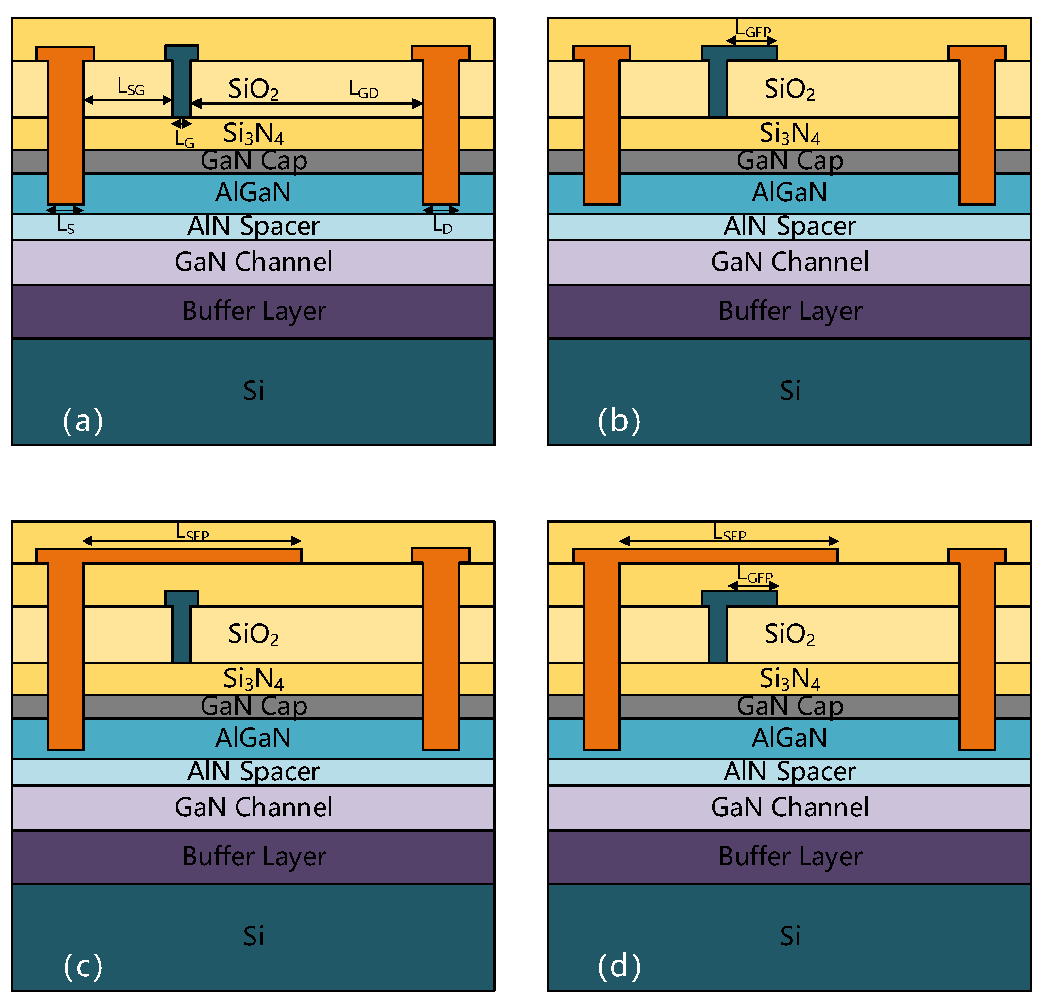
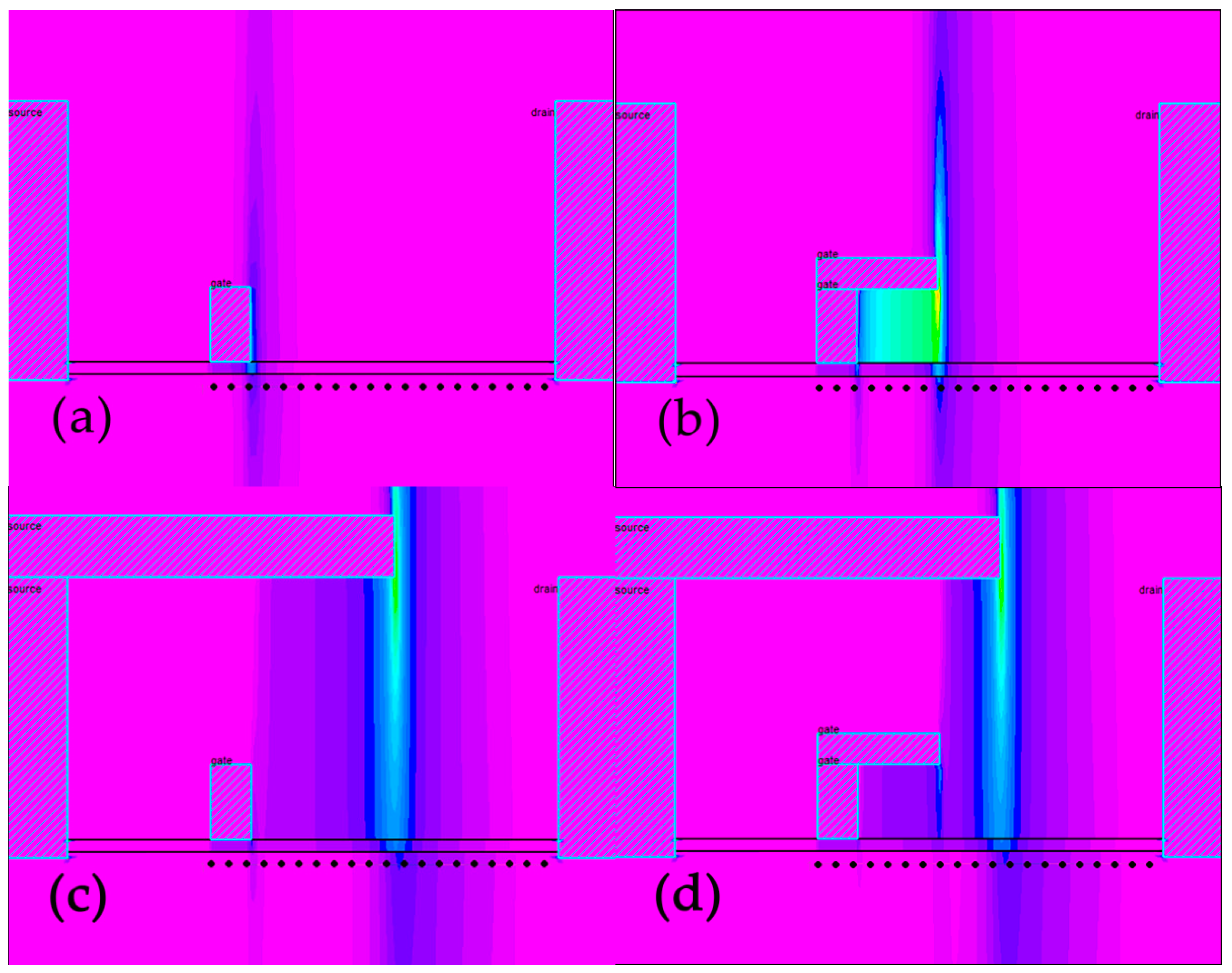
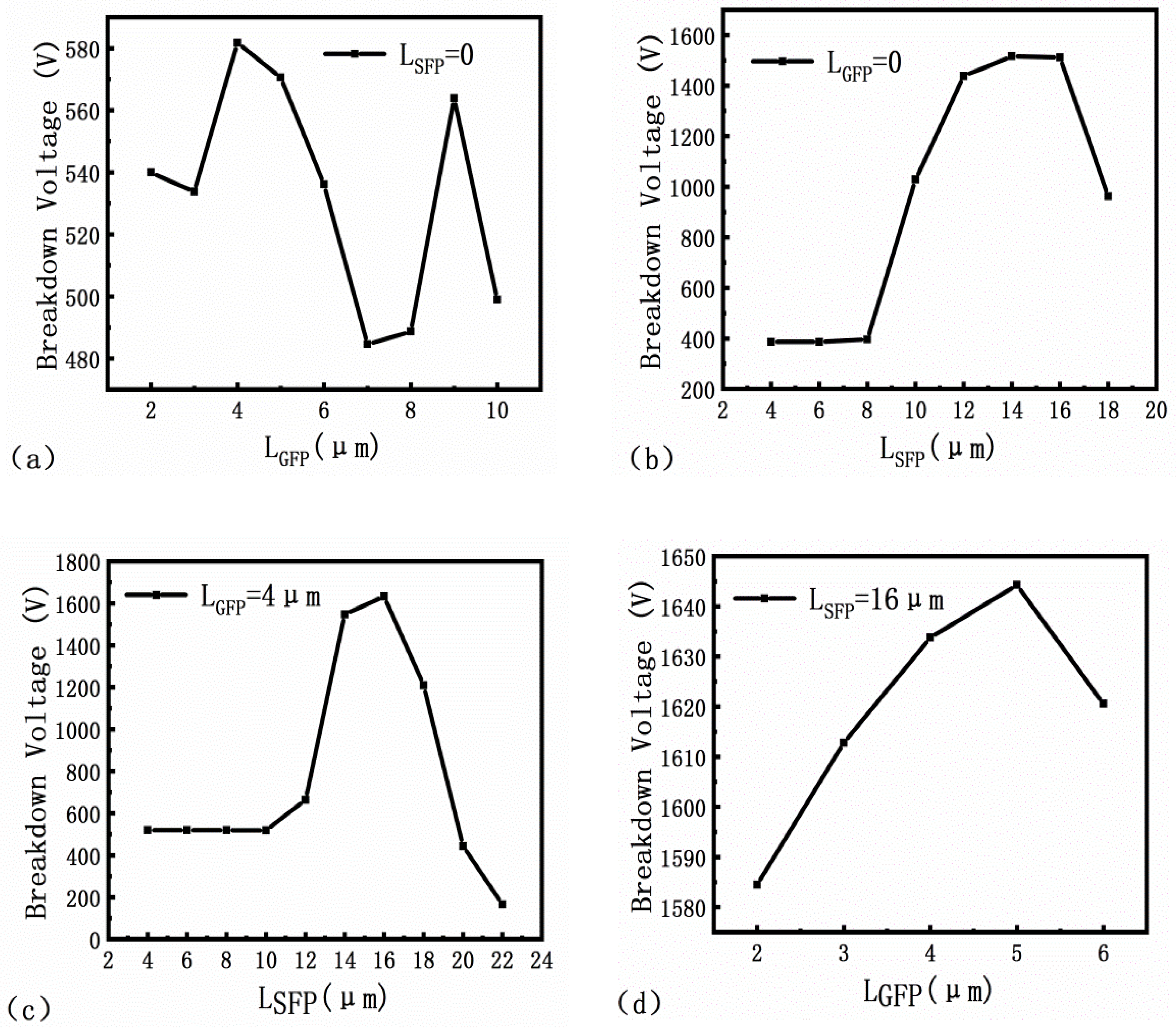
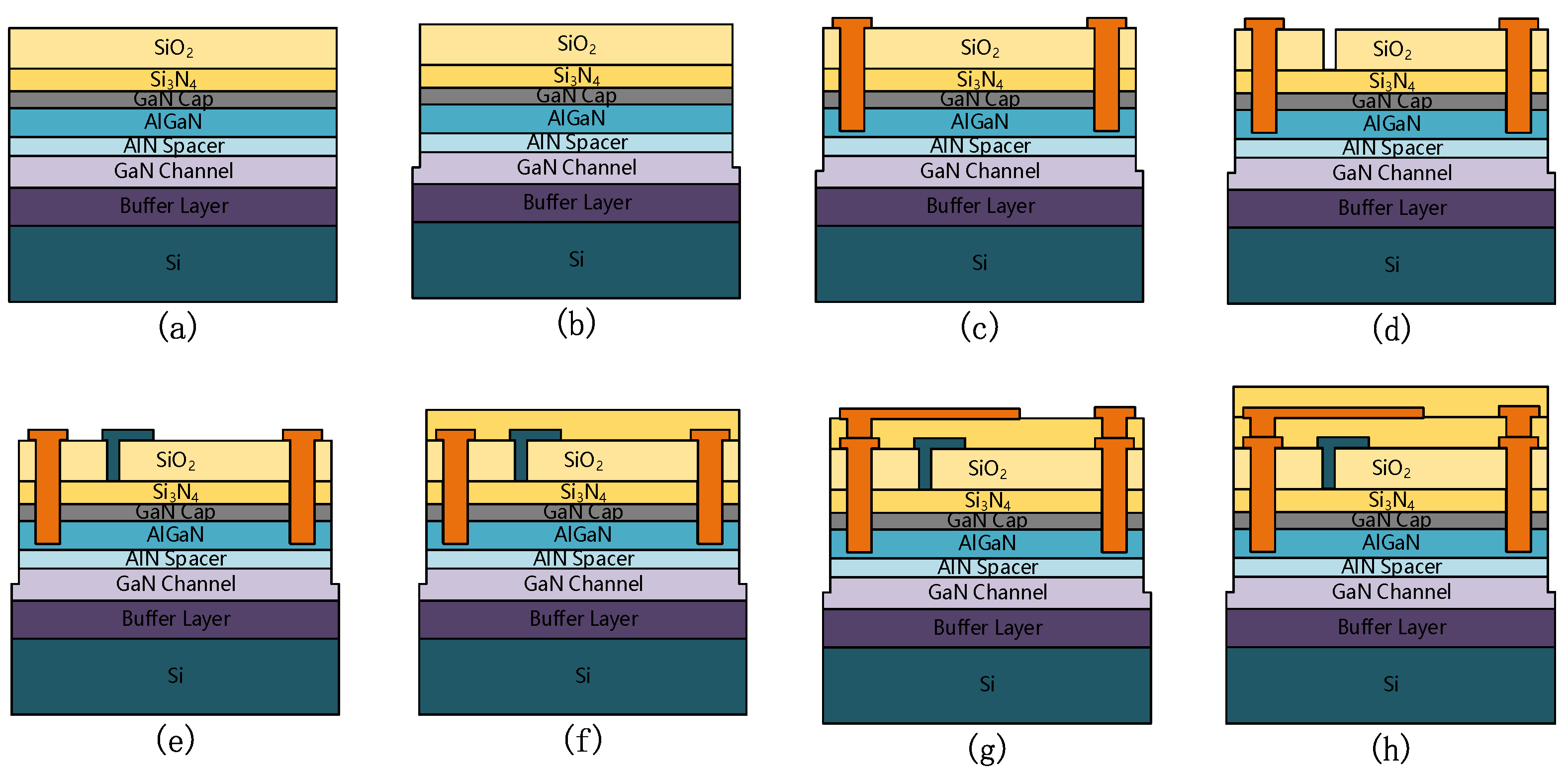
2. Device Design and Simulation Model
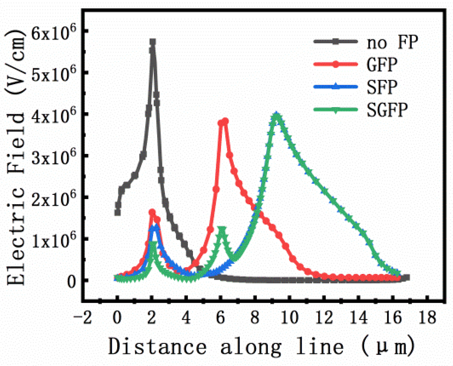
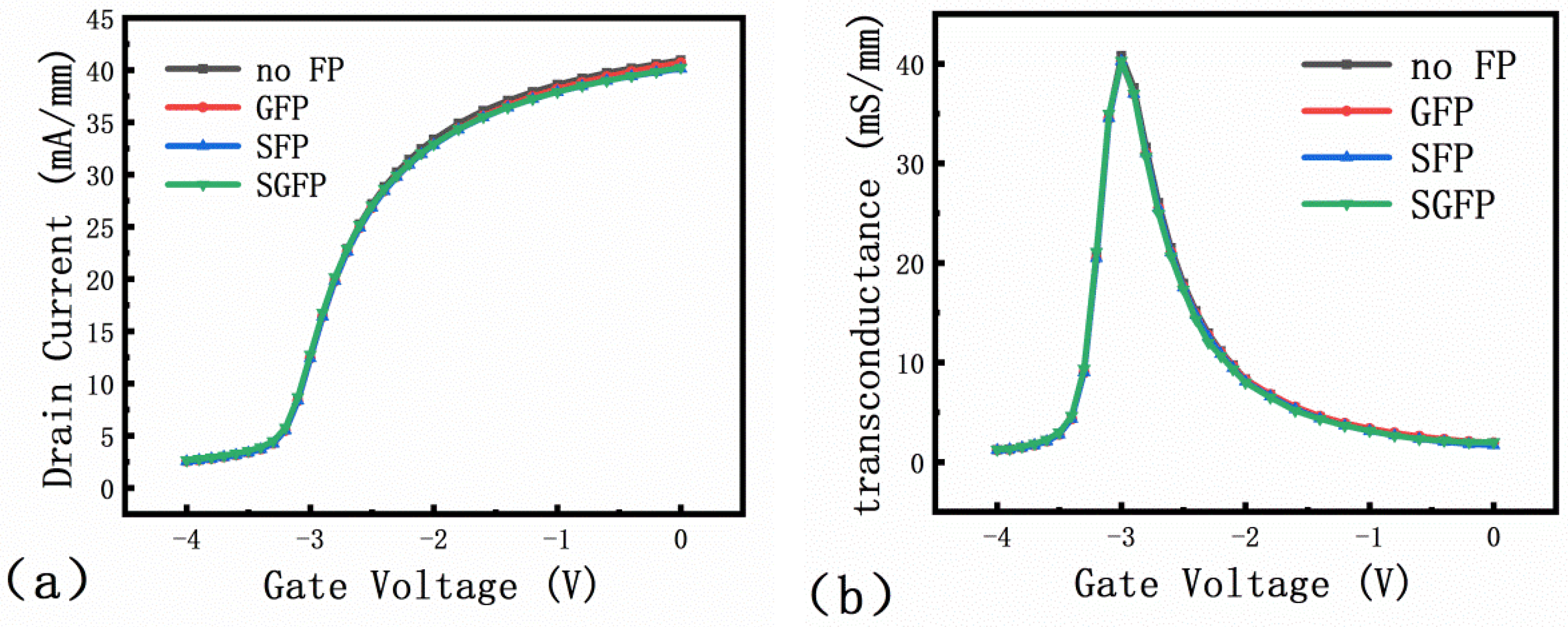
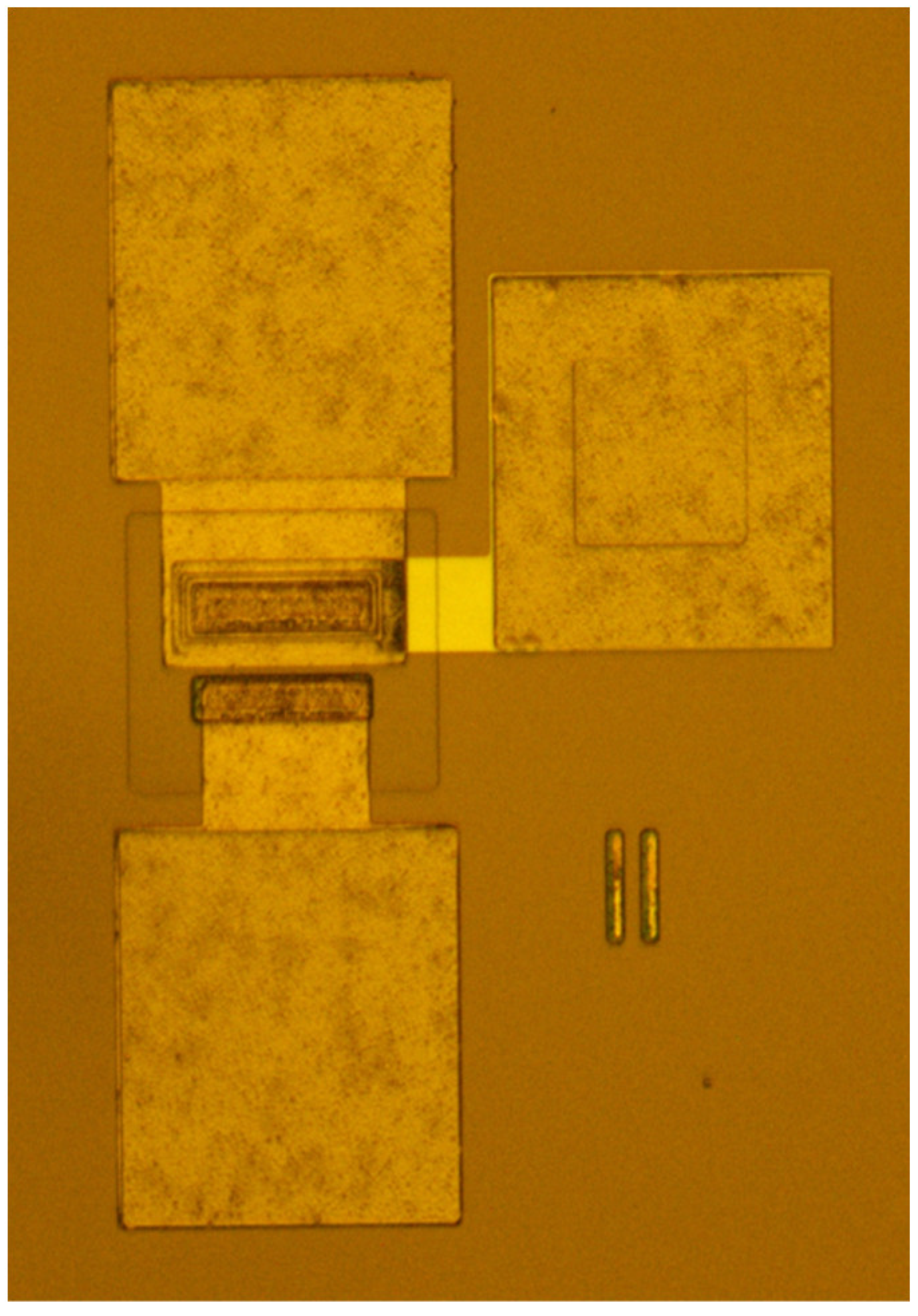
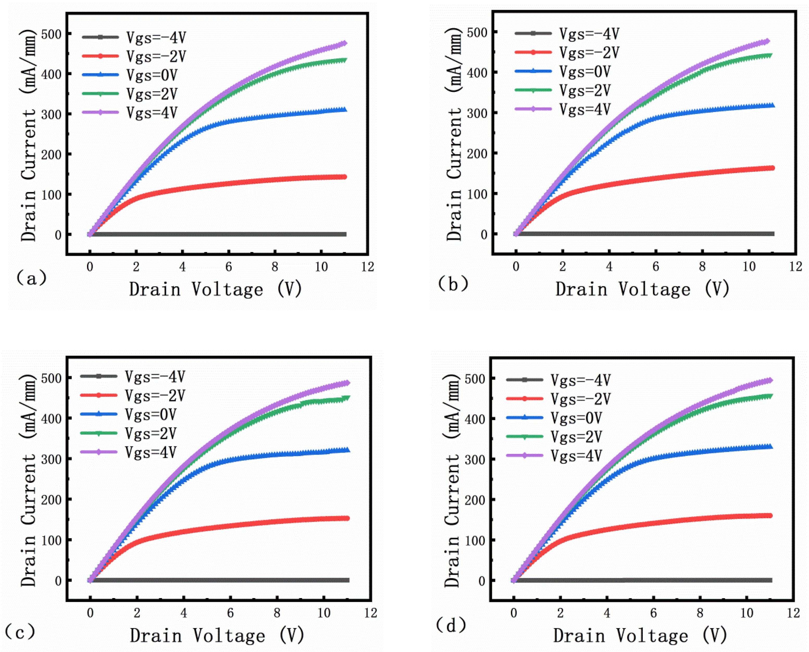
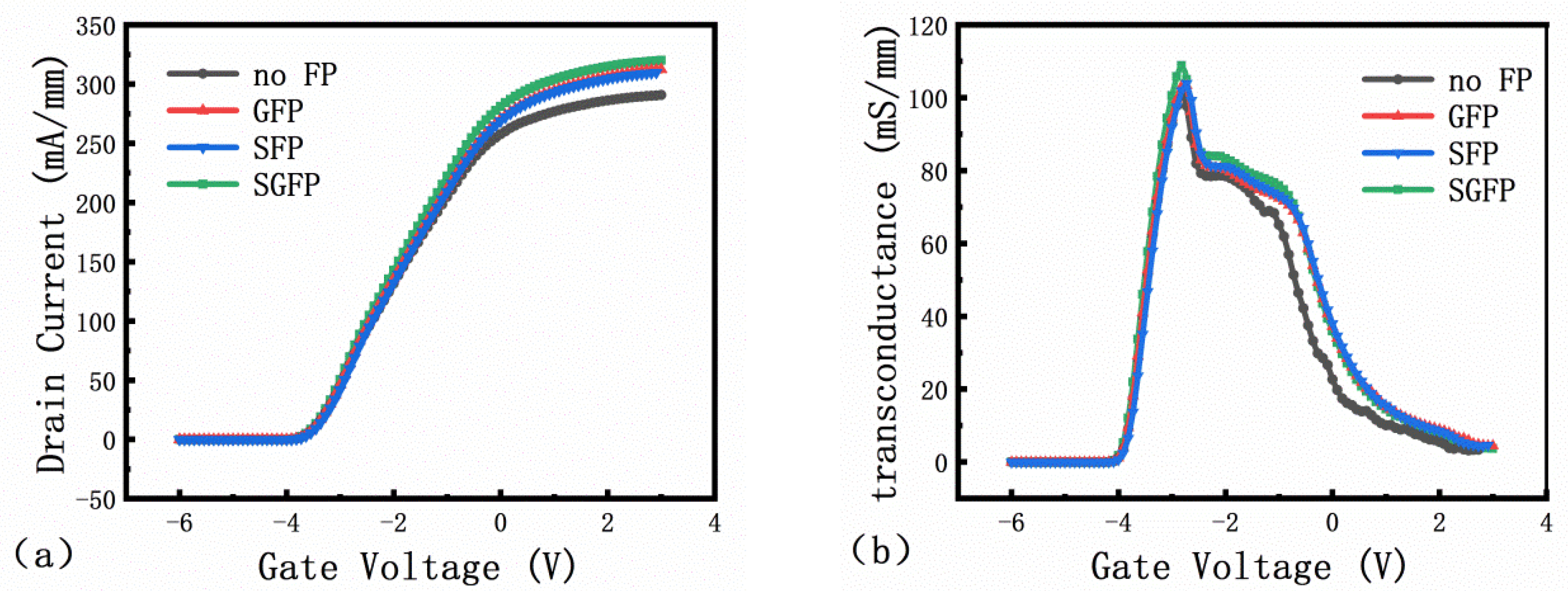
3. Experimental Results and Tests
4. Conclusions
Author Contributions
Funding
Data Availability Statement
Conflicts of Interest
References
- He, J.; Cheng, W.C.; Wang, Q.; Cheng, K.; Yu, H.; Chai, Y. Recent Advances in GaN-Based Power HEMT Devices. Adv. Electron Mater. 2021, 7, 2001045. [Google Scholar] [CrossRef]
- Kumar, V.; Kumar, S.; Maan, A.S.; Akhtar, J. Interfacial and structural analysis of MeV heavy ion irradiated SiC. Appl. Nanosci. 2021, 1–8. [Google Scholar] [CrossRef]
- Tierney, B.D.; Choi, S.; Dasgupta, S.; Dickerson, J.R.; Reza, S.; Kaplar, R.J.; Baca, A.G.; Marinella, M.J. Evaluation of a “Field Cage” for Electric Field Control in GaN-Based HEMTs That Extends the Scalability of Breakdown Into the kV Regime. IEEE Trans. Electron Devices 2017, 64, 3740–3747. [Google Scholar] [CrossRef]
- Lu, B.; Palacios, T. High Breakdown (>1500) AlGaN/GaN HEMTs by Substrate-Transfer Technology. IEEE Electron Device Lett. 2010, 31, 951–953. [Google Scholar] [CrossRef]
- Wu, Y.; Jacob-Mitos, M.; Moore, M.L.; Heikman, S. A 97.8% Efficient GaN HEMT Boost Converter With 300-W Output Power at 1 MHz. IEEE Electron Device Lett. 2008, 29, 824–826. [Google Scholar] [CrossRef]
- Das, J.; Everts, J.; van den Keybus, J.; van Hove, M.; Visalli, D.; Srivastava, P.; Marcon, D.; Cheng, K.; Leys, M.; Decoutere, S.; et al. A 96% Efficient High-Frequency DC–DC Converter Using E-Mode GaN DHFETs on Si. IEEE Electron Device Lett. 2011, 32, 1370–1372. [Google Scholar] [CrossRef] [Green Version]
- Saito, W.; Kakiuchi, Y.; Nitta, T.; Saito, Y.; Noda, T.; Fujimoto, H.; Yoshioka, A.; Ohno, T.; Yamaguchi, M. Field-Plate Structure Dependence of Current Collapse Phenomena in High-Voltage GaN-HEMTs. IEEE Electron Device Lett. 2010, 31, 659–661. [Google Scholar] [CrossRef]
- Hemanth, A.; Reddy, M.K.; Lakshmi, J.; Kumar, B.H.; Bandi, L.; Sheu, G.; Song, Y.-L.; Chen, P.-A.; Chang, L.-M. Investigations of low dynamic ron on GaN/AlGaN/GaN HEMT by field plate using physical device simulations. In Proceedings of the 2019 6th International Conference on Systems and Informatics (ICSAI), Shanghai, China, 2–4 November 2019; IEEE: Manhattan, NY, USA, 2019; pp. 249–252. [Google Scholar]
- Godfrey, D.; Nirmal, D.; Arivazhagan, L.; Roy, B.; Chen, Y.-L.; Yu, T.-H.; Yeh, W.-K.; Godwinraj, D. Investigation of AlGaN/GaN HEMT Breakdown analysis with Source field plate length for High power applications. In Proceedings of the 2020 5th International Conference on Devices, Circuits and Systems (ICDCS), Coimbatore, India, 5–6 March 2020; IEEE: Manhattan, NY, USA, 2020; pp. 244–246. [Google Scholar]
- Wang, L.D.; Wang, Z.J.; Cheng, X.H.; Wan, L. The characteristics of gate-source double field-plates for GaN HEMT. J. Funct. Mater. Devices 2014, 6, 1007–4252. [Google Scholar]
- Hu, Q.; Zeng, F.; Cheng, W.-C.; Zhou, G.; Wang, Q.; Yu, H. Reducing dynamic on-resistance of p-GaN gate HEMTs using dual field plate configurations. In Proceedings of the 2020 IEEE International Symposium on the Physical and Failure Analysis of Integrated Circuits (IPFA), Singapore, 20–23 July 2020; IEEE: Manhattan, NY, USA, 2020; pp. 1–4. [Google Scholar]
- Karmalkar, S.; Mishra, U.K. Enhancement of breakdown voltage in AlGaN/GaN high electron mobility transistors using a field plate. IEEE Trans. Electron Devices 2001, 48, 1515–1521. [Google Scholar] [CrossRef]
- Quay, R.J.S.S. Technology, Gallium Nitride Electronics; Springer Science & Business Media: Berlin/Heidelberg, Germany, 2013; Volume 28, p. 70301. [Google Scholar]
- Saito, W.; Takada, Y.; Kuraguchi, M.; Tsuda, K.; Omura, I.; Ogura, T. Design and demonstration of high breakdown voltage GaN high electron mobility transistor (HEMT) using field plate structure for power electronics applications. Jpn. J. Appl. Phys. 2004, 43, 2239. [Google Scholar] [CrossRef]
- Wang, H.; Shi, Y.; Xin, Y.; Liu, C.; Lu, G.; Huang, Y.J.M. Improving Breakdown Voltage and Threshold Voltage Stability by Clamping Channel Potential for Short-Channel Power p-GaN HEMTs. Micromachines 2022, 13, 176. [Google Scholar] [CrossRef] [PubMed]
- Li, W.; Wang, Q.; Zhan, X.; Yan, J.; Jiang, L.; Yin, H.; Gong, J.; Wang, X.; Liu, F.; Li, B.; et al. Impact of dual field plates on drain current degradation in InAlN/AlN/GaN HEMTs. Semicond. Sci. Technol. 2016, 31, 125003. [Google Scholar] [CrossRef]
- Xing, H.; Dora, Y.; Chini, A.; Heikman, S.; Keller, S.; Mishra, U.K. High Breakdown Voltage AlGaN–GaN HEMTs Achieved by Multiple Field Plates. IEEE Electron Device Lett. 2004, 25, 161–163. [Google Scholar] [CrossRef] [Green Version]
- Neha; Kumari, V.; Gupta, M.; Saxena, M. TCAD-Based Optimization of Field Plate Length & Passivation Layer of AlGaN/GaN HEMT for Higher Cut-Off Frequency & Breakdown Voltage. IETE Tech. Rev. 2020, 1–9. [Google Scholar] [CrossRef]
- Murugapandiyan, P.; Nirmal, D.; Ajayan, J.; Varghese, A.; Ramkumar, N.J.S. Investigation of influence of SiN and SiO2 passivation in gate field plate double heterojunction Al0.3Ga0.7N/GaN/Al0.04Ga0.96N high electron mobility transistors. Silicon 2022, 14, 1421–1429. [Google Scholar] [CrossRef]
- Das, P.; Lenka, T.; Mahato, S.S.; Panda, A. Source/drain, gate and channel engineering in HEMTs. In Handbook for III–V High Electron Mobility Transistor Technologies; CRC Press: Boca Raton, FL, USA, 2019; pp. 81–95. [Google Scholar]


| Parameters | GaN | AlGaN |
|---|---|---|
| Eg300 (eV) | 3.4 | 3.96 |
| Align | 0.8 | 0.8 |
| Permittivity | 9.5 | 9.5 |
| Saturation Velocity (Vsatn) | 1.9 × 107 cm/s | 1.1 × 107 cm/s |
| Electron Low Field Mobility (Mun) | 900 cm2/Vs | 600 cm2/Vs |
| Hole Low Field Mobility (Mup) | 10 cm2/Vs | 10 cm2/Vs |
| 300K conduction band state density (Nc300) | 2.24 × 1018 cm3 | 2.07 × 1018 cm3 |
| 300K valance band state density (Nv300) | 1.16 × 1019 cm3 | 1.16 × 1019 cm3 |
| No FP | G-FP | S-FP | SG-FP | |
|---|---|---|---|---|
| Ids (mA/mm) | 476 | 477.1 | 487 | 494.7 |
| Vth (V) | −3.9 | −3.9 | −3.9 | −3.9 |
| gm(mS/mm) | 100.7 | 102 | 103.2 | 108.9 |
| VBV (V) | 312 | 860 | 1041 | 1118 |
| Ron (Ω) | 9.9 | 9.8 | 9.7 | 9.2 |
| Ron.sp (mΩ•cm2) | 2.67 | 2.65 | 2.62 | 2.48 |
| FOM (MW•cm2) | 36.5 | 279.1 | 413.6 | 504 |
Publisher’s Note: MDPI stays neutral with regard to jurisdictional claims in published maps and institutional affiliations. |
© 2022 by the authors. Licensee MDPI, Basel, Switzerland. This article is an open access article distributed under the terms and conditions of the Creative Commons Attribution (CC BY) license (https://creativecommons.org/licenses/by/4.0/).
Share and Cite
Shi, N.; Wang, K.; Zhou, B.; Weng, J.; Cheng, Z. Optimization AlGaN/GaN HEMT with Field Plate Structures. Micromachines 2022, 13, 702. https://doi.org/10.3390/mi13050702
Shi N, Wang K, Zhou B, Weng J, Cheng Z. Optimization AlGaN/GaN HEMT with Field Plate Structures. Micromachines. 2022; 13(5):702. https://doi.org/10.3390/mi13050702
Chicago/Turabian StyleShi, Ningping, Kejia Wang, Bing Zhou, Jiafu Weng, and Zhiyuan Cheng. 2022. "Optimization AlGaN/GaN HEMT with Field Plate Structures" Micromachines 13, no. 5: 702. https://doi.org/10.3390/mi13050702
APA StyleShi, N., Wang, K., Zhou, B., Weng, J., & Cheng, Z. (2022). Optimization AlGaN/GaN HEMT with Field Plate Structures. Micromachines, 13(5), 702. https://doi.org/10.3390/mi13050702