Article

Novel Step Floating Islands VDMOS with Low Specific on-Resistance by TCAD Simulation

1
Beijing Engineering Research Center of High-Reliability IC with Power Industrial Grade, Beijing Smart-Chip Microelectronics Technology Co., Ltd., Beijing 102299, China
2
Beijing Chip Identification Technology Co., Ltd., Beijing 102299, China
3
Key Laboratory of the Ministry of Education for Wide Band-Gap Semiconductor Materials and Devices, School of Microelectronics, Xidian University, No. 2 South TaiBai Road, Xi’an 710071, China
*
Author to whom correspondence should be addressed.
Micromachines 2022, 13(4), 573; https://doi.org/10.3390/mi13040573
Submission received: 8 March 2022 / Revised: 24 March 2022 / Accepted: 29 March 2022 / Published: 4 April 2022

Abstract

:
A novel VDMOS with Step Floating Islands VDMOS (S-FLI VDMOS) is proposed for the first time in this letter, in order to optimize the breakdown voltage (BV) and the specific on-resistance (Ron,sp). The innovative terminal technology of Breakdown Point Transfer (BPT) is applied to S-FLI VDMOS, which transfers the breakdown point from the high electric field region to the low electric field region, and the S-FLI VDMOS structure uses multiple layers of charge compensation blocks to generate multiple electric field peaks in the drift region in order to optimize the electric field distribution. In the TCAD simulation, the BV of the proposed S-FLI VDMOS is improved to 326 V, which is higher than that of 281 V for the conventional Si VDMOS with the same drift region length of 15 μm, and the Ron,sp is reduced from 21.54 mΩ·cm2 for the conventional Si VDMOS to 7.77 mΩ·cm2 for the S-FLI VDMOS. Compared with the conventional Si VDMOS, the current density of the effective current conduction path is increased when the forward bias is applied to the proposed device.

1. Introduction

Vertical Double-diffusion Metal Oxide Semiconductor (VDMOS) is an important component in the field of power semiconductor devices and has been widely used due to its high switching speed, low loss, and high breakdown voltage (BV) [1]. However, the main problem with VDMOS power devices is that specific on-resistance (Ron,sp) increases sharply with the increasing BV, which greatly limits the development and application of VDMOS power devices. In order to alleviate the contradictory relationship between the Ron,sp and BV, several new structures have been proposed to reduce the Ron,sp of the drift region, including superjunction (SJ) VDMOS, floating island MOSFET (FLIMOS) etc. [2,3,4,5,6,7,8,9,10]. However, the manufacturing process of SJ VDMOS is difficult and requires a strict charge balance. When the device is turned on, the P-type impurity compensation layer of SJ VDMOS occupies the conduction channel of the device [4].
In order to break the contradiction between the Ron,sp and BV of traditional Si devices, a novel VDMOS with Step Floating Islands VDMOS (S-FLI VDMOS) is proposed for the first time in this letter (seen Figure 1). The structure uses multiple layers of charge compensation blocks to generate multiple electric field peaks in the drift region, optimizing the electric field distribution. Compared with the conventional Si VDMOS, the BV is significantly improved, and the Ron,sp is effectively reduced. At the same time, the charge compensation region quickly shifts from the P-type base to the substrate, and when the forward bias is applied, the effective current conduction path of the device is increased. With the same BV, the Ron,sp of S-FLI VDMOS is smaller than that of FLIMOS [11,12,13,14]. The assisted depletion effect and electric field modulation can be applied in the lower-voltage devices to decrease the Ron,sp and higher-voltage devices to improve the BV, respectively.

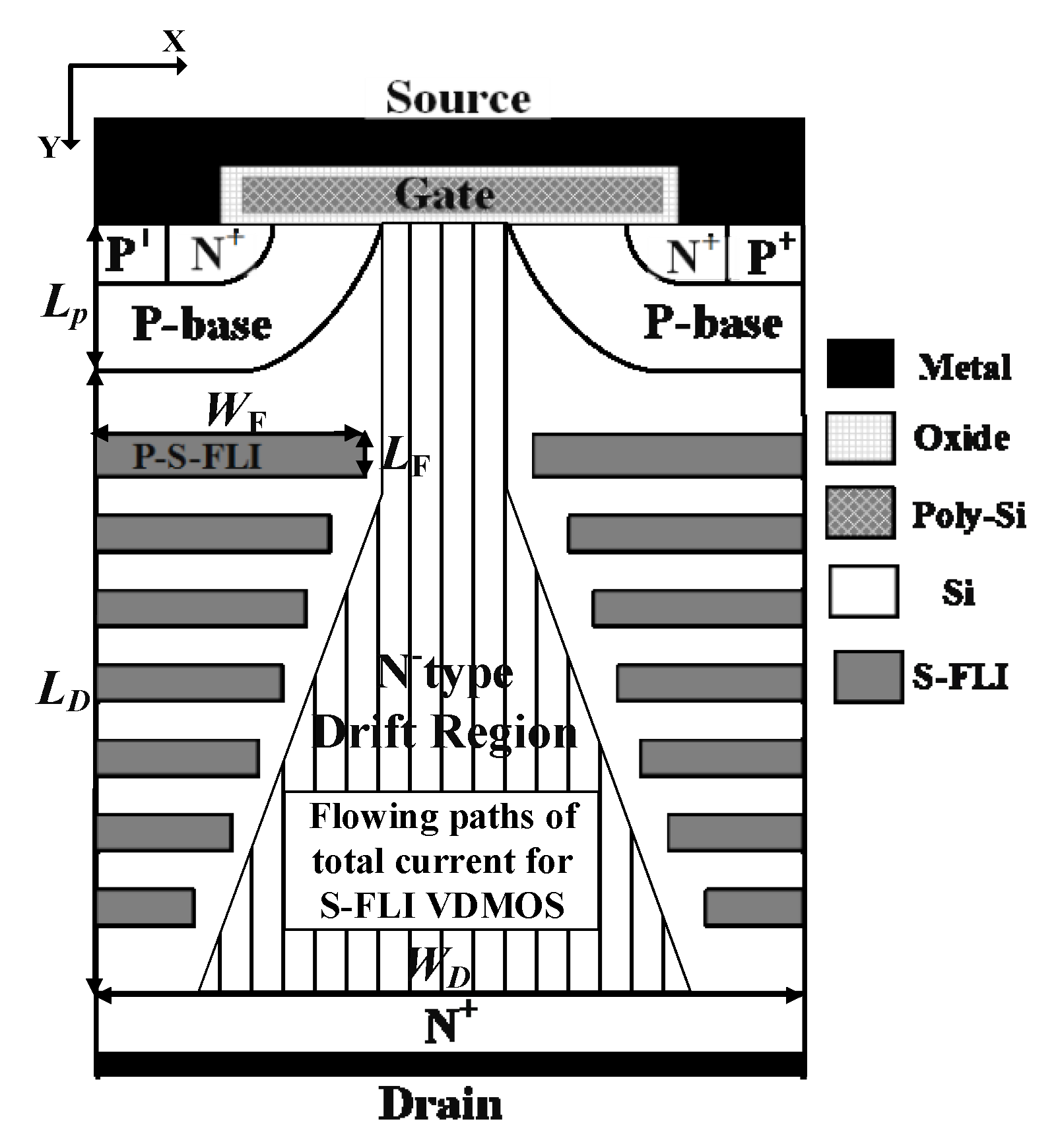
2. Device Structure and Description

The novel VDMOS with Step Floating Islands VDMOS (S-FLI VDMOS) is proposed. Figure 1 shows a cell of the proposed S-FLI VDMOS. The key feature is the Step Floating Islands [11,12,13,14] which consists of multiple P-type layers of charge compensation blocks in the N-type drift region. Two Step Floating Islands at the same Y coordinate in Figure 1 constituted a ring. The key steps of one feasible fabrication method for the proposed S-FLI VDMOS are shown below. First, the epitaxial growth N-Si Layer on the N+ Si Sub, and boron ions implantation and thermal diffusion form the P-type Floating Island. Next, the epitaxial growth N-Si Layer and boron ions implantation to form the second P-type Floating Island with a width slightly shorter than that of the first layer. This continues until seven Floating Islands are formed. Then, the thin gate oxide is employed with a typical thickness of 400 Å after a thermal growth process, and the source region is formed by phosphorus and boron ions implantation, respectively. Finally, a thick oxide passivation layer is deposited, and source, gate, and drain electrodes are formed. The electric field peaks are introduced to optimize the electric field distribution due to Step Floating Islands. Furthermore, S-FLI VDMOS exhibits better performance when the number of rings is increased. For the proposed S-FLI VDMOS, with the reverse drain voltage further increased, the electric field at area B (shown in Figure 2b) will reach the critical electric field of the Si material. The breakdown point will be transferred from area A (shown in Figure 2a) for the conventional Si VDMOS to area B for the S-FLI VDMOS by Breakdown Point Transfer (BPT).
The environment temperature is 300 K. BV is obtained at VGS = 0 V, and Ron,sp is obtained at VGS = 10 V. The physics models applied in the ISE simulation mainly includes Mobility (DopingDep High Field Sat Enormal), EffectiveIntrinsic Density (OldSlotboom), Recombination (SRH (DopingDep) and Auger Avalanche (Eparal)). The criterion of breakdown is BreakCriteria {Current (Contact = “drain” Absval = 1e−7)}. The breakdown condition is defined as the point at which the ionization integral equals unity. It is necessary to optimize the parameters in the numerical simulations. Some device parameters in the simulation are listed in Table 1. The simulation results based on the parameters in Table 1 are shown in Table 2.

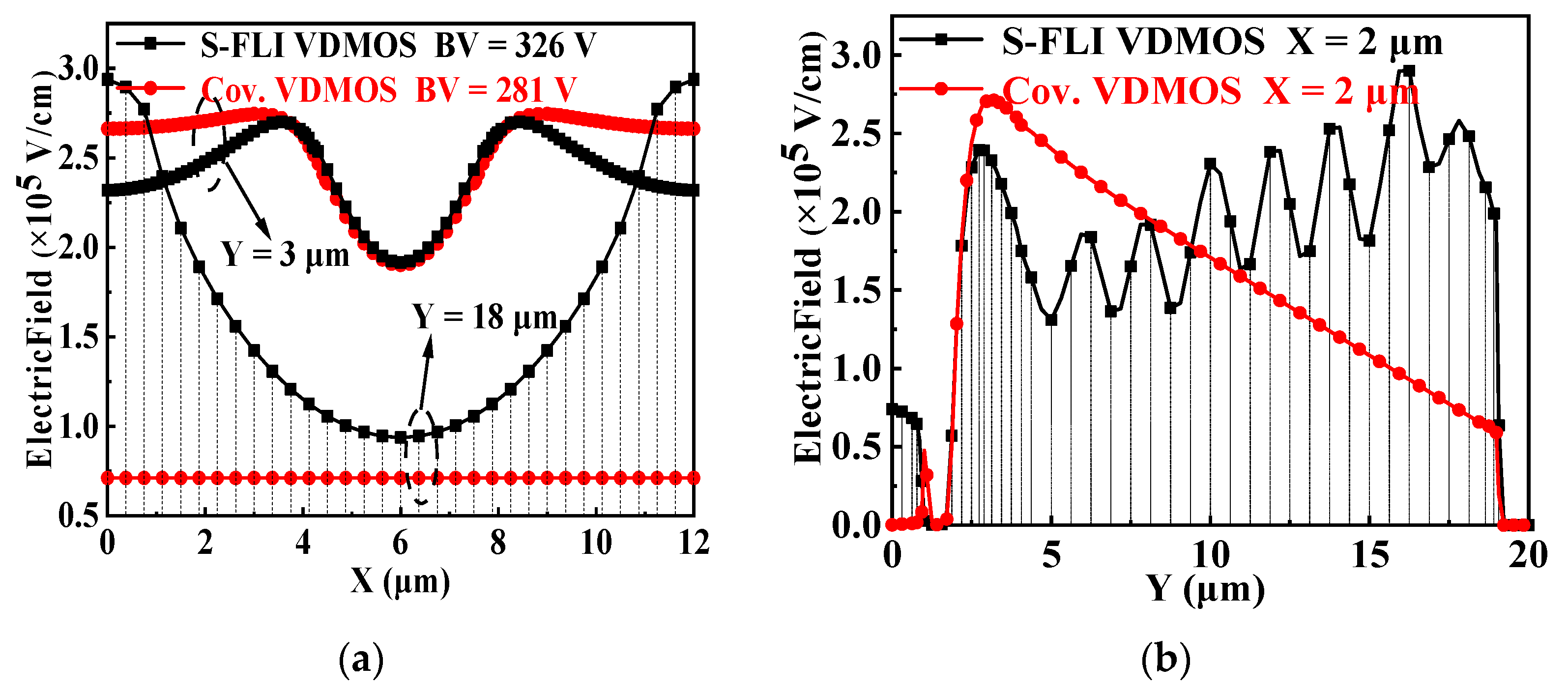
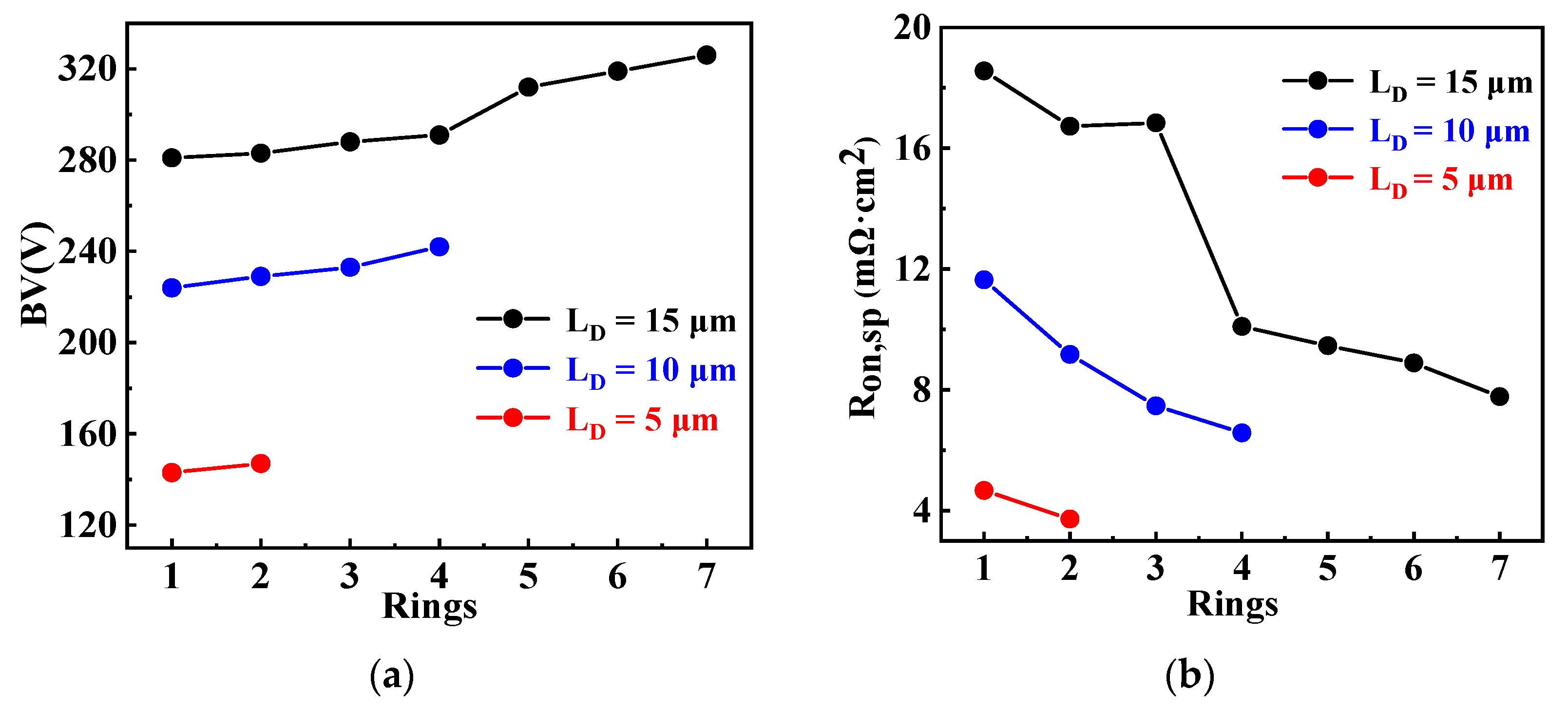
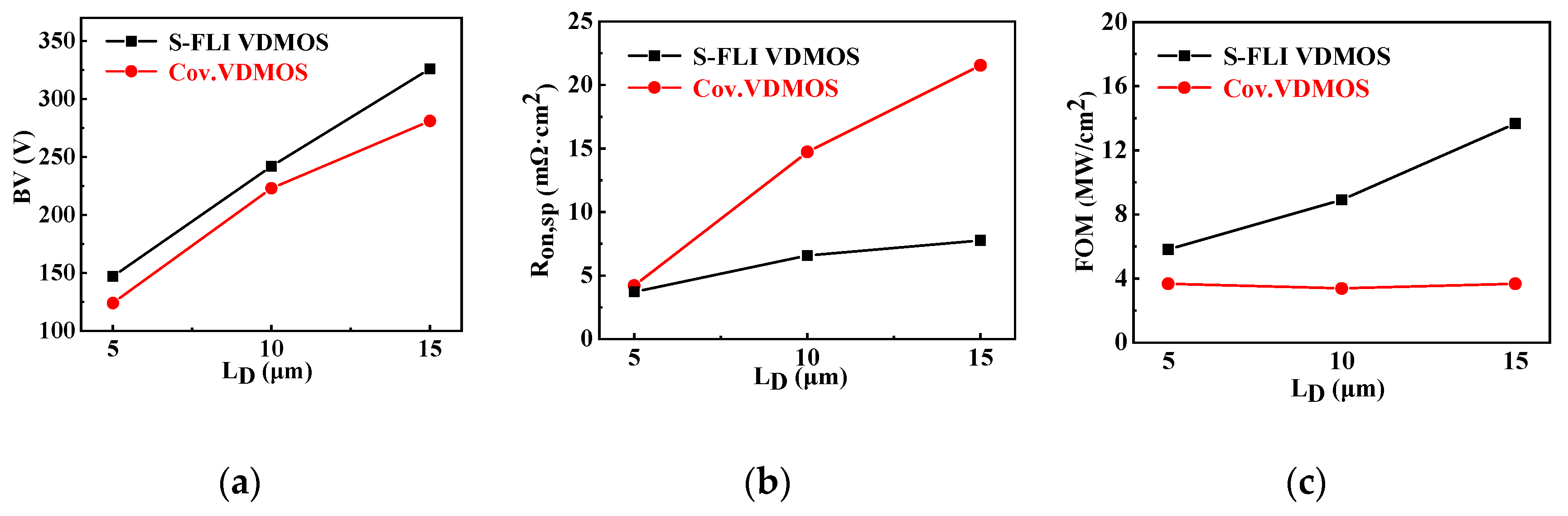
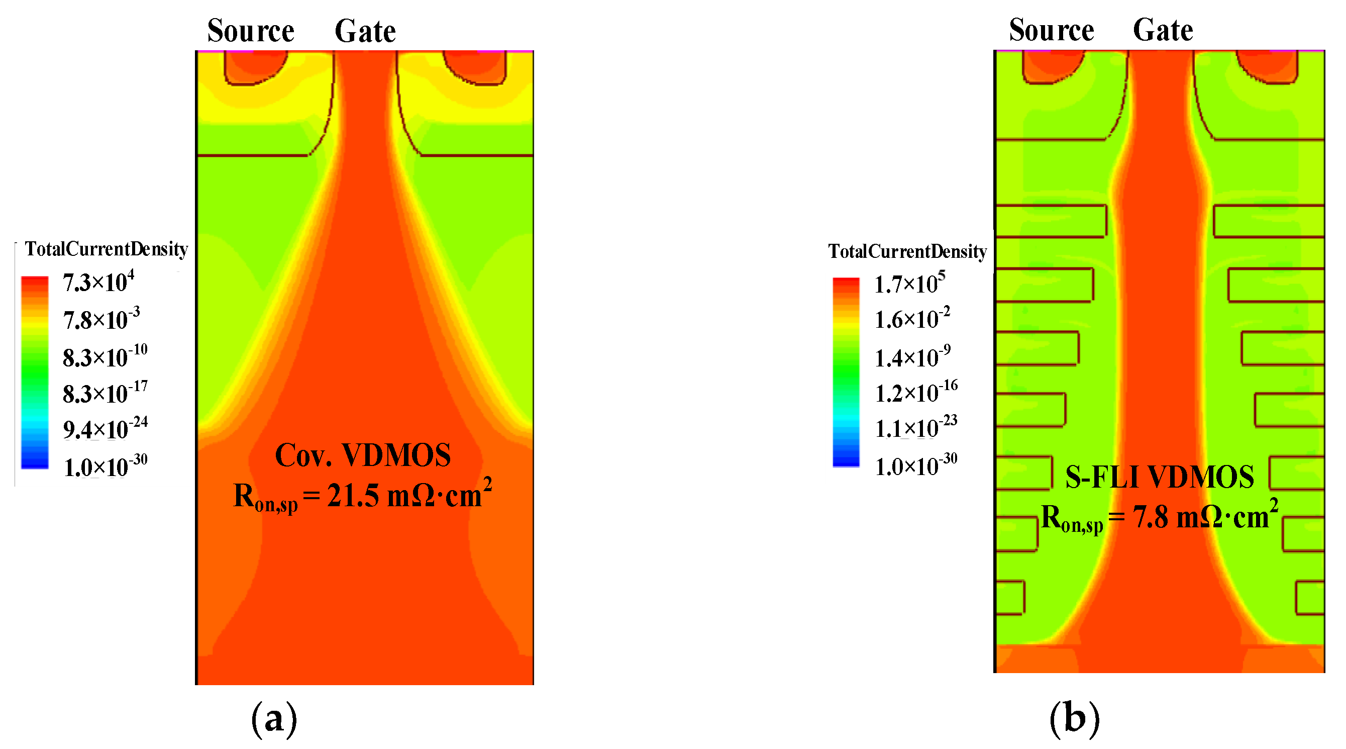
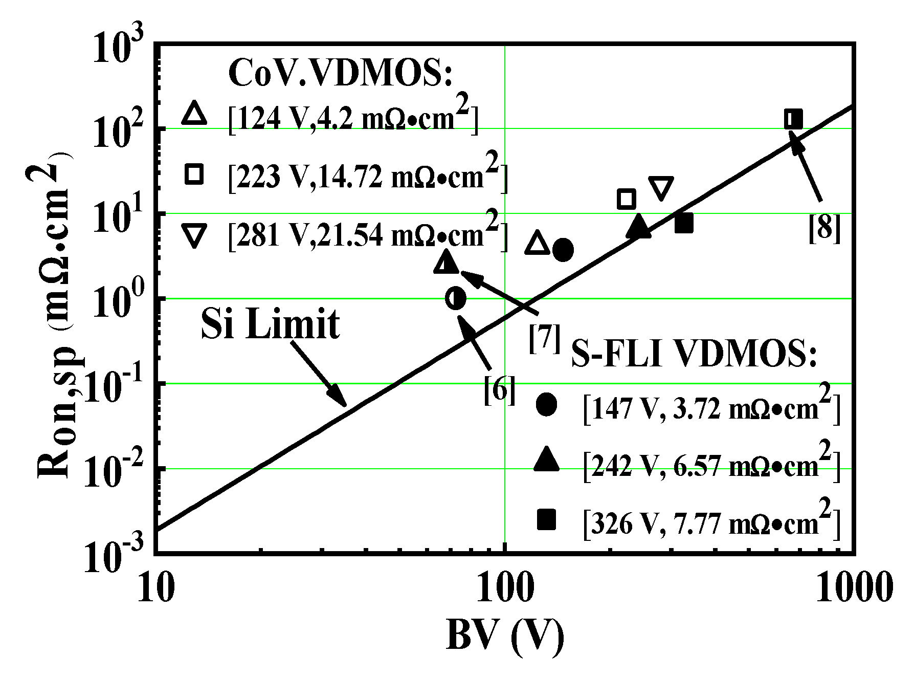
3. Results and Discussion

The lateral electric fields and vertical electric fields distributions are shown in Figure 3a,b for the conventional Si VDMOS and S-FLI VDMOS, respectively. Figure 3a presents the lateral electric fields of the two devices at Y = 3 μm and Y = 18 μm. The electric field of the S-FLI VDMOS is higher compared with the conventional Si VDMOS, due to the multiple P-type layers of charge compensation blocks in the N-type drift region. However, the vertical electric fields of the conventional Si VDMOS and S-FLI VDMOS are different. For the conventional Si VDMOS, the highest electric field occurs at the junction of the P base and N-type drift region, resulting in a low BV of 281 V. For S-FLI VDMOS, as can be seen from Figure 3b, the peak electric field at the edge of drain has been introduced to the area B, and the vertical electric field distribution is extremely improved due to the electrical modulation of seven new electric field peaks introduced by Step Floating Islands. In addition, the auxiliary junctions created by multiple P-type layers of charge compensation blocks jointly sustain a high BV (326 V) for S-FLI VDMOS, which is improved by 16% compared to the conventional Si VDMOS (281 V) with the same LD.
Figure 4 shows the dependence of BV and Ron,sp on LD and the Rings for S-FLI VDMOS. It can be seen that the BV is improved and the Ron,sp is decreased with increasing Rings. This is because the new electric field peaks increased due to Step Floating Islands. This caused the Ron,sp to drop from 18.56 mΩ·cm2 to 7.77 mΩ·cm2, and the BV increased from 281 V to 326 V with the number of rings increased at the LD of 15 μm.
The dependence of BV, Ron,sp and Figure-Of-Merit (FOM = BV2/Ron,sp) on LD for the conventional Si VDMOS and S-FLI VDMOS are shown in Figure 5. It is found that the BV of S-FLI VDMOS increases faster and saturates at a longer LD as the LD increases (BV > 300 V, at LD =15 μm). Additionally, the Ron,sp of S-FLI VDMOS is lower than that of the conventional counterpart, yielding a higher FOM (13.68 MW/cm2) of S-FLI VDMOS than that (3.67 MW/cm2) of the conventional one with the same LD of 15 μm.
Figure 6 shows the distribution and flowing paths of total current for the conventional Si VDMOS and S-FLI VDMOS in on-state. Since the P-type S-FLI assists in depleting the N-type drift region in the off-state so that the optimum ND is further increased, the current density for the proposed S-FLI VDMOS is higher compared to conventional Si VDMOS; thus, it is helpful for the Ron,sp.
The output characteristics and transfer characteristics of the conventional Si VDMOS and S-FLI VDMOS are shown in Figure 7. The threshold voltages VTH of the two devices are approximately 5 V. At different gate voltages VGS (5.0, 5.5, 6.0, 10 V), S-FLI VDMOS exhibits better output performance than the conventional counterpart, which leads to the result that the Ron,sp (7.77 mΩ·cm2) of S-FLI VDMOS is lower than that (21.54 mΩ·cm2) of the conventional VDMOS.
Figure 8 shows the Ron,sp versus BV for the S-FLI VDMOS, the conventional Si VDMOS, the reported structure, and the proposed VDMOS [6,7,8]. It can be seen that S-FLI VDMOS exhibits better performance at the BV, which further breaks the silicon limit under the optimized conditions.

4. Conclusions

The novel VDMOS with Step Floating Islands VDMOS (S-FLI VDMOS) is proposed in this letter. The structure uses multiple layers of charge compensation blocks to generate multiple electric field peaks in the drift region and optimize the electric field distribution. The BV (BV = 326 V) is significantly improved, and the Ron,sp (Ron,sp = 7.77 mΩ·cm2) is effectively reduced compared to the conventional Si VDMOS (BV = 281 V, Ron,sp = 21.54 mΩ·cm2) with the same LD of 15 μm. When the forward bias is applied, the current density of the effective current conduction path of the S-FLI VDMOS is increased compared with the conventional Si VDMOS.

Author Contributions

Methodology, B.D. and X.Y.; resources, F.L., X.L. and T.L.; writing—original draft preparation, B.D., X.Y. and M.L.; writing—review and editing, B.D., X.Y. and M.L.; supervision, Y.Y.; project administration, D.Z., Y.W., Y.C., J.S. and Z.F. All authors have read and agreed to the published version of the manuscript.

Funding

This research was funded by The Laboratory Open Fund of Beijing Smart-chip Microelectronics Technology Co., Ltd., grant number SGITZX00XSJ52108591, National Basic Research Program of China, grant number 2015CB351906, Science Foundation for Distinguished Young Scholars of Shaanxi Province, grant number 2018JC-017 and 111 Project, grant number B12026.

Institutional Review Board Statement

Not applicable.

Informed Consent Statement

Not applicable.

Data Availability Statement

Not applicable.

Conflicts of Interest

The authors declare no conflict of interest.

References

  1. Chen, W.Z.; Chen, J.J.; Lin, J.J. Simulation study on the high-k SJ-VDMOS with gradient side-wall. In Proceedings of the 41st International Convention on Information and Communication Technology, Electronics and Microelectronics (MIPRO), Opatija, Croatia, 21–25 May 2018. [Google Scholar]
  2. Williams, R.K.; Darwish, M.N.; Blanchard, R.A.; Siemieniec, R.; Rutter, P.; Kawaguchi, Y. The trench power MOSFET: Part II—Application Specific VDMOS, LDMOS, Packaging, and Reliability. IEEE Trans. Electron Devices 2017, 64, 692–712. [Google Scholar] [CrossRef]
  3. Williams, R.K.; Darwish, M.N.; Blanchard, R.A.; Siemieniec, R.; Rutter, P.; Kawaguchi, Y. The trench power MOSFET: Part I—History, technology, and prospects. IEEE Trans. Electron Devices 2017, 64, 674–691. [Google Scholar] [CrossRef]
  4. Udrea, F.; Deboy, G.; Fujihira, T. Superjunction Power Devices, History, Development, and Future Prospects. IEEE Trans. Electron Devices 2017, 64, 720–734. [Google Scholar] [CrossRef]
  5. Zhou, X.; Feng, Q.; Chen, X. The Study of P-pillar and Trench Technology in VDMOS. In Proceedings of the 2019 PhotonIcs & Electromagnetics Research Symposium-Spring (PIERS-Spring), Rome, Italy, 17–20 June 2019. [Google Scholar]
  6. Chen, Y.; Buddharaju, K.D.; Liang, Y.C.; Samudra, G.S. Superjunction Power LDMOS on Partial SOI Platform. In Proceedings of the 19th International Symposium on Power Semiconductor Devices and ICs, Jeju, Korea, 27–31 May 2007. [Google Scholar]
  7. Tam, W.; Siu, S.; Yang, B.; Kok, C.; Wong, H. Off-state drain breakdown mechanisms of VDMOS with anti-JFET implantation. Microelectron. Reliab. 2011, 51, 2064–2068. [Google Scholar] [CrossRef]
  8. Chen, X.; Feng, Q.; Jin, T. 600-V shielded trench split-gate VDMOS improving the figure of merit. Int. J. Electron. 2019, 107, 1083–1097. [Google Scholar] [CrossRef]
  9. Duan, B.; Wang, Y.; Wang, Y.; Dong, Z.; Yang, Y. Novel Vertical Power MOSFET with Step Hk Insulator Close to Super Junction Limit Relationship between Breakdown Voltage and Specific on-Resistance by Improving Electric Field Modulation. IEEE Trans. Electron Devices 2021, 68, 5048–5054. [Google Scholar] [CrossRef]
  10. Cao, Z.; Duan, B.; Shi, T.; Yuan, S.; Yang, Y. A superjunction U-MOSFET with SIPOS pillar breaking superjunction silicon limit by TCAD simulation study. IEEE Electron Device Lett. 2017, 38, 794–797. [Google Scholar] [CrossRef]
  11. Cezac, N.; Rossel, P.; Morancho, F.; Tranduc, H.; Peyre-Lavigne, A.; Pages, I. A new generation of power devices based on the concept of the “Floating Islands”. In Proceedings of the 22th International Conference on Microelectronics (Cat. No.00TH8400), Nis, Yugoslavia, 14–17 May 2000. [Google Scholar]
  12. Alves, S.; Morancho, F.; Reynes, J.-M.; Margheritta, J.; Deram, I.; Isoird, K.; Tranduc, H. Technological realization of low on-resistance FLYMOS/spl trade/transistors dedicated to automotive applications. In Proceedings of the European Conference on Power Electronics and Applications, Dresden, Germany, 11–14 September 2005. [Google Scholar]
  13. Vaid, R.; Padha, N. Factors Limiting the Device Performance in Power FLIMOSFET: 2-D Simulation Study. In Proceedings of the International Conference on Electrical Engineering, Lahore, Pakistan, 11–12 April 2007. [Google Scholar]
  14. Vaid, R.; Padha, N. Numerical Analysis of a Trench Gate FLIMOSFET with No Quasi-Saturation, Improved Specific on Resistance and Better Synchronous Rectifying Characteristics. In Proceedings of the 25th International Conference on Microelectronics, Belgrade, Serbia, 14–17 May 2006. [Google Scholar]
Figure 1. Cross section of S-FLI VDMOS with the number of rings of 7. Two Step Floating Islands at the same Y coordinate constitute a ring. (LD is the length of N-drift region. LP is the depth of the P-base. WD is the width of device. LF is the depth of Floating Islands. WF is the length of Floating Islands. ND is the concentration of N-drift region. NSUB is the concentration of P-substrate. NP is the concentration of P-base region. Rings is the number of rings, in which two Step Floating Islands at the same Y coordinate constitute a ring.).
Micromachines 13 00573 g001
Figure 2. Distributions of the leakage current, (a) Cov.VDMOS, (b) S-FLI VDMOS.
Micromachines 13 00573 g002
Figure 3. (a) Lateral electric field distributions for the conventional Si VDMOS and S-FLI VDMOS with Rings of 7: Y = 3 μm, Y = 18 μm and (b) Vertical electric field distributions for the conventional Si VDMOS and S-FLI VDMOS with Rings of 7: X = 2 μm.
Micromachines 13 00573 g003
Figure 4. Dependences of (a) BV and (b) Ron,sp on Rings values and LD for S-FLI VDMOS.
Micromachines 13 00573 g004
Figure 5. Dependences of (a) BV, (b) Ron,sp and (c) figure-of-merit (FOM) on LD for the conventional Si VDMOS and S-FLI VDMOS.
Micromachines 13 00573 g005
Figure 6. The distribution and flowing paths of total current for the (a) conventional Si VDMOS and (b) S-FLI VDMOS in on-state.
Micromachines 13 00573 g006
Figure 7. (a) Output characteristics and (b) transfer characteristics of the conventional Si VDMOS and S-FLI VDMOS.
Micromachines 13 00573 g007
Figure 8. The Ron,sp versus BV with the ideal silicon limit, the reported structure and proposed Si VDMOS.
Micromachines 13 00573 g008
Table 1. Device parameters in the simulation.
DeviceCov. VDMOSSJ VDMOSS-FLI VDMOS
LD (μm)151515
Rings//7
ND (cm−3)0.7 × 10153.5 × 10153 × 1015
Np (cm−3)5 × 10175 × 10175 × 1017
NSUB (cm−3)1 × 10141 × 10141 × 1014
LD is the length of N-drift region. ND is the concentration of N-drift region. NSUB is the concentration of P-substrate. NP is the concentration of P-base region. Rings is the number of rings, in which a ring consists of two Step Floating Islands at the same Y coordinate.
Table 2. Simulation results for the Cov. VDMOS, SJ VDMOS and S-FLI VDMOS.
DeviceCov. VDMOSSJ VDMOSS-FLI VDMOS
BV(V)281326326
Ron,sp
(mΩ·cm2)
21.546.937.77
FOM
(MW/cm2)
3.6715.3413.68
Publisher’s Note: MDPI stays neutral with regard to jurisdictional claims in published maps and institutional affiliations.

