
Structure Fabrication on Silicon at Atomic and Close-To-Atomic Scale Using Atomic Force Microscopy: Implications for Nanopatterning and Nanodevice Fabrication


Abstract
:
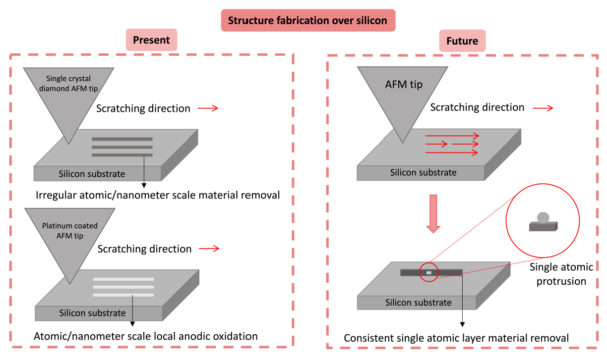
1. Introduction
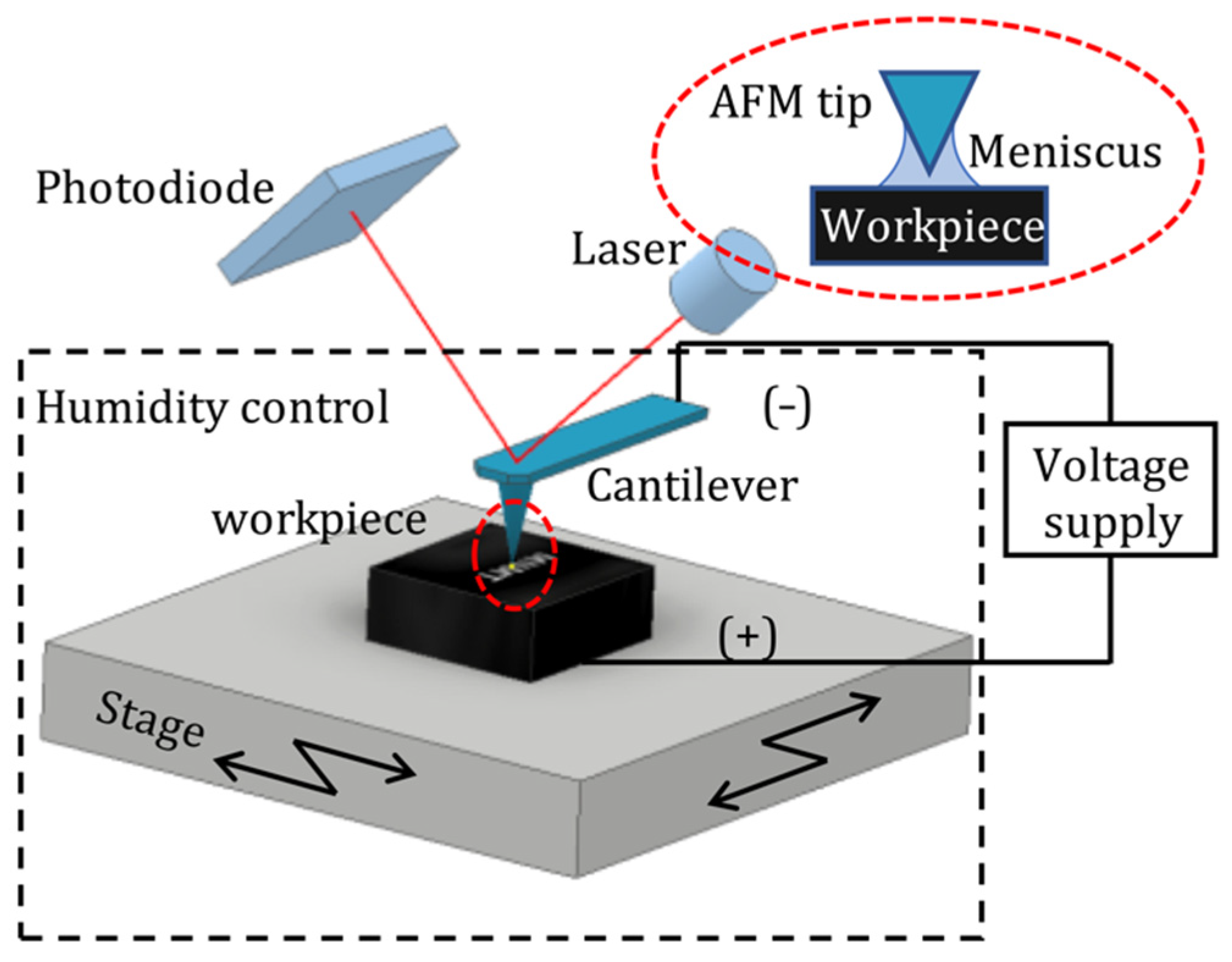
2. Materials and Methods
3. Results and Discussion
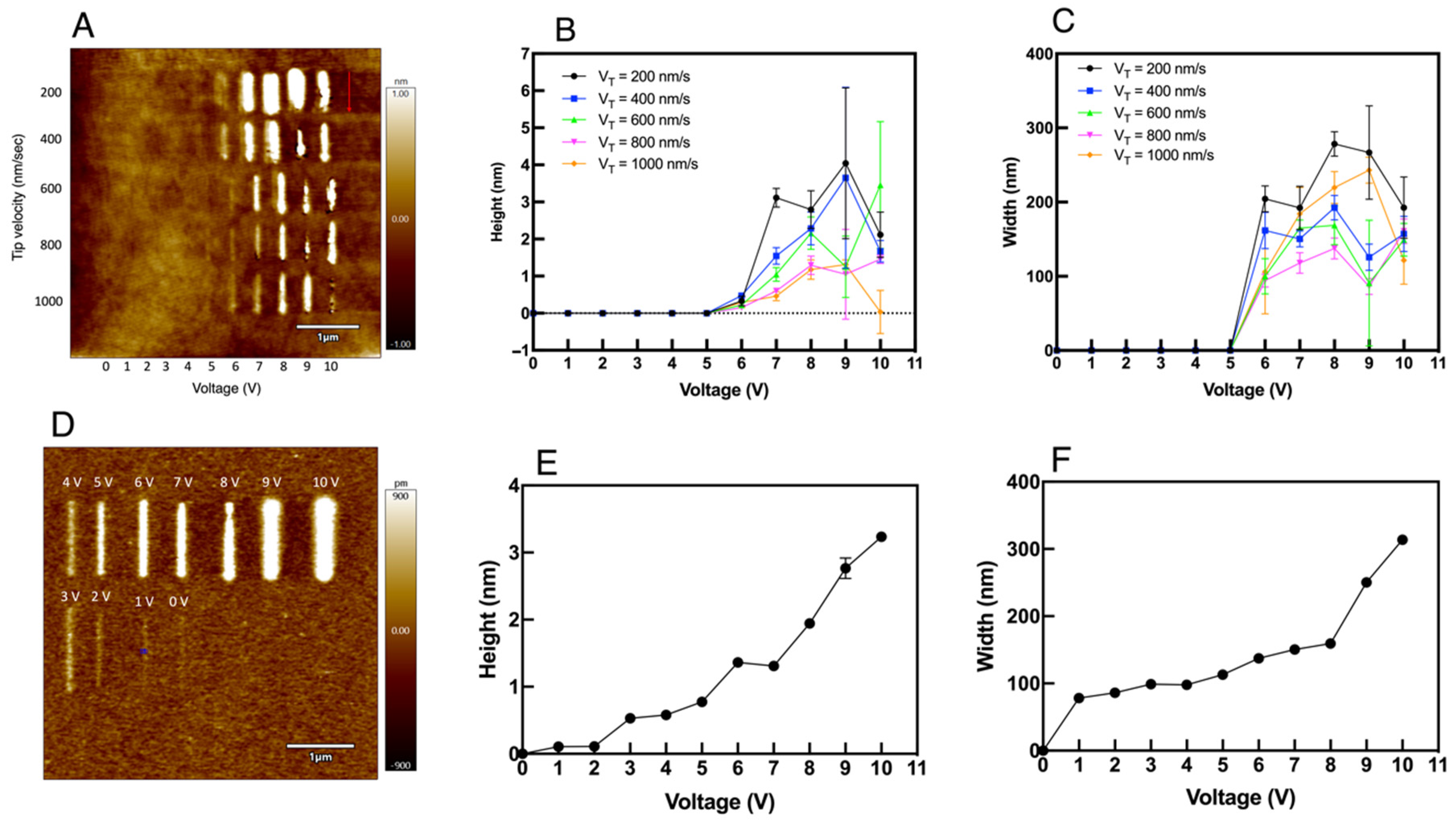
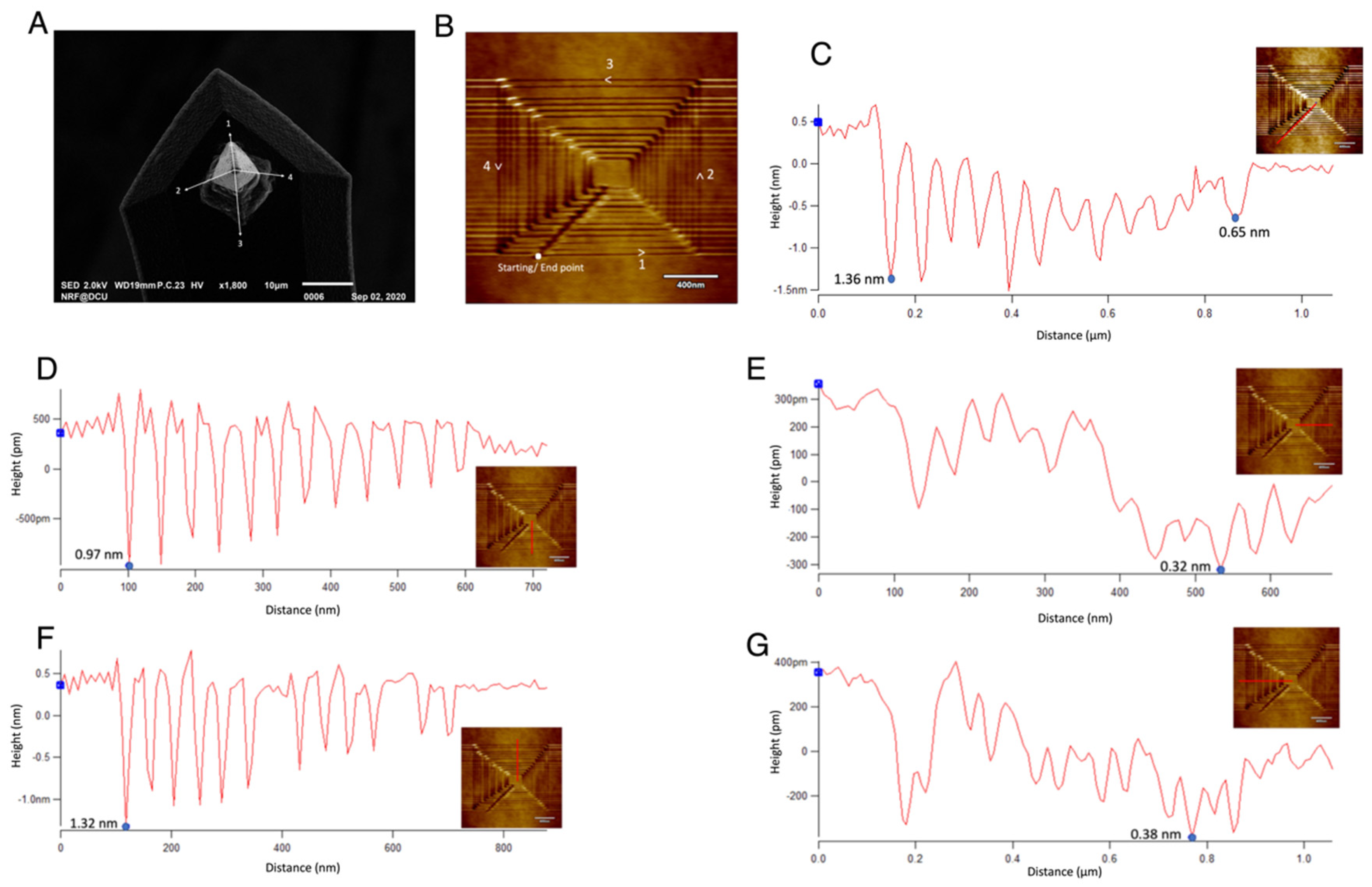
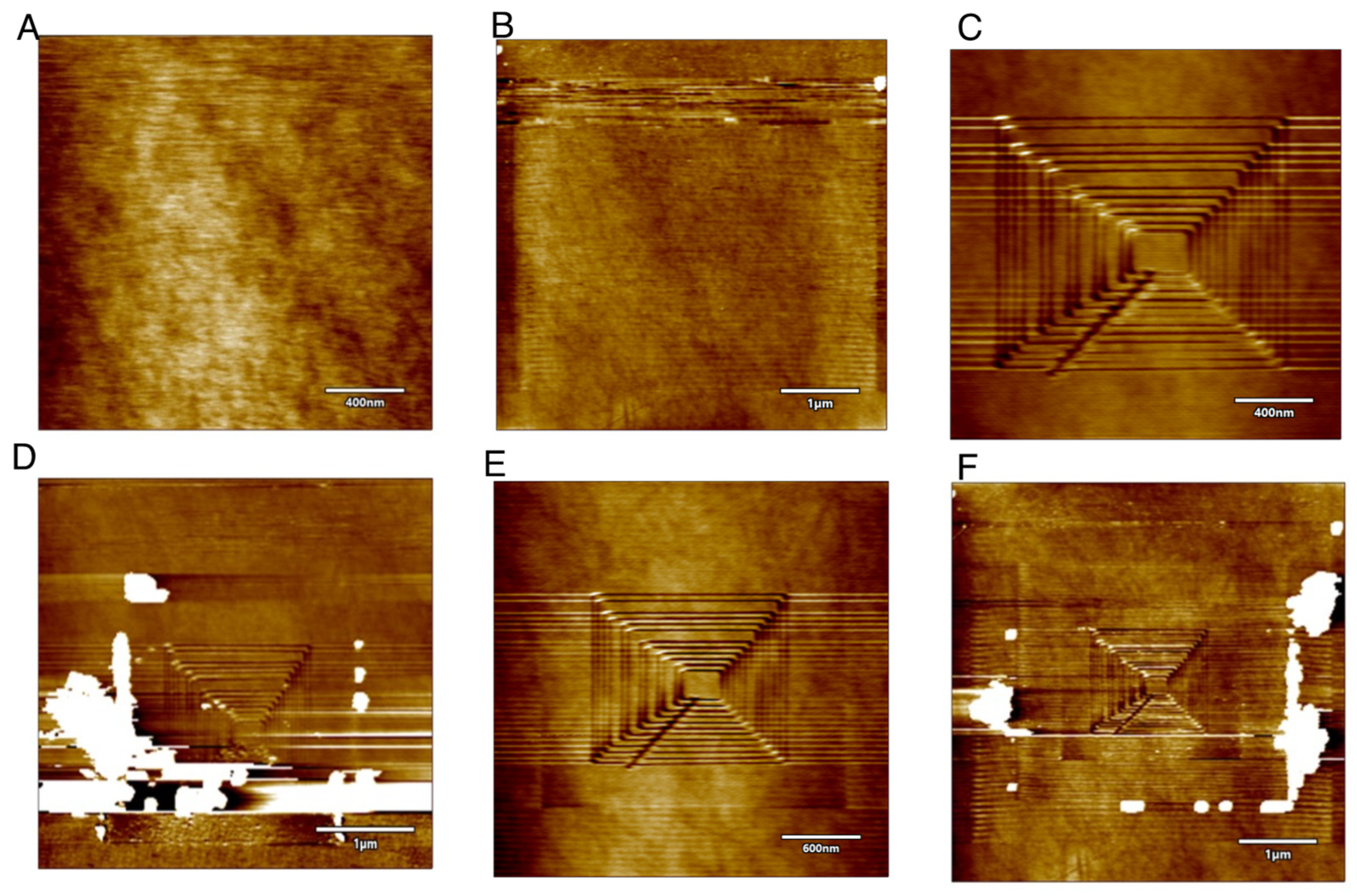
3.1. Scanning Probe Lithography (SPL) over Bare Silicon (with Native Oxide)
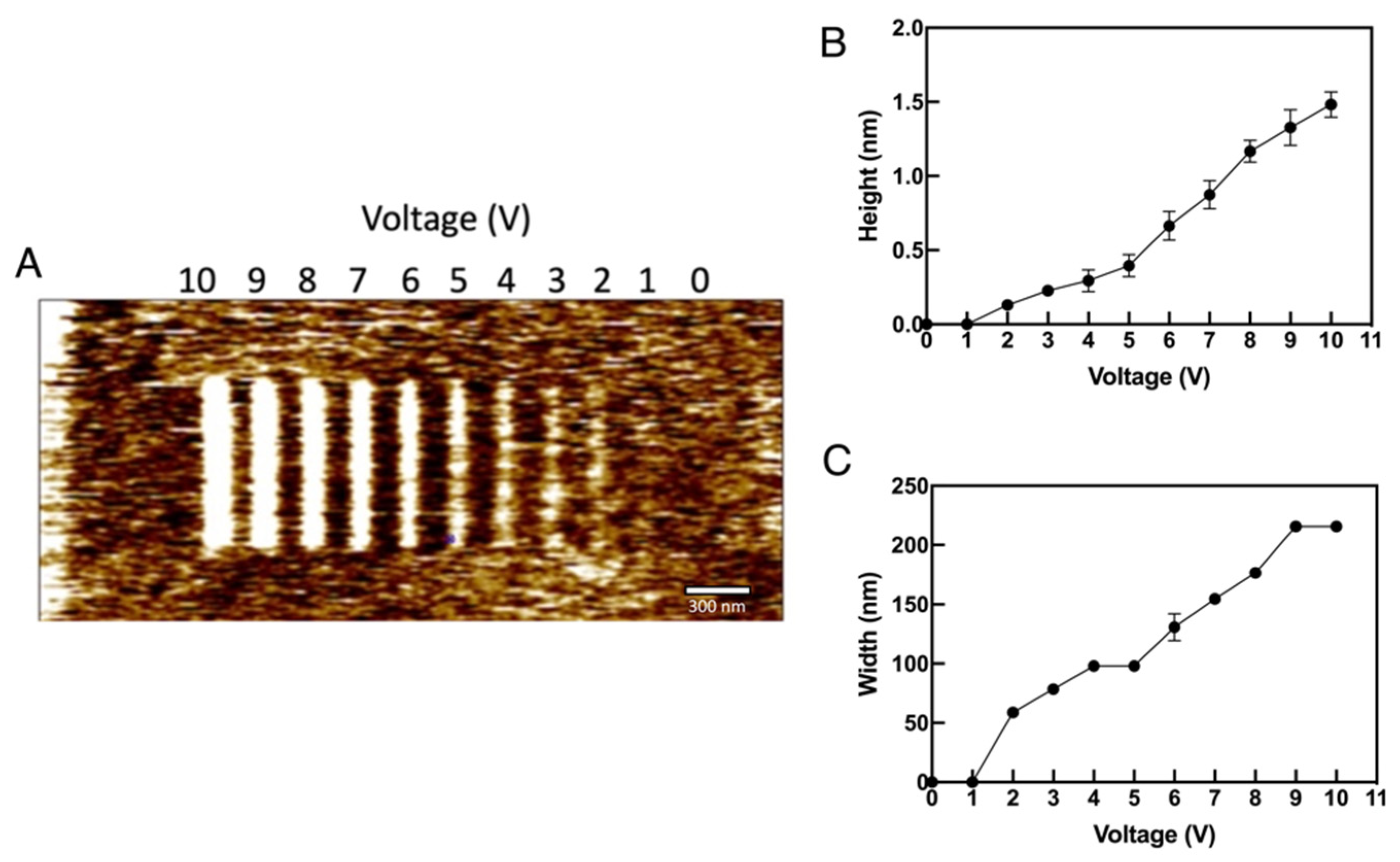
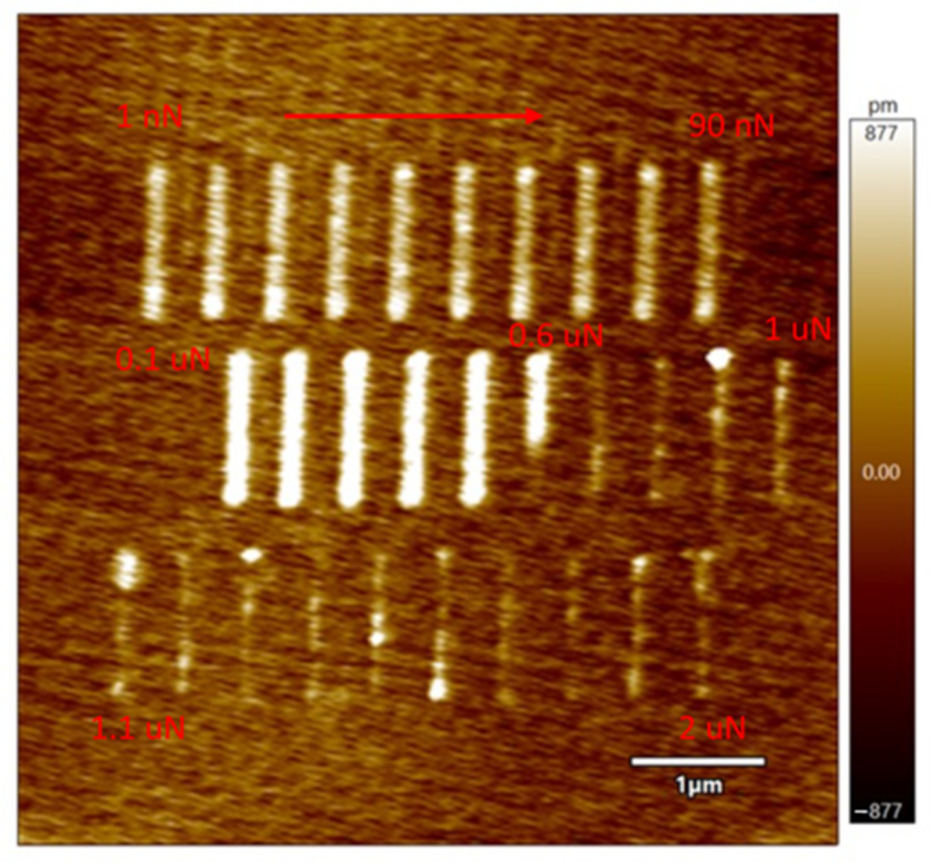
3.1.1. With Platinum Coated Tips
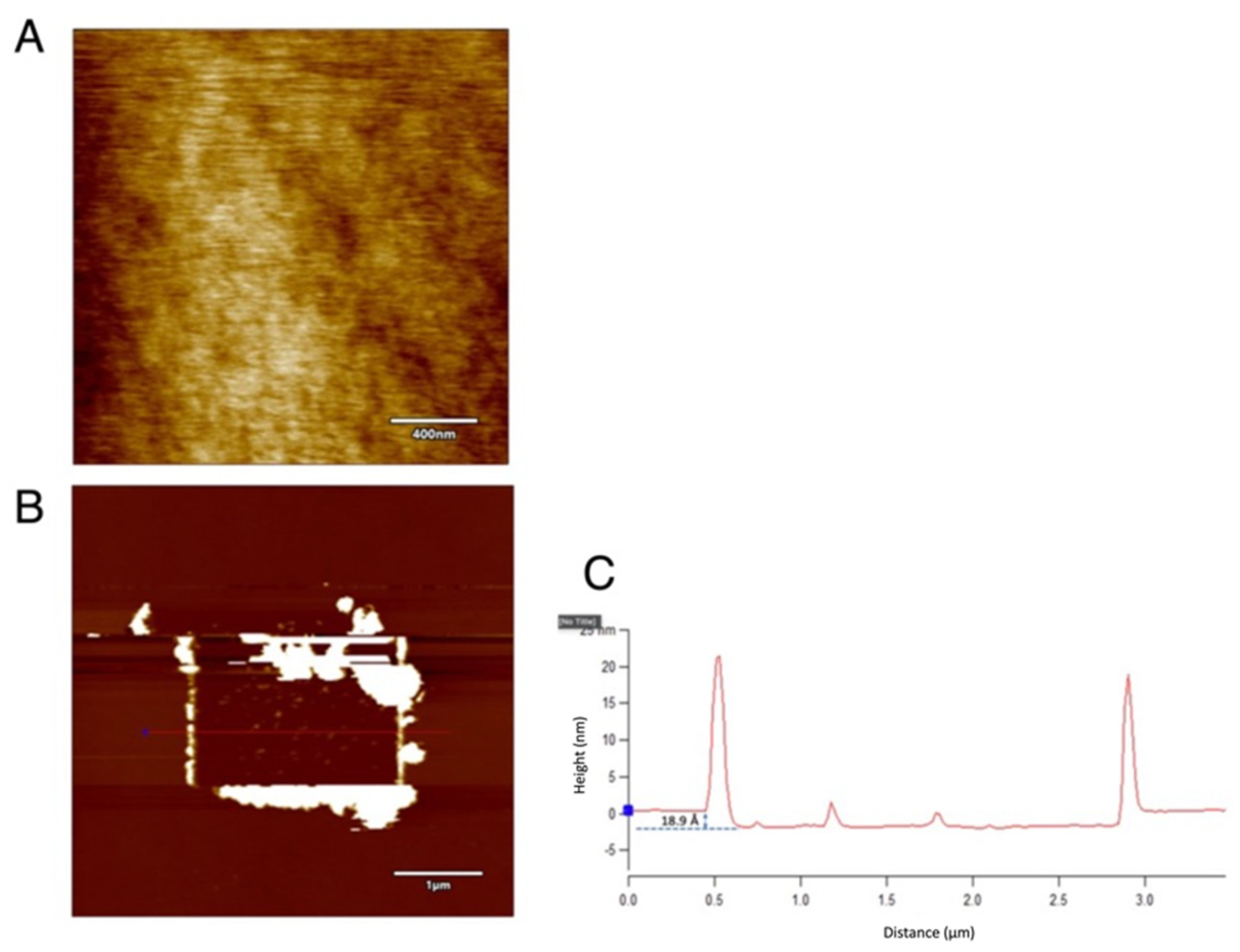
3.1.2. With Single Crystal Diamond Tip
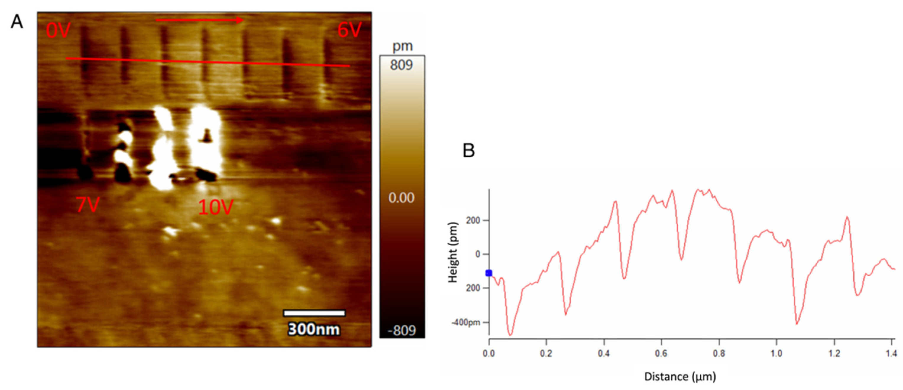
3.2. SPL over HF Treated Silicon
With Platinum and Single Crystal Diamond Tip
4. Conclusions
Author Contributions
Funding
Conflicts of Interest
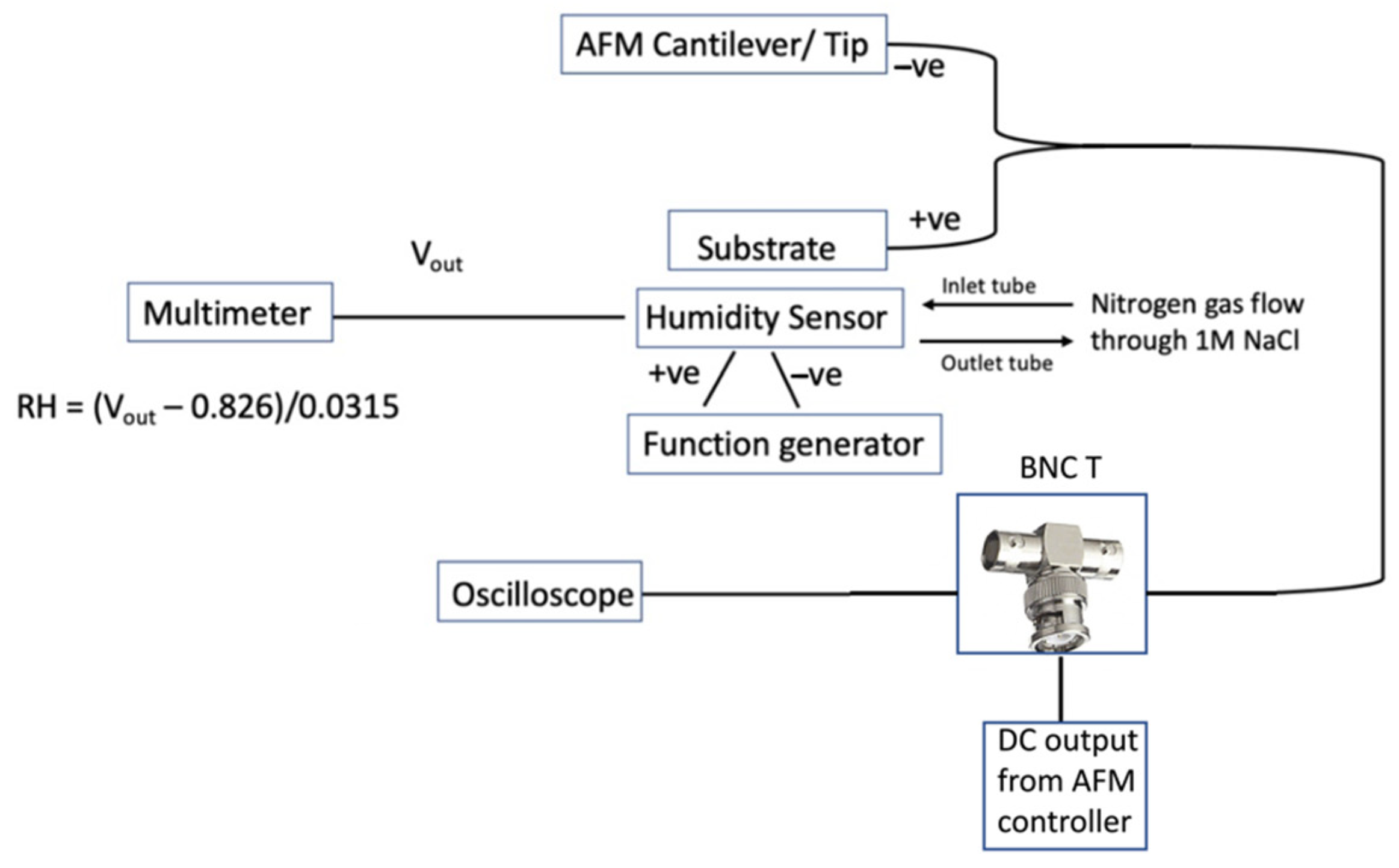
Appendix A. External Circuitry for Humidity Set-Up
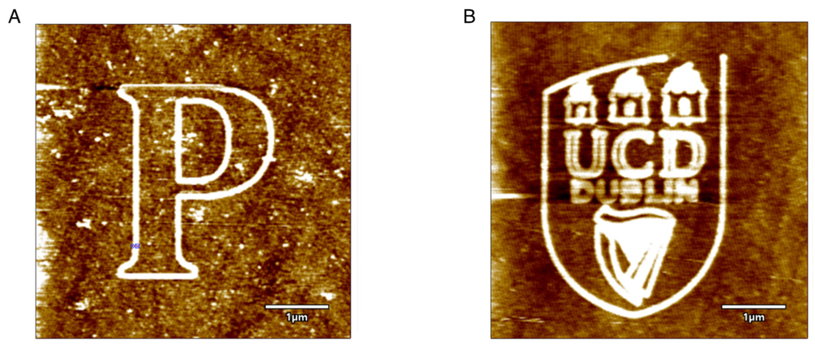
Appendix B. The Scratching of Concentric Square

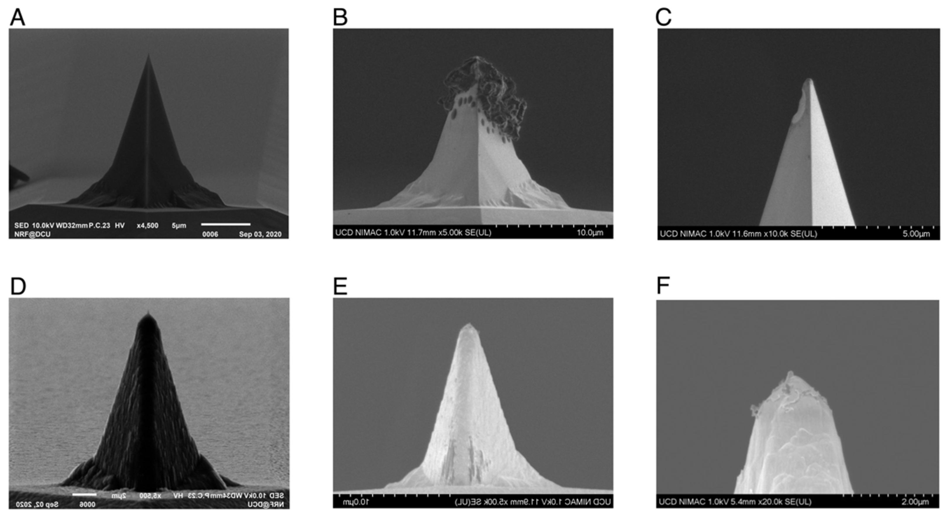
Appendix C. The Effects of Scratching on AFM Tips

References
- Avouris, P.; Hertel, T.; Martel, R. Atomic Force Microscope Tip-Induced Local Oxidation of Silicon: Kinetics, Mechanism, and Nanofabrication. Appl. Phys. Lett. 1997, 71, 285–287. [Google Scholar] [CrossRef]
- Bo, X.-Z.; Rokhinson, L.P.; Yin, H.; Tsui, D.C.; Sturm, J.C. Nanopatterning of Si/SiGe Electrical Devices by Atomic Force Microscopy Oxidation. Appl. Phys. Lett. 2002, 81, 3263–3265. [Google Scholar] [CrossRef] [Green Version]
- Avouris, P.; Martel, R.; Hertel, T.; Sandstrom, R. AFM-Tip-Induced and Current-Induced Local Oxidation of Silicon and Metals. Appl. Phys. A Mater. Sci. Process. 1998, 66, S659–S667. [Google Scholar] [CrossRef]
- Losilla, N.S.; Martínez, J.; García, R. Large Area Nanoscale Patterning of Silicon Surfaces by Parallel Local Oxidation. Nanotechnology 2009, 20, 475304. [Google Scholar] [CrossRef]
- Miyake, S.; Kim, J. Fabrication of Silicon Utilizing Mechanochemical Local Oxidation by Diamond Tip Sliding. Jpn. J. Appl. Phys. 2001, 40, L1247–L1249. [Google Scholar] [CrossRef]
- Tello, M.; García, R. Nano-Oxidation of Silicon Surfaces: Comparison of Noncontact and Contact Atomic-Force Microscopy Methods. Appl. Phys. Lett. 2001, 79, 424–426. [Google Scholar] [CrossRef] [Green Version]
- Notargiacomo, A.; Tseng, A.A. Assembling Uniform Oxide Lines and Layers by Overlapping Dots and Lines Using AFM Local Oxidation. In Proceedings of the 2009 9th IEEE Conference on Nanotechnology (IEEE-NANO), Genoa, Italy, 26–30 July 2009; pp. 907–910. [Google Scholar]
- Mathew, P.T.; Rodriguez, B.J.; Fang, F.Z. Atomic and Close-to-Atomic Scale Manufacturing: A Review on Atomic Layer Removal Methods Using Atomic Force Microscopy. Nanomanuf. Metrol. 2020, 3, 167–186. [Google Scholar] [CrossRef]
- Yamamoto, K.; Sato, K.; Sasano, J.; Nagai, M.; Shibata, T. Localized Etching of Silicon in Water Using a Catalytically Active Platinum-Coated Atomic Force Microscopy Probe. Precis. Eng. 2017, 50, 344–353. [Google Scholar] [CrossRef]
- Zheng, H.; Liu, Y.; Cao, F.; Wu, S.; Jia, S.; Cao, A.; Zhao, D.; Wang, J. Electron Beam-Assisted Healing of Nanopores in Magnesium Alloys. Sci. Rep. 2013, 3, 1920. [Google Scholar] [CrossRef] [PubMed]
- Aramesh, M. Ion-Beam Sculpting of Nanowires. Phys. Status Solidi RRL 2018, 12, 1700333. [Google Scholar] [CrossRef] [Green Version]
- Chen, W.; Zheng, L.; Teng, X.; Yang, K.; Huo, D. Cutting Mechanism Investigation in Vibration-Assisted Machining. Nanomanuf. Metrol. 2018, 1, 268–276. [Google Scholar] [CrossRef]
- Heidari, M.; Akbari, J.; Yan, J. Effects of Tool Rake Angle and Tool Nose Radius on Surface Quality of Ultraprecision Diamond-Turned Porous Silicon. J. Manuf. Process. 2019, 37, 321–331. [Google Scholar] [CrossRef]
- Dahlman, P.; Gunnberg, F.; Jacobson, M. The Influence of Rake Angle, Cutting Feed and Cutting Depth on Residual Stresses in Hard Turning. J. Mater. Process. Technol. 2004, 147, 181–184. [Google Scholar] [CrossRef]
- Rahman, M.A.; Amrun, M.R.; Rahman, M.; Kumar, A.S. Variation of Surface Generation Mechanisms in Ultra-Precision Machining Due to Relative Tool Sharpness (RTS) and Material Properties. Int. J. Mach. Tools Manuf. 2017, 115, 15–28. [Google Scholar] [CrossRef]
- Wang, M.; Duan, F. Atomic-Level Material Removal Mechanisms of Si(110) Chemical Mechanical Polishing: Insights from ReaxFF Reactive Molecular Dynamics Simulations. Langmuir 2021, 37, 2161–2169. [Google Scholar] [CrossRef]
- Liu, C.; He, W.; Chu, J.; Zhang, J.; Chen, X.; Xiao, J.; Xu, J. Molecular Dynamics Simulation on Cutting Mechanism in the Hybrid Machining Process of Single-Crystal Silicon. Nanoscale Res. Lett. 2021, 16, 66. [Google Scholar] [CrossRef]
- Yue, X.; Yang, X. Molecular Dynamics Simulation of the Material Removal Process and Gap Phenomenon of Nano EDM in Deionized Water. RSC Adv. 2015, 5, 66502–66510. [Google Scholar] [CrossRef]
- Fang, F.Z. Atomic and Close-to-Atomic Scale Manufacturing: Perspectives and Measures. Int. J. Extreme Manuf. 2020, 2, 030201. [Google Scholar] [CrossRef]
- Xie, W.; Fang, F.Z. On the Mechanism of Dislocation-Dominated Chip Formation in Cutting-Based Single Atomic Layer Removal of Monocrystalline Copper. Int. J. Adv. Manuf. Technol. 2020, 108, 1587–1599. [Google Scholar] [CrossRef]
- Xie, W.; Fang, F.Z. Mechanism of Atomic and Close-to-Atomic Scale Cutting of Monocrystalline Copper. Appl. Surf. Sci. 2020, 503, 144239. [Google Scholar] [CrossRef]
- Xie, W.; Fang, F.Z. Effect of Tool Edge Radius on Material Removal Mechanism in Atomic and Close-to-Atomic Scale Cutting. Appl. Surf. Sci. 2020, 504, 144451. [Google Scholar] [CrossRef]
- Xie, W.; Fang, F.Z. Cutting-Based Single Atomic Layer Removal Mechanism of Monocrystalline Copper: Atomic Sizing Effect. Nanomanuf. Metrol. 2019, 2, 241–252. [Google Scholar] [CrossRef]
- Xie, W.; Fang, F.Z. Cutting-Based Single Atomic Layer Removal Mechanism of Monocrystalline Copper: Edge Radius Effect. Nanoscale Res. Lett. 2019, 14, 370. [Google Scholar] [CrossRef]
- Chen, L.; Wen, J.; Zhang, P.; Yu, B.; Chen, C.; Ma, T.; Lu, X.; Kim, S.H.; Qian, L. Nanomanufacturing of Silicon Surface with a Single Atomic Layer Precision via Mechanochemical Reactions. Nat. Commun. 2018, 9, 1542. [Google Scholar] [CrossRef] [Green Version]
- Han, W.; Mathew, P.T.; Kolagatla, S.; Rodriguez, B.J.; Fang, F.Z. Toward Single-Atomic-Layer Lithography on Highly Oriented Pyrolytic Graphite Surfaces Using AFM-Based Electrochemical Etching. Nanomanuf. Metrol. 2022, 4. [Google Scholar] [CrossRef]
- Matei, G.A.; Thoreson, E.J.; Pratt, J.R.; Newell, D.B.; Burnham, N.A. Precision and Accuracy of Thermal Calibration of Atomic Force Microscopy Cantilevers. Rev. Sci. Instrum. 2006, 77, 083703. [Google Scholar] [CrossRef]
- Zhang, F.; Edwards, D.; Deng, X.; Wang, Y.; Kilpatrick, J.I.; Bassiri-Gharb, N.; Kumar, A.; Chen, D.; Gao, X.; Rodriguez, B.J. Investigation of AFM-Based Machining of Ferroelectric Thin Films at the Nanoscale. J. Appl. Phys. 2020, 127, 034103. [Google Scholar] [CrossRef]
- Kim, U.S.; Morita, N.; Lee, D.W.; Jun, M.; Park, J.W. The Possibility of Multi-Layer Nanofabrication via Atomic Force Microscope-Based Pulse Electrochemical Nanopatterning. Nanotechnology 2017, 28, 195302. [Google Scholar] [CrossRef]
- Dehzangi, A.; Larki, F.; Hutagalung, S.D.; Goodarz Naseri, M.; Majlis, B.Y.; Navasery, M.; Hamid, N.A.; Noor, M.M. Impact of Parameter Variation in Fabrication of Nanostructure by Atomic Force Microscopy Nanolithography. PLoS ONE 2013, 8, e65409. [Google Scholar] [CrossRef] [PubMed]
- Cabrera, N.; Mott, N.F. Theory of the Oxidation of Metals. Rep. Prog. Phys. 1949, 12, 163–184. [Google Scholar] [CrossRef]
- Temiryazev, A. Pulse Force Nanolithography on Hard Surfaces Using Atomic Force Microscopy with a Sharp Single-Crystal Diamond Tip. Diam. Relat. Mater. 2014, 48, 60–64. [Google Scholar] [CrossRef] [Green Version]


Publisher’s Note: MDPI stays neutral with regard to jurisdictional claims in published maps and institutional affiliations. |
© 2022 by the authors. Licensee MDPI, Basel, Switzerland. This article is an open access article distributed under the terms and conditions of the Creative Commons Attribution (CC BY) license (https://creativecommons.org/licenses/by/4.0/).
Share and Cite
Mathew, P.T.; Han, W.; Rodriguez, B.J.; Fang, F. Structure Fabrication on Silicon at Atomic and Close-To-Atomic Scale Using Atomic Force Microscopy: Implications for Nanopatterning and Nanodevice Fabrication. Micromachines 2022, 13, 524. https://doi.org/10.3390/mi13040524
Mathew PT, Han W, Rodriguez BJ, Fang F. Structure Fabrication on Silicon at Atomic and Close-To-Atomic Scale Using Atomic Force Microscopy: Implications for Nanopatterning and Nanodevice Fabrication. Micromachines. 2022; 13(4):524. https://doi.org/10.3390/mi13040524
Chicago/Turabian StyleMathew, Paven Thomas, Wei Han, Brian J. Rodriguez, and Fengzhou Fang. 2022. "Structure Fabrication on Silicon at Atomic and Close-To-Atomic Scale Using Atomic Force Microscopy: Implications for Nanopatterning and Nanodevice Fabrication" Micromachines 13, no. 4: 524. https://doi.org/10.3390/mi13040524
APA StyleMathew, P. T., Han, W., Rodriguez, B. J., & Fang, F. (2022). Structure Fabrication on Silicon at Atomic and Close-To-Atomic Scale Using Atomic Force Microscopy: Implications for Nanopatterning and Nanodevice Fabrication. Micromachines, 13(4), 524. https://doi.org/10.3390/mi13040524