

Rapid Fabrication of Low-Cost Thermal Bubble-Driven Micro-Pumps
 , , , , and
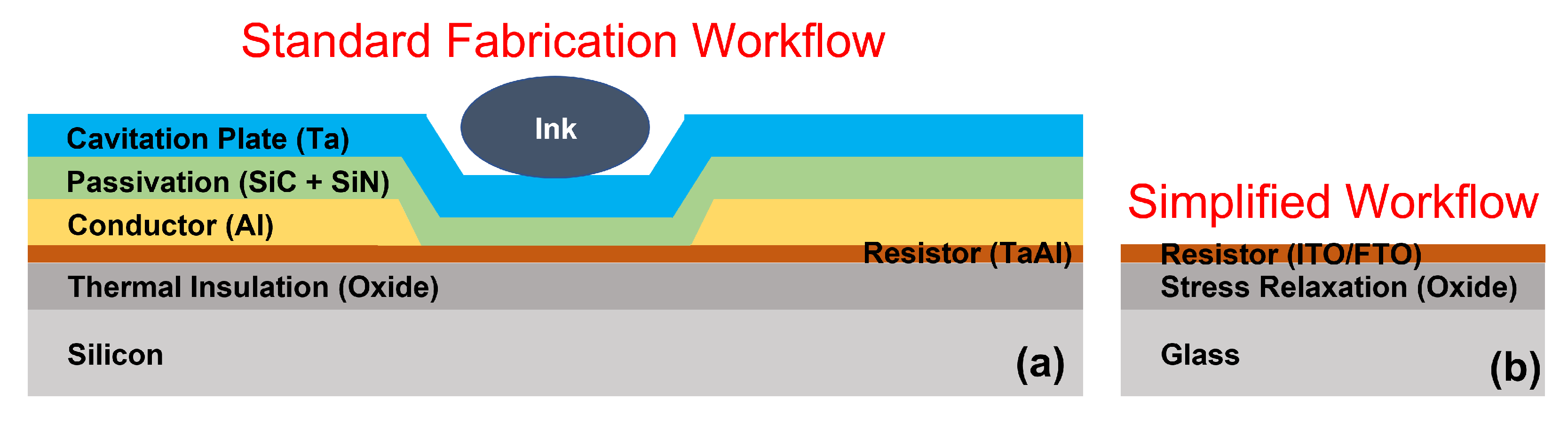
Abstract
1. Introduction
2. Materials and Methods
2.1. Resistor Fabrication
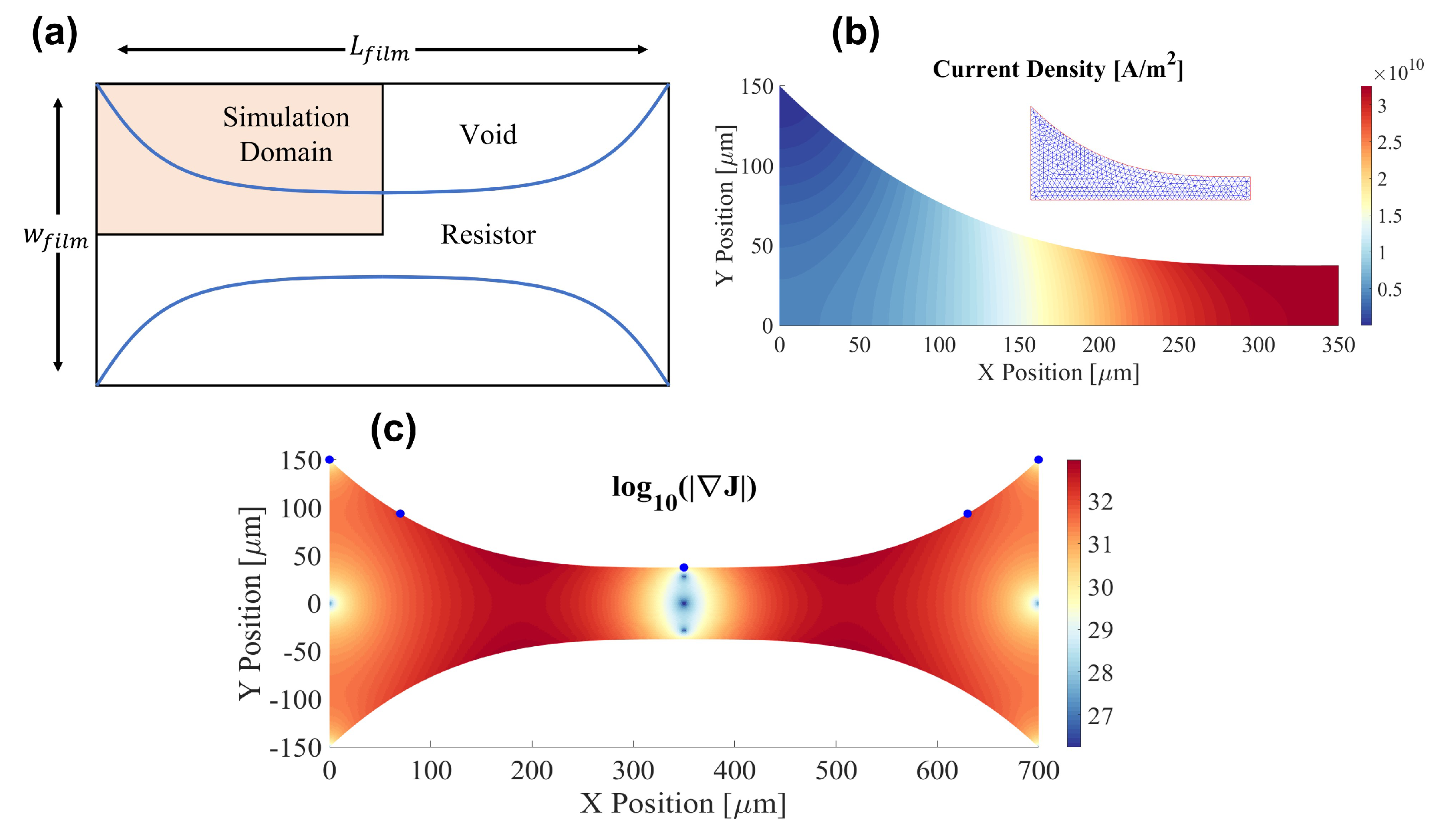
2.1.1. Single Material Resistor Design Optimization
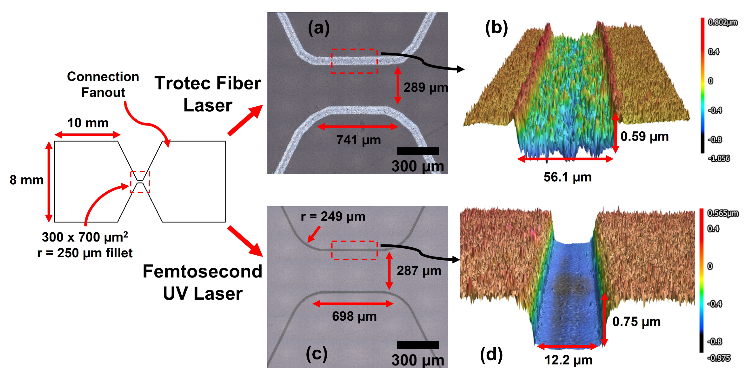
2.1.2. Laser Cutting of Resistors
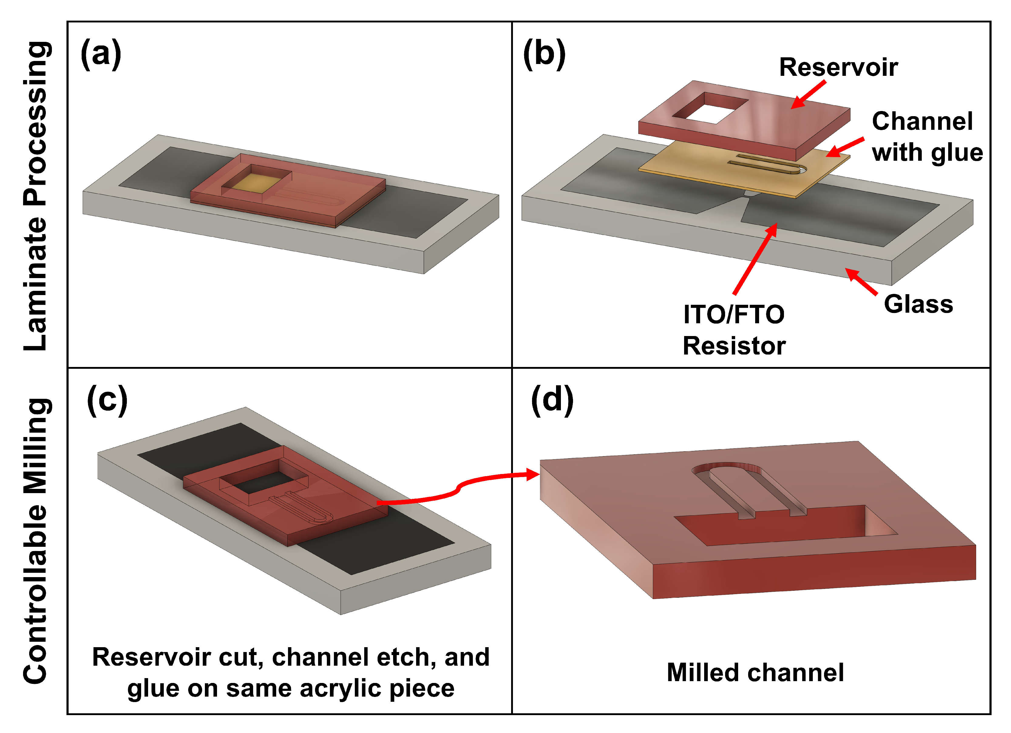
2.2. Microfluidic Fabrication
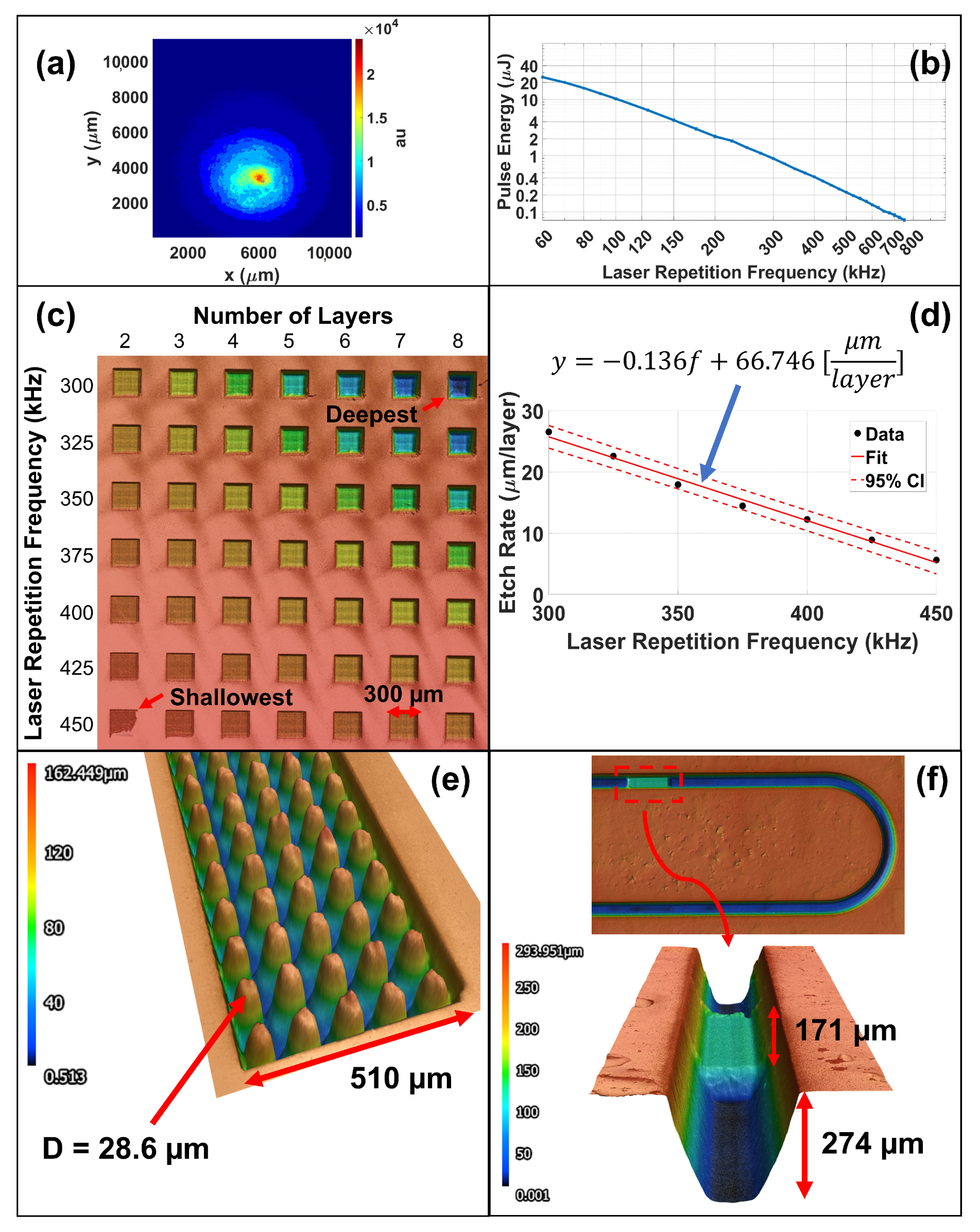
2.3. Femtosecond UV Laser Beam Profile and Material Etch Rates
2.4. Electrical Setup
2.5. Imaging Setup
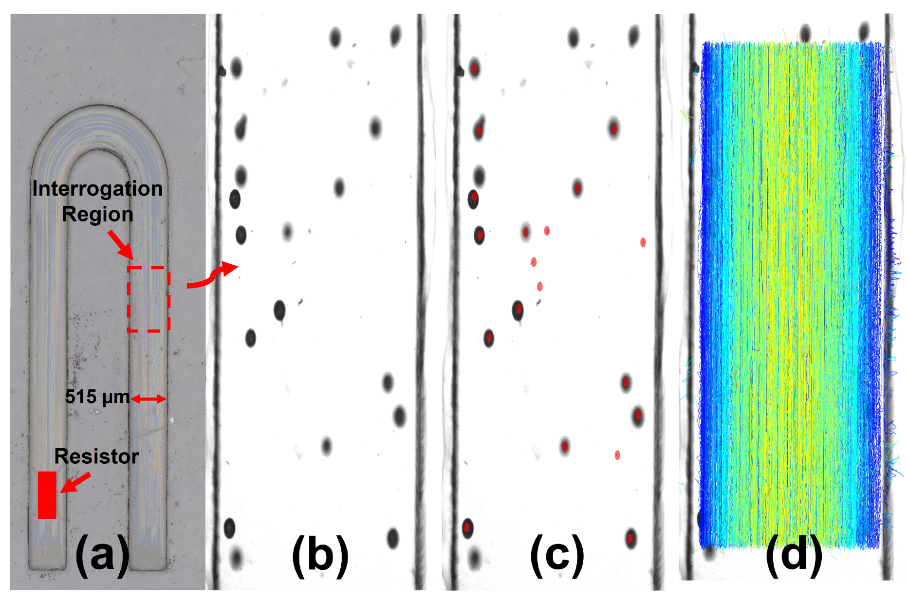
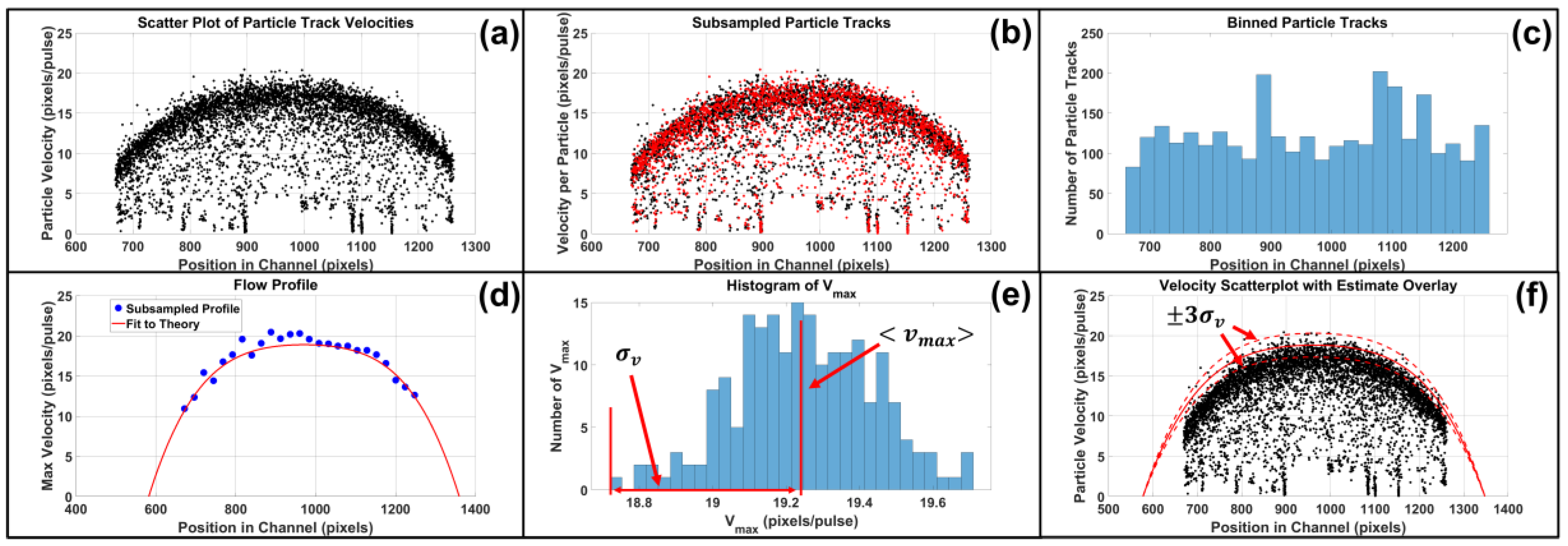
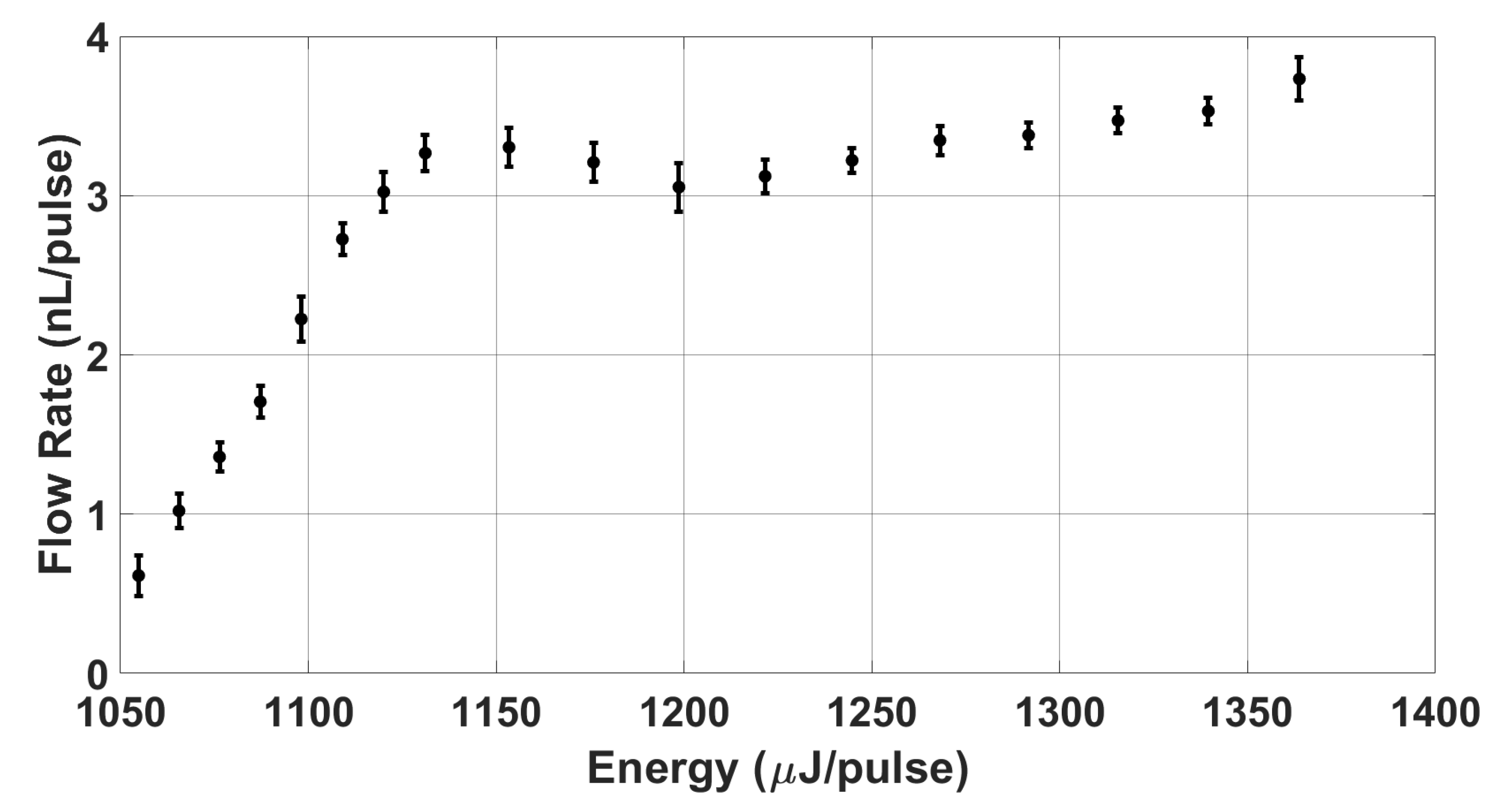
2.6. Particle Tracking and Flow Rate Characterization
3. Results
3.1. Electrical Signal Integrity
- A solid back copper ground plane is used to ensure that the ground is at a common voltage even with large currents flowing.
- Digital return currents from the Analog Discovery and gate drivers are separated from interfering with the analog return currents from the power MOSFETs. This is done by separate placement of components and traces on the PCB.
- A 27 series gate resistor is used to “slow down” the power MOSFET turn on/off time to reduce gate ringing.
- Gate drivers with internal Miller Clamps are used to reduce capacitive ringing on turn off.
- Flyback Schottky diodes are used to minimize inductive ringing caused by connecting wires from the main power supply to the thin film resistors.
- Large bypass capacitors (100 F and 10 F) are used to maintain a steady supply voltage and provide large, transient current draws thus reducing transient spikes from the power supply.
- Smaller bypass capacitors (0.1 F and 10 F) are used to stabilize the supply voltage to the gate driver and mitigate high frequency voltage spikes in the power supplies.
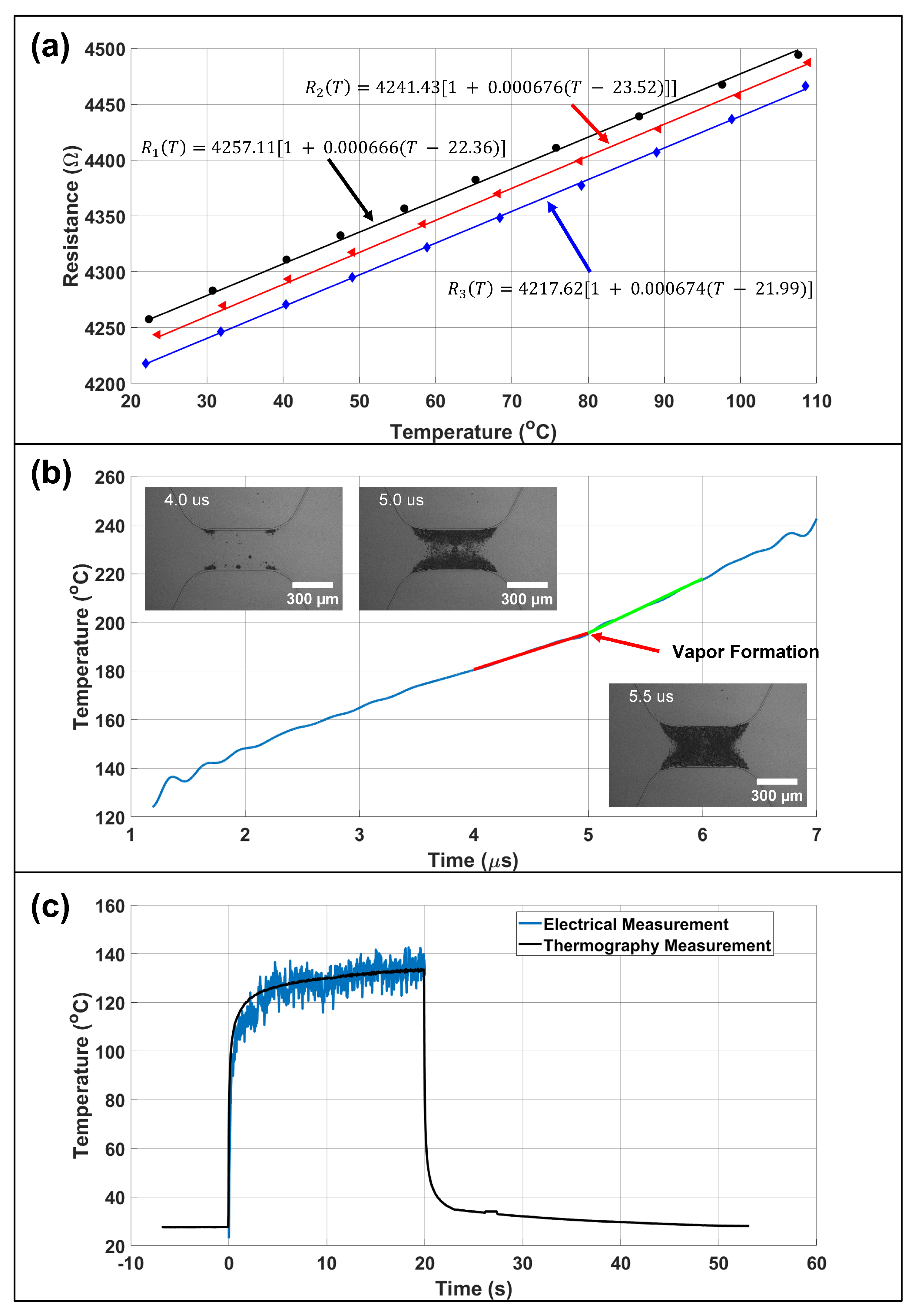
3.2. Temperature Sensing
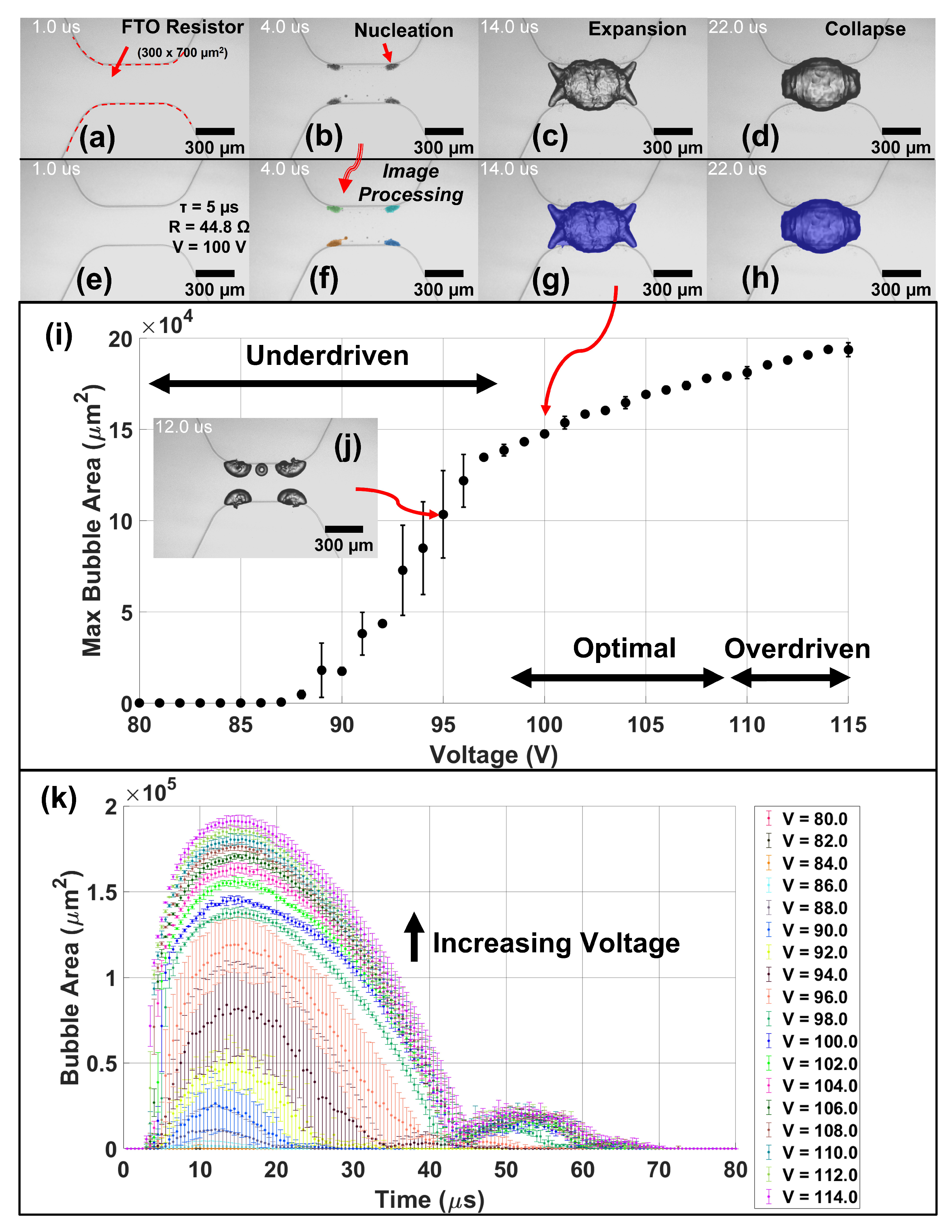
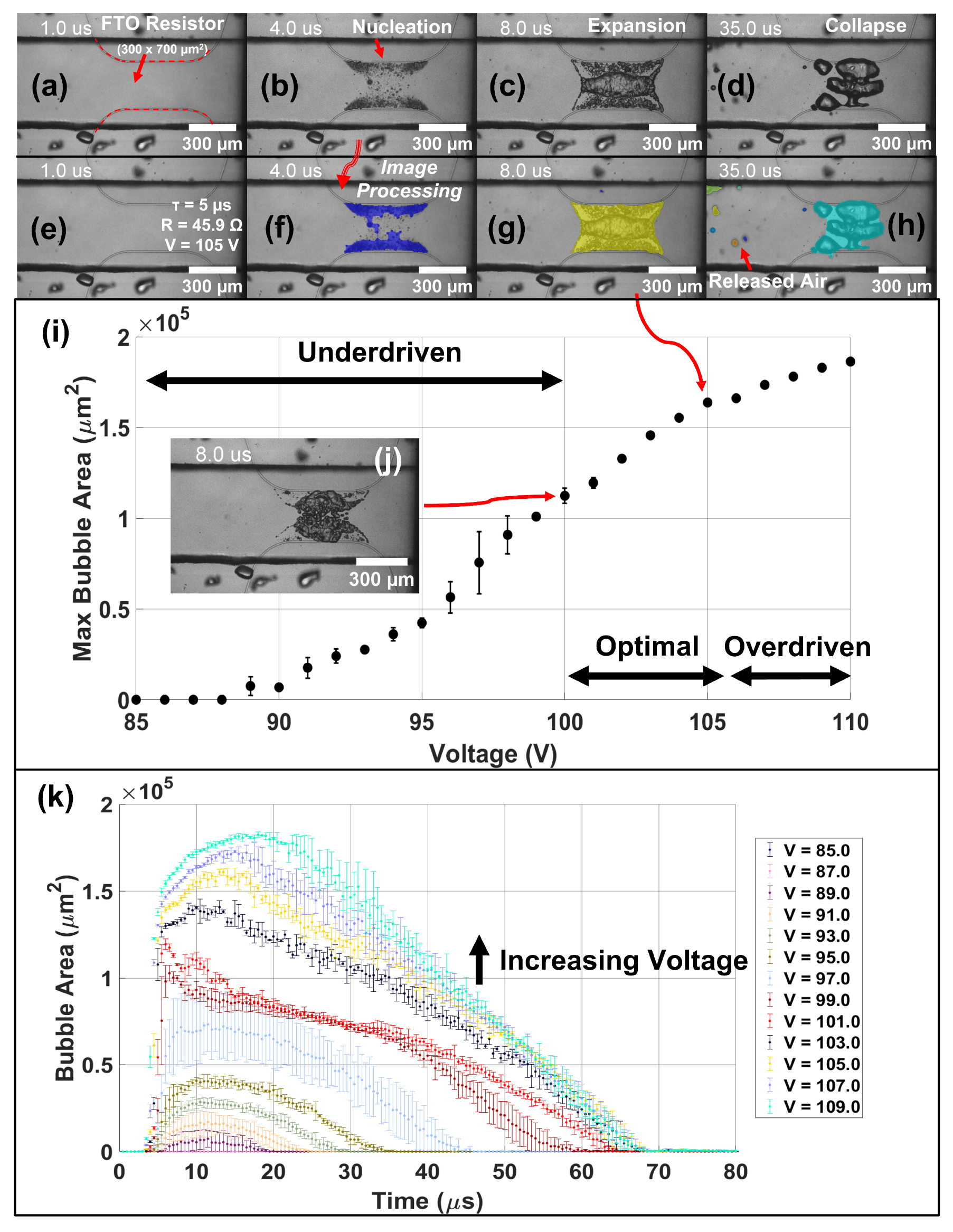
3.3. Open Reservoir vs. Confined Bubble Dynamics
3.4. Thermal Bubble-Driven Micro-Pumps
4. Conclusions
Supplementary Materials
Author Contributions
Funding
Data Availability Statement
Acknowledgments
Conflicts of Interest
References
- Yuan, H.; Prosperetti, A. The pumping effect of growing and collapsing bubbles in a tube. J. Micromech. Microeng. 1999, 9, 402–413. [Google Scholar] [CrossRef]
- Govyadinov, A.; Kornilovitch, P.; Markel, D.; Torniainen, E. Single-pulse dynamics and flow rates of inertial micropumps. Microfluid. Nanofluid. 2016, 20, 73. [Google Scholar] [CrossRef]
- Kornilovitch, P.; Govyadinov, A.; Markel, D.; Torniainen, E. One-dimensional model of inertial pumping. Phys. Rev. E 2013, 87, 023012. [Google Scholar] [CrossRef] [PubMed]
- Hayes, B.; Govyadinov, A.; Kornilovitch, P. Microfluidic switchboards with integrated inertial pumps. Microfluid. Nanofluid. 2018, 22, 15. [Google Scholar] [CrossRef]
- Torniainen, E.; Govyadinov, A.; Markel, D.; Kornilovitch, P. Bubble-driven inertial micropump. Phys. Fluids 2012, 24, 122003. [Google Scholar] [CrossRef]
- Mohammed, M.I.; Haswell, S.; Gibson, I. Lab-on-a-chip or Chip-in-a-lab: Challenges of Commercialization Lost in Translation. Procedia Technol. 2015, 20, 54–59. [Google Scholar] [CrossRef]
- Unger, M.A.; Chou, H.P.; Thorsen, T.; Scherer, A.; Quake, S.R. Monolithic Microfabricated Valves and Pumps by Multilayer Soft Lithography. Science 2000, 288, 113–116. [Google Scholar] [CrossRef]
- Puigmartí-Luis, J.; Rubio-Martínez, M.; Imaz, I.; Cvetković, B.Z.; Abad, L.; Pérez del Pino, A.; Maspoch, D.; Amabilino, D.B. Localized, Stepwise Template Growth of Functional Nanowires from an Amino Acid-Supported Framework in a Microfluidic Chip. ACS Nano 2014, 8, 818–826. [Google Scholar] [CrossRef]
- Hsieh, L.Y.; Hsieh, T.J. A Throughput Management System for Semiconductor Wafer Fabrication Facilities: Design, Systems and Implementation. Processes 2018, 6, 16. [Google Scholar] [CrossRef]
- May, M.C.; Maucher, S.; Holzer, A.; Kuhnle, A.; Lanza, G. Data analytics for time constraint adherence prediction in a semiconductor manufacturing use-case. Procedia CIRP 2021, 100, 49–54. [Google Scholar] [CrossRef]
- Convery, N.; Gadegaard, N. 30 years of microfluidics. Micro Nano Eng. 2019, 2, 76–91. [Google Scholar] [CrossRef]
- Waheed, S.; Cabot, J.M.; Macdonald, N.P.; Lewis, T.; Guijt, R.M.; Paull, B.; Breadmore, M.C. 3D printed microfluidic devices: Enablers and barriers. Lab Chip 2016, 16, 1993–2013. [Google Scholar] [CrossRef] [PubMed]
- Ory, E.; Yuan, H.; Prosperetti, A.; Popinet, S.; Zaleski, S. Growth and collapse of a vapor bubble in a narrow tube. Phys. Fluids 2000, 12, 1268–1277. [Google Scholar] [CrossRef]
- Yin, Z.; Prosperetti, A. ‘Blinking bubble’ micropump with microfabricated heaters. J. Micromech. Microeng. 2005, 15, 1683. [Google Scholar] [CrossRef]
- Einat, M.; Grajower, M. Microboiling Measurements of Thermal-Inkjet Heaters. J. Microelectromech. Syst. 2010, 19, 391–395. [Google Scholar] [CrossRef]
- Hayes, B.; Whiting, G.L.; MacCurdy, R. Modeling of contactless bubble–bubble interactions in microchannels with integrated inertial pumps. Phys. Fluids 2021, 33, 042002. [Google Scholar] [CrossRef]
- Liu, B.; Sun, J.; Li, D.; Zhe, J.; Oh, K.W. A high flow rate thermal bubble-driven micropump with induction heating. Microfluid. Nanofluid. 2016, 20, 155. [Google Scholar] [CrossRef]
- Liu, B.; Ma, C.; Yang, J.; Li, D.; Liu, H. Study on the Heat Source Insulation of a Thermal Bubble-Driven Micropump with Induction Heating. Micromachines 2021, 12, 1040. [Google Scholar] [CrossRef]
- Hayes, B.; Hayes, A.; Rolleston, M.; Ferreira, A.; Kirsher, J. Pulsatory mixing of laminar flow using bubble-driven micro-pumps. In Proceedings of the ASME International Mechanical Engineering Congress and Exposition, Pittsburgh, PA, USA, 9–15 November 2018. [Google Scholar]
- Sourtiji, E.; Peles, Y. A micro-synthetic jet in a microchannel using bubble growth and collapse. Appl. Therm. Eng. 2019, 160, 114084. [Google Scholar] [CrossRef]
- Aden, J.; Bohórquez, J.A.; Collins, D.; Crook, M.; Garcia, A.; Hess, U.E. The Third-generation Hp Thermal Inkjet Printhead. Hewlett-Packard J. 1994, 45, 41–45. [Google Scholar]
- Hoefemann, H.; Wadle, S.; Bakhtina, N.; Kondrashov, V.; Wangler, N.; Zengerle, R. Sorting and lysis of single cells by BubbleJet technology. Sens. Actuator B Chem. 2012, 168, 442–445. [Google Scholar] [CrossRef]
- Pritchard, R.H.; Zhukov, A.A.; Fullerton, J.N.; Want, A.J.; Hussain, F.; la Cour, M.F.; Bashtanov, M.E.; Gold, R.D.; Hailes, A.; Banham-Hall, E.; et al. Cell sorting actuated by a microfluidic inertial vortex. Lab Chip 2019, 19, 2456–2465. [Google Scholar] [CrossRef] [PubMed]
- Solis, L.H.; Ayala, Y.; Portillo, S.; Varela-Ramirez, A.; Aguilera, R.; Boland, T. Thermal inkjet bioprinting triggers the activation of the VEGF pathway in human microvascular endothelial cells in vitro. Biofabrication 2019, 11, 045005. [Google Scholar] [CrossRef] [PubMed]
- Bar-Levav, E.; Witman, M.; Einat, M. Thin-Film MEMS Resistors with Enhanced Lifetime for Thermal Inkjet. Micromachines 2020, 11, 499. [Google Scholar] [CrossRef] [PubMed]
- Chung, C.K.; Chang, E.C.; Zou, B.H. Formation and observation of thermal bubble from multilayer heating material. In Proceedings of the 2010 IEEE 5th International Conference on Nano/Micro Engineered and Molecular Systems, Xiamen, China, 20–23 January 2010; pp. 684–687. [Google Scholar] [CrossRef]
- Lin, L.; Pisano, A.P.; Carey, V.P. Thermal Bubble Formation on Polysilicon Micro Resistors. J. Heat Transf. 1998, 120, 735–742. [Google Scholar] [CrossRef]
- Tsai, J.H.; Lin, L. A thermal-bubble-actuated micronozzle-diffuser pump. J. Microelectromech. Syst. 2002, 11, 665–671. [Google Scholar] [CrossRef]
- Lin, L.; Pisano, A.P. Thermal bubble powered microactuators. Microsyst. Technol. 1994, 1, 51–58. [Google Scholar] [CrossRef]
- van den Broek, D.; Elwenspoek, M. Explosive micro-bubble actuator. Sens. Actuators A Phys. 2008, 145–146, 387–393. [Google Scholar] [CrossRef][Green Version]
- Abrishamkar, A.; Paradinas, M.; Bailo, E.; Rodriguez-Trujillo, R.; Pfattner, R.; Rossi, R.M.; Ocal, C.; deMello, A.J.; Amabilino, D.B.; Puigmartí-Luis, J. Microfluidic pneumatic cages: A novel approach for in-chip crystal trapping, manipulation and controlled chemical treatment. JoVE J. Vis. Exp. 2016, 113, e54193. [Google Scholar] [CrossRef]
- Jafferis, N.T.; Jayaram, K.; York, P.A.; Wood, R.J. A streamlined fabrication process for high energy density piezoelectric bending actuators. Sens. Actuators A Phys. 2021, 332, 113155. [Google Scholar] [CrossRef]
- Jayaram, K.; Shum, J.; Castellanos, S.; Helbling, E.F.; Wood, R.J. Scaling down an insect-size microrobot, HAMR-VI into HAMR-Jr. In Proceedings of the 2020 IEEE International Conference on Robotics and Automation (ICRA), Paris, France, 31 May–31 August 2020; pp. 10305–10311. [Google Scholar]
- Baum, M.; Strauß, J.; Grüßel, F.; Alexeev, I.; Schmidt, M. Generation of phase-only holograms by laser ablation of nanoparticulate ITO layers. J. Opt. 2014, 16, 125706. [Google Scholar] [CrossRef]
- Hu, Z.; Zhang, J.; Hao, Z.; Hao, Q.; Geng, X.; Zhao, Y. Highly efficient organic photovoltaic devices using F-doped SnO2 anodes. Appl. Phys. Lett. 2011, 98, 123302. [Google Scholar] [CrossRef]
- Nath, P.; Fung, D.; Kunde, Y.A.; Zeytun, A.; Branch, B.; Goddard, G. Rapid prototyping of robust and versatile microfluidic components using adhesive transfer tapes. Lab Chip 2010, 10, 2286–2291. [Google Scholar] [CrossRef] [PubMed]
- Suriano, R.; Kuznetsov, A.; Eaton, S.M.; Kiyan, R.; Cerullo, G.; Osellame, R.; Chichkov, B.N.; Levi, M.; Turri, S. Femtosecond laser ablation of polymeric substrates for the fabrication of microfluidic channels. Appl. Surf. Sci. 2011, 257, 6243–6250. [Google Scholar] [CrossRef]
- Paschotta, R. Field Guide to Lasers/Rüdiger Paschotta; SPIE Press: Bellingham, WA, USA, 2008. [Google Scholar]
- Crocker, J.C.; Grier, D.G. Methods of Digital Video Microscopy for Colloidal Studies. J. Colloid Interface Sci. 1996, 179, 298–310. [Google Scholar] [CrossRef]
- Kornilovitch, P.E.; Cochell, T.; Govyadinov, A.N. Temperature dependence of inertial pumping in microchannels. Phys. Fluids 2022, 34, 022003. [Google Scholar] [CrossRef]
- van den Broek, D.M.; Elwenspoek, M. Bubble nucleation in an explosive micro-bubble actuator. J. Micromech. Microeng. 2008, 18, 064003. [Google Scholar] [CrossRef]


Publisher’s Note: MDPI stays neutral with regard to jurisdictional claims in published maps and institutional affiliations. |
© 2022 by the authors. Licensee MDPI, Basel, Switzerland. This article is an open access article distributed under the terms and conditions of the Creative Commons Attribution (CC BY) license (https://creativecommons.org/licenses/by/4.0/).
Share and Cite
Hayes, B.; Smith, L.; Kabutz, H.; Hayes, A.C.; Whiting, G.L.; Jayaram, K.; MacCurdy, R. Rapid Fabrication of Low-Cost Thermal Bubble-Driven Micro-Pumps. Micromachines 2022, 13, 1634. https://doi.org/10.3390/mi13101634
Hayes B, Smith L, Kabutz H, Hayes AC, Whiting GL, Jayaram K, MacCurdy R. Rapid Fabrication of Low-Cost Thermal Bubble-Driven Micro-Pumps. Micromachines. 2022; 13(10):1634. https://doi.org/10.3390/mi13101634
Chicago/Turabian StyleHayes, Brandon, Lawrence Smith, Heiko Kabutz, Austin C. Hayes, Gregory L. Whiting, Kaushik Jayaram, and Robert MacCurdy. 2022. "Rapid Fabrication of Low-Cost Thermal Bubble-Driven Micro-Pumps" Micromachines 13, no. 10: 1634. https://doi.org/10.3390/mi13101634
APA StyleHayes, B., Smith, L., Kabutz, H., Hayes, A. C., Whiting, G. L., Jayaram, K., & MacCurdy, R. (2022). Rapid Fabrication of Low-Cost Thermal Bubble-Driven Micro-Pumps. Micromachines, 13(10), 1634. https://doi.org/10.3390/mi13101634