High-Efficiency, Wide Working Bandwidth Antenna Based on SOI Platform for Optical Phased Array


Abstract
:1. Introduction
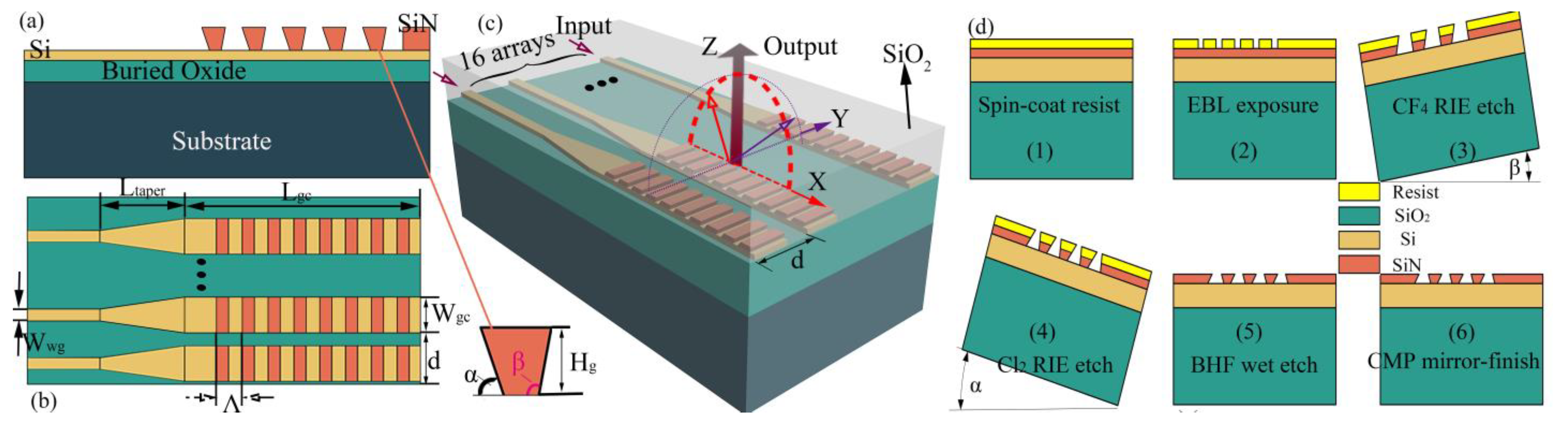
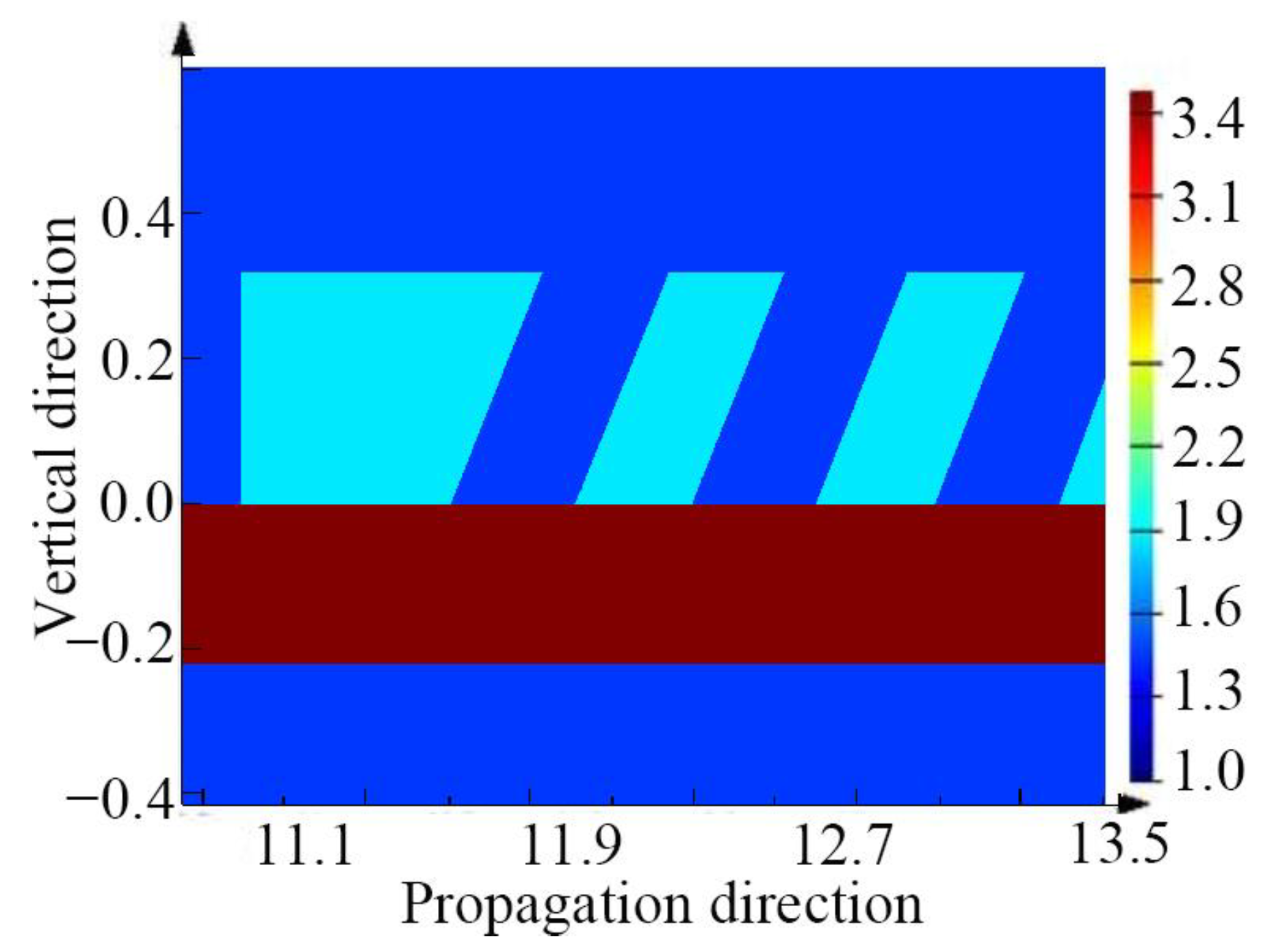
2. Structure
3. Simulation and Discussion
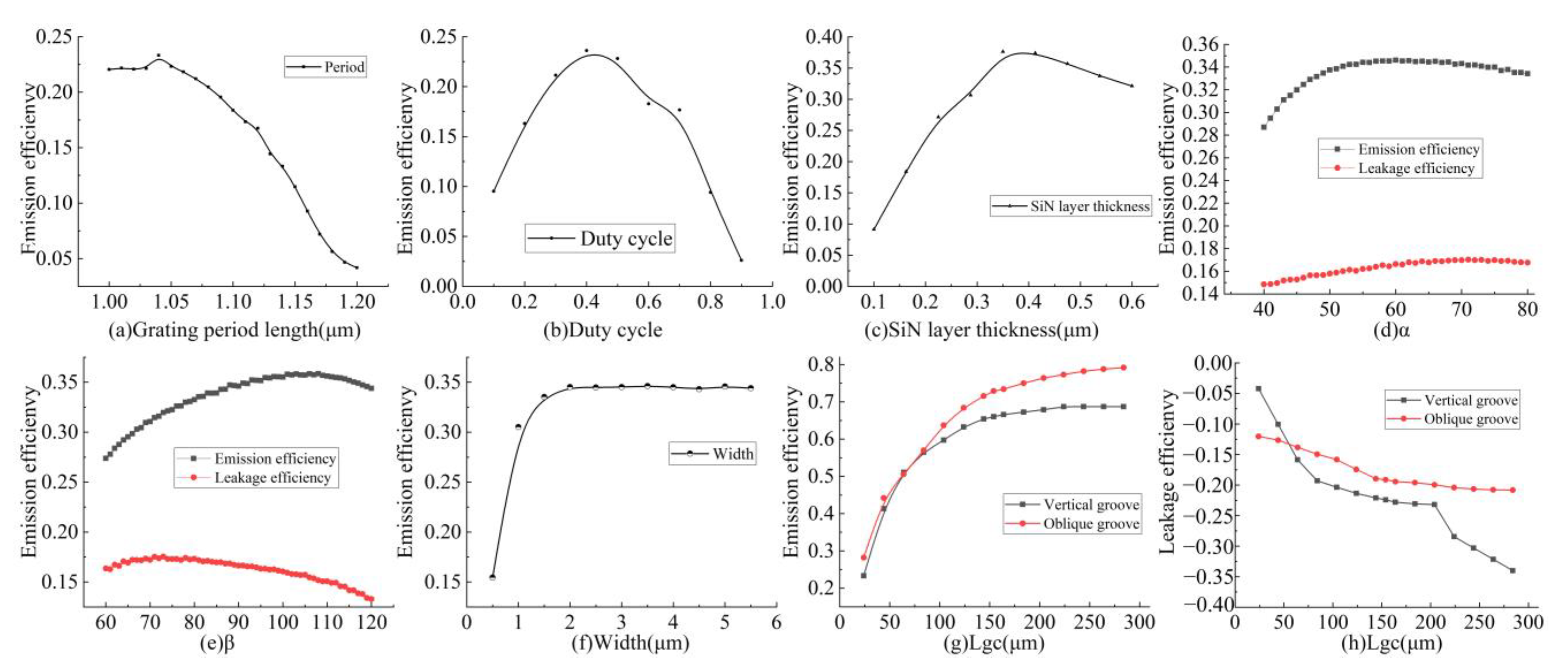
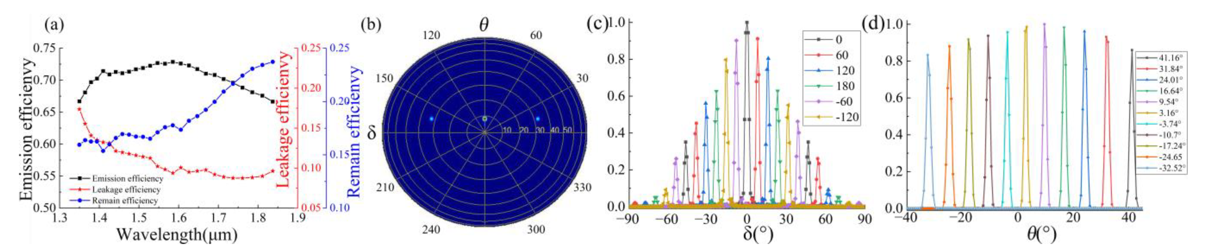
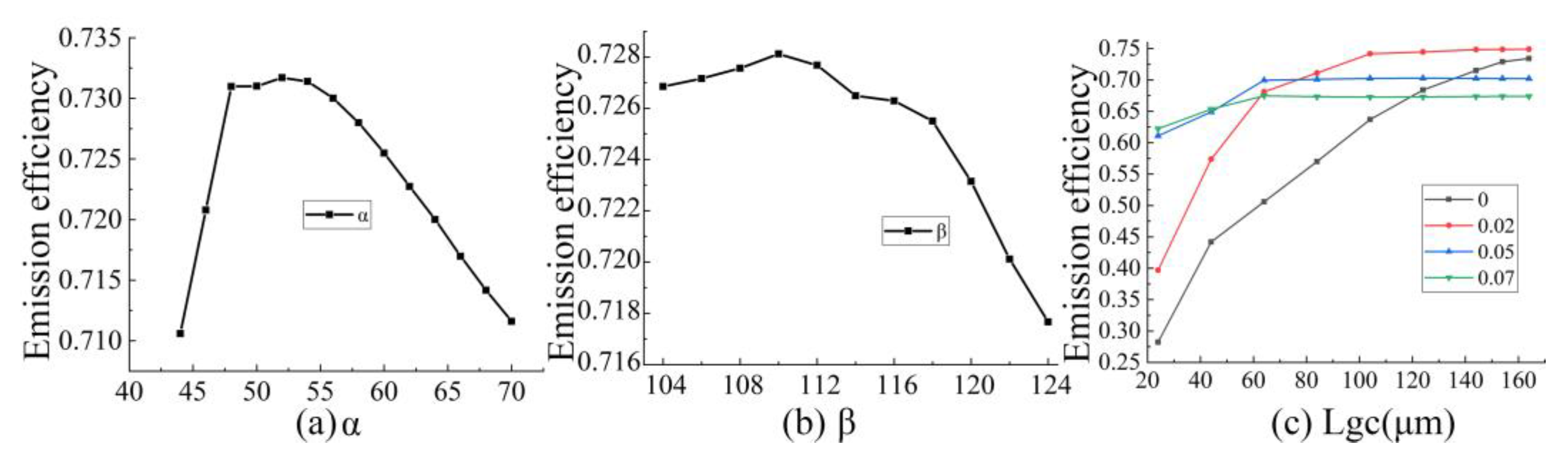
3.1. Antenna Element
3.2. Fabrication Tolerance Analysis and Comparison with Other Work
4. Conclusions
Author Contributions
Funding
Data Availability Statement
Acknowledgments
Conflicts of Interest
References
- Dostart, N.; Zhang, B.; Khilo, A.; Brand, M.; Qubaisi, K.A.; Onural, D.; Feldkhun, D.; Wagner, K.; Popović, A. Serpentine optical phased arrays for scalable integrated photonic LIDAR beam steering. Optica 2020, 7, 726–733. [Google Scholar] [CrossRef]
- Fatemi, R.; Khachaturian, A.; Hajimiri, A. A Nonuniform Sparse 2-D Large-FOV Optical Phased Array With a Low-Power PWM Drive. IEEE J. Solid-State Circuits 2019, 54, 1200–1215. [Google Scholar] [CrossRef]
- Miller, S.A.; Chang, Y.-C.; Phare, C.T.; Shin, M.C.; Zadka, M.; Roberts, S.P.; Stern, B.; Ji, X.; Mohanty, A.; Gordillo, O.A.J.; et al. Large-scale optical phased array using a low-power multi-pass silicon photonic platform. Optica 2020, 7, 3–6. [Google Scholar] [CrossRef]
- Huang, M.C.Y.; Zhou, Y.; Chang-Hasnain, C.J. A surface-emitting laser incorporating a high-index-contrast subwavelength grating. Nat. Photonics 2007, 1, 119–122. [Google Scholar] [CrossRef]
- Roelkens, G.; Vermeulen, D.; Van Laere, F.; Selvaraja, S.; Scheerlinck, S.; Taillaert, D.; Bogaerts, W.; Dumon, P.; Van Thourhout, D.; Baets, R. Bridging the gap between nanophotonic waveguide circuits and single mode optical fibers using diffractive grating structures. J. Nano Nanotechnol. 2010, 10, 1551–1562. [Google Scholar] [CrossRef] [Green Version]
- Zhu, L.; Kapraun, J.; Ferrara, J.; Chang-Hasnain, C. Flexible photonic metastructures for tunable coloration. Optica 2015, 2, 255. [Google Scholar] [CrossRef]
- Zhu, L.; Yang, W.; Chang-Hasnain, C. Very high efficiency optical coupler for silicon nanophotonic waveguide and single mode optical fiber. Opt. Express 2017, 25, 18462–18473. [Google Scholar] [CrossRef]
- Karagodsky, V.; Sedgwick, F.G.; Chang-Hasnain, C.J. Theoretical analysis of subwavelength high contrast grating reflectors. Opt. Express 2010, 18, 16973–16988. [Google Scholar] [CrossRef] [PubMed]
- Poulton, C.V.; Byrd, M.J.; Raval, M.; Su, Z.; Li, N.; Timurdogan, E.; Coolbaugh, D.; Vermeulen, D.; Watts, M.R. Large-scale silicon nitride nanophotonic phased arrays at infrared and visible wavelengths. Opt. Lett. 2017, 42, 21. [Google Scholar] [CrossRef] [PubMed]
- Chung, S.; Abediasl, H.; Hashemi, H. A Monolithically Integrated Large-Scale Optical Phased Array in Silicon-on-Insulator CMOS. IEEE J. Solid-State Circuits 2018, 53, 75–296. [Google Scholar] [CrossRef]
- Doylend, J.K.; Heck, M.J.; Bovington, J.T.; Peters, J.D.; Coldren, L.A.; Bowers, J.E. Two-dimensional free-space beam steering with an optical phased array on silicon-on-insulator. Opt. Express 2011, 19, 21595–21604. [Google Scholar] [CrossRef] [PubMed] [Green Version]
- Van Acoleyen, K.; Komorowska, K.; Bogaerts, W.; Baets, R. One-Dimensional Off-Chip Beam Steering and Shaping Using Optical Phased Arrays on Silicon-on-Insulator. J. Lightwave Technol. 2011, 29, 3500–3505. [Google Scholar] [CrossRef] [Green Version]
- Sun, J.; Timurdogan, E.; Yaacobi, A.; Hosseini, E.S.; Watts, M.R. Large-scale nanophotonic phased array. Nature 2013, 493, 195–199. [Google Scholar] [CrossRef] [PubMed]
- Chang-Hasnain, C.J.; Yang, W. High-contrast gratings for integrated optoelectronics. Adv. Opt. Photonics 2012, 4, 379–440. [Google Scholar] [CrossRef] [Green Version]
- Wang, P.F.; Luo, G.Z.; Yu, H.Y.; Li, Y.J.; Wang, M.Q.; Zhou, X.L.; Chen, W.X.; Zhang, Y.J.; Pan, J.Q. Improving the performance of optical antenna for optical phased arrays through high-contrast grating structure on SOI substrate. Opt. Express 2019, 27, 2703–2712. [Google Scholar] [CrossRef]
- Raval, M.; Poulton, C.V.; Watts, M.R. Unidirectional waveguide grating antennas with uniform emission for optical phased arrays. Opt. Lett. 2017, 42, 2563–2566. [Google Scholar] [CrossRef]
- Ginel-Moreno, P.; Pereira-Martín, D.; Hadij-ElHouati, A.; Ye, W.; Melati, D.; Xu, D.-X.; Janz, S.; Ortega-Moñux, A.; Wangüemert-Pérez, G.; Halir, R.; et al. Highly efficient optical antenna with small beam divergence in silicon waveguides. Opt. Lett. 2020, 45, 5668–5671. [Google Scholar] [CrossRef] [PubMed]
- Khajavi, S.; Melati, D.; Cheben, P.; Schmid, J.H.; Liu, Q.; Xu, D.X.; Ye, W.N. Compact and highly-efficient broadband surface grating antenna on a silicon platform. Opt. Express 2021, 29, 7003–7014. [Google Scholar] [CrossRef] [PubMed]
- Chen, X.; Thomson, D.J.; Crudginton, L.; Khokhar, A.Z.; Reed, G.T. Dual-etch apodised grating couplers for efficient fibre-chip coupling near 1310 nm wavelength. Opt. Express 2017, 25, 17864–17871. [Google Scholar] [CrossRef]
- Yin, X.; Jin, J.; Soljačić, M.; Peng, C.; Zhen, B. Observation of topologically enabled unidirectional guided resonances. Nature 2020, 580, 467–471. [Google Scholar] [CrossRef]
- Cheng, L.; Mao, S.; Li, Z.; Han, Y.; Fu, H.Y. Grating Couplers on Silicon Photonics: Design Principles, Emerging Trends and Practical Issues. Micromachines 2020, 11, 666. [Google Scholar] [CrossRef] [PubMed]
- Schrauwen, J.; Van Laere, F.; Van Thourhout, D.; Baets, R. Focused-ion-beam fabrication of slanted grating couplers in silicon-on-insulator waveguides. IEEE Photonics Technol. Lett. 2007, 19, 816–818. [Google Scholar] [CrossRef] [Green Version]
- Wang, B.; Jiang, J.; Nordin, G.P. Embedded slanted grating for vertical coupling between fibers and silicon-on-insulator planar waveguides. IEEE Photonics Technol. Lett. 2005, 17, 1884–1886. [Google Scholar] [CrossRef]
- Xie, W.; Komljenovic, T.; Huang, J.; Tran, M.; Davenport, M.; Torres, A.; Pintus, P.; Bowers, J. Heterogeneous silicon photonics sensing for autonomous cars [Invited]. Opt. Express 2019, 27, 3642–3663. [Google Scholar] [CrossRef]
- Vogt, M.R. Development of physical models for the simulation of optical properties of solar cell modules. Tech. Inf. (TIB) 2016, 3, 37. [Google Scholar]
- Chrostowski, L.; Hochberg, M. Silicon Photonics Design: From Devices to Systems; Cambridge University Press: Cambridge, UK, 2015. [Google Scholar] [CrossRef]
- Doerr, C.R.; Chen, L.; Chen, Y.; Buhl, L.L. Wide Bandwidth Silicon Nitride Grating Coupler. IEEE Photonics Technol. Lett. 2010, 22, 1461–1463. [Google Scholar] [CrossRef]
- Zhang, Z.; Kleinert, M.; Maese-Novo, A.; Irmscher, G.; Schwartz, E.; Zawadzki, C.; Keil, N. Multicore polymer waveguides and multistep 45 mirrors for 3D photonic integration. IEEE Photonics Technol. Lett. 2014, 26, 1986–1989. [Google Scholar] [CrossRef]
- Lee, J.K.; Lee, S.H.; Min, J.H.; Jang, I.Y.; Kim, C.K.; Moonet, S.H. Oblique-directional plasma etching of Si using a Faraday cage. J. Electrochem. Soc. 2009, 156, D222. [Google Scholar] [CrossRef]
- Stegmuller, B.; Westermeier, H.; Thulke, W.; Franz, G.; Sacher, D. Surface emitting InGaAsP/InP distributed feedback laser diode at 1.53 mu m with monolithic integrated microlens. IEEE Photonics Technol. Lett. 1991, 3, 776–778. [Google Scholar] [CrossRef]
- Boyd, G.D.; Coldren, L.A.; Storz, F.G. Directional reactive ion etching at oblique angles. Appl. Phys. Lett. 1980, 36, 583–585. [Google Scholar] [CrossRef]
- Schaepkens, M.; Oehrlein, G.S. A review of SiO2 etching studies in inductively coupled fluorocarbon plasmas. J. Electrochem. Soc. 2001, 148, C211. [Google Scholar] [CrossRef]
- Sheen, D.M.; Ali, S.M.; Abouzahra, M.D.; Kong, J.A. Application of the three-dimensional finite-difference time-domain method to the analysis of planar microstrip circuits. IEEE Trans. Microw. Theory Tech. 1990, 38, 849–857. [Google Scholar] [CrossRef]
- Oetting, C.C.; Klinkenbusch, L. Near-to-Far-Field Transformation by a Time-Domain Spherical-Multipole Analysis. IEEE Trans. Antennas Propag. 2005, 53, 2054–2063. [Google Scholar] [CrossRef]

| Name | Meaning | Result |
|---|---|---|
| Lgc (μM) | Grating area length | 150 |
| Wgc (μM) | Grating area width | 2 |
| α° | Inclination1 | 55 |
| β° | Inclination2 | 110 |
| (μM) | Grating period | 1.04 |
| Dc | Grating duty cycle | 0.4 |
| SiN thickness (μM) | SiN layer thickness | 0.35 |
| LTaper (μM) | Taper length | 11 |
| Element Size | Working Bandwidth | Emission Efficiency (At Center Working Wavelength) | |
|---|---|---|---|
| This work | 2 μM × 150 μM | 500 nm (1 dB) | 73% |
| CN (2021) [18] | 7.6 μM × 4.5 μM | 230 nm (1 dB) | 89% |
| NRCS (2020) [17] | 3.65 mm | N.A. | 72% |
| UCAS (2019) [15] | 1.5 μM × 80 μM | 140 nm (3 dB) | 94% |
| MIT (2017) [16] | 3 mm | N.A. | 93% |
| MIT (2013) [13] | 9 μM × 9 μM | N.A. | 51% |
Publisher’s Note: MDPI stays neutral with regard to jurisdictional claims in published maps and institutional affiliations. |
© 2021 by the authors. Licensee MDPI, Basel, Switzerland. This article is an open access article distributed under the terms and conditions of the Creative Commons Attribution (CC BY) license (https://creativecommons.org/licenses/by/4.0/).
Share and Cite
Wang, Z.; Liao, J.; Xie, Y.; Sun, Y.; Li, X.; Li, W. High-Efficiency, Wide Working Bandwidth Antenna Based on SOI Platform for Optical Phased Array. Micromachines 2021, 12, 996. https://doi.org/10.3390/mi12080996
Wang Z, Liao J, Xie Y, Sun Y, Li X, Li W. High-Efficiency, Wide Working Bandwidth Antenna Based on SOI Platform for Optical Phased Array. Micromachines. 2021; 12(8):996. https://doi.org/10.3390/mi12080996
Chicago/Turabian StyleWang, Zihao, Jiali Liao, Yixiang Xie, Yanling Sun, Xifeng Li, and Wei Li. 2021. "High-Efficiency, Wide Working Bandwidth Antenna Based on SOI Platform for Optical Phased Array" Micromachines 12, no. 8: 996. https://doi.org/10.3390/mi12080996
APA StyleWang, Z., Liao, J., Xie, Y., Sun, Y., Li, X., & Li, W. (2021). High-Efficiency, Wide Working Bandwidth Antenna Based on SOI Platform for Optical Phased Array. Micromachines, 12(8), 996. https://doi.org/10.3390/mi12080996