
Evaluation of Self-Field Effects in Magnetometers Based on Meander-Shaped Arrays of Josephson Junctions or SQUIDs Connected in Series †

 , , and
Abstract
:1. Introduction
2. Ideal Devices
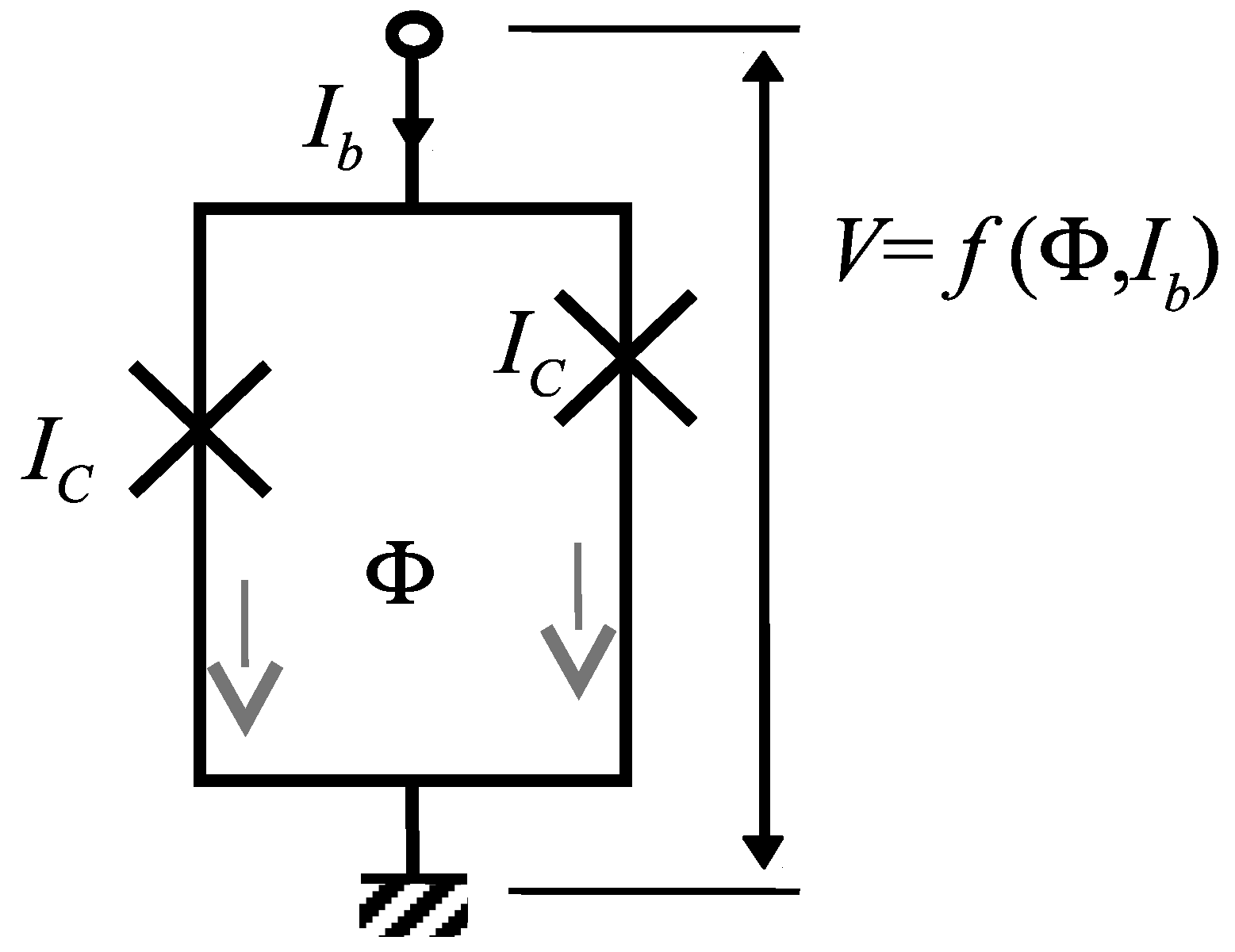
2.1. Single SQUID
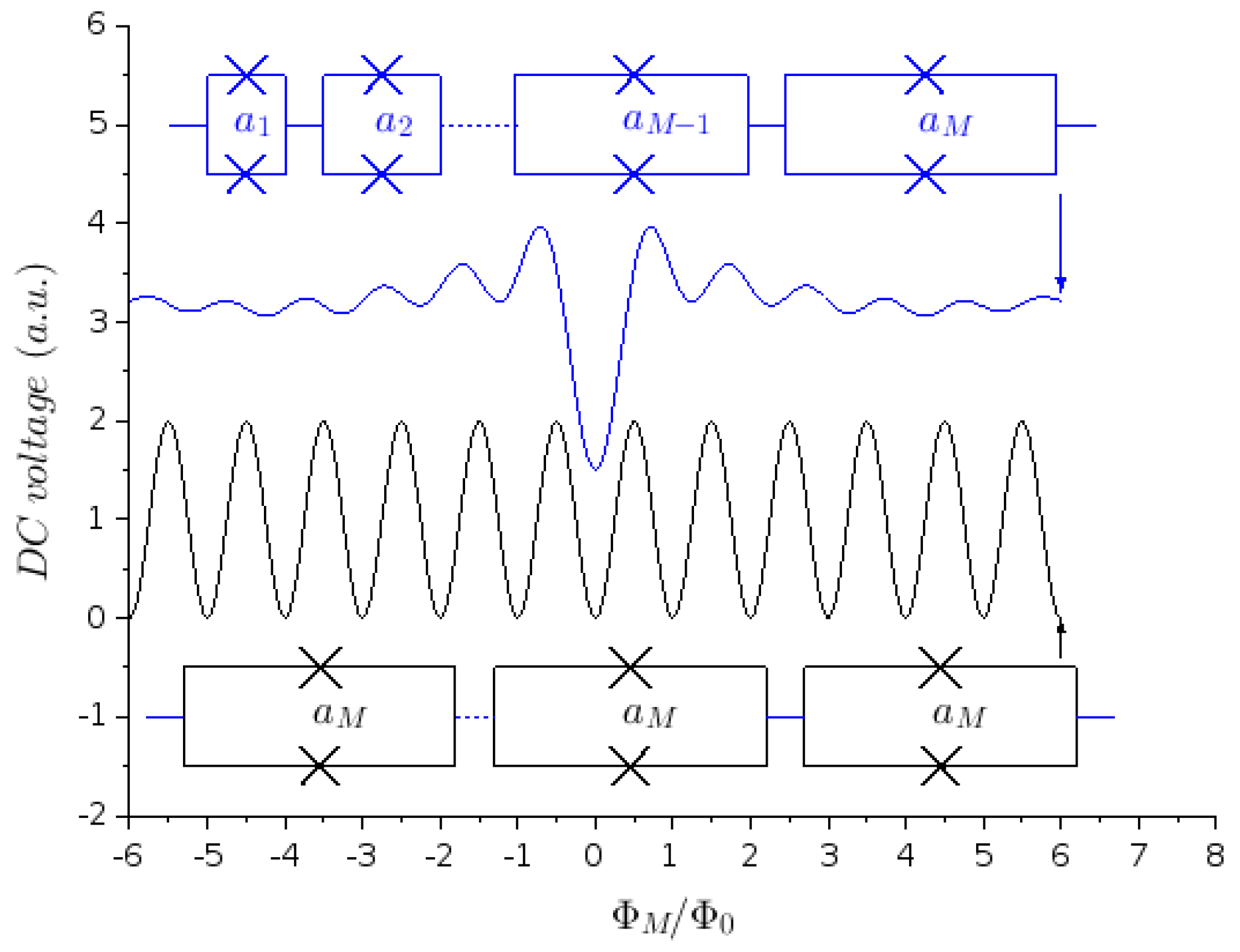
2.2. Arrays of Josephson Junctions
- the input noise spectral density (NSD) , assuming that the SQUID noise contributions are not correlated;
- the spur-free dynamic range (SFDR);
- and the dynamic range, as the output noise is independent of N.
3. Self-Flux
3.1. Origin
3.2. Layout Asymmetry
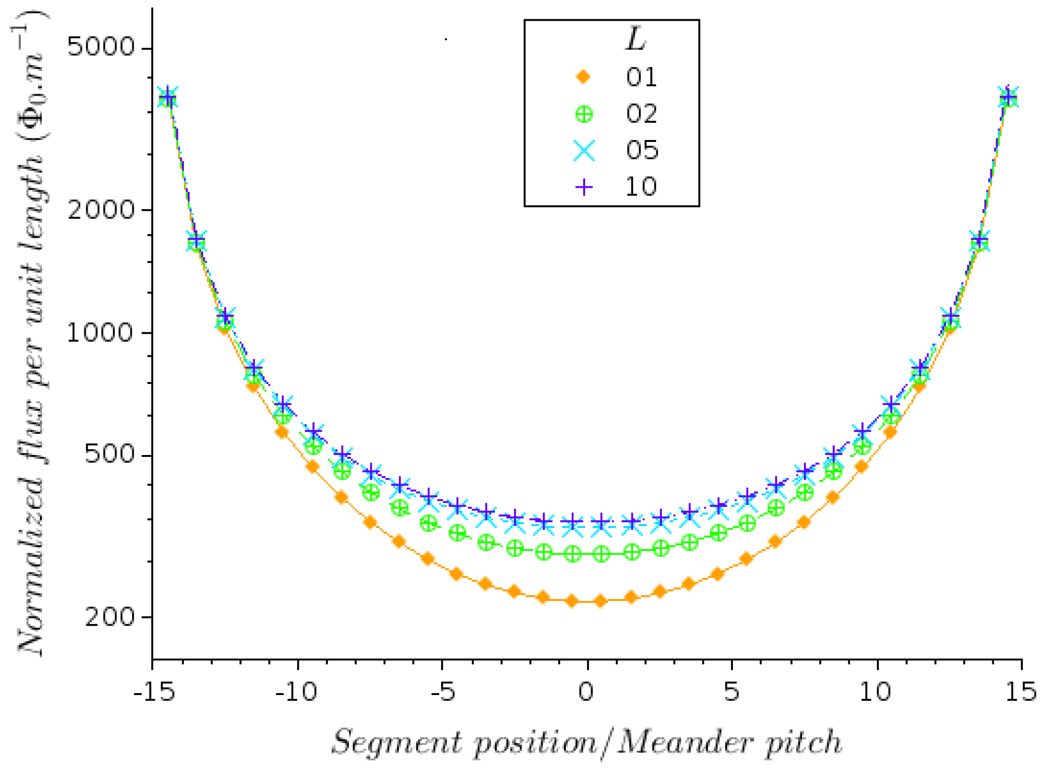
3.3. Evaluation of Self-Flux in a Meander Arrangement
3.4. Josephson Asymmetry
4. Evaluation of Self-Flux Degradation on the Array Performance
4.1. Impact of Layout
4.2. Impact of Scattering
5. Compensation
- it is necessary to keep small to maintain the modulation amplitude of individual SQUIDs;
- smaller SQUIDs are less sensitive to “inter-SQUID” self-flux;
- and, as seen in Section 4.2, they are less sensitive to “intra-SQUID” self-flux.
- increasing the impedance of the readout electronics, which is possible only for low-frequency devices because it reduces the bandwidth of the system;
- associating devices in parallel to lower its output impedance;
- and using flux transformers and/or flux concentrators [39].
6. Josephson Junction Series Arrays
7. Discussion
8. Conclusions
9. Patents
Author Contributions
Funding
Institutional Review Board Statement
Informed Consent Statement
Data Availability Statement
Conflicts of Interest
Abbreviations
| JJ | Josephson junction |
| JSA | Josephson junction series array |
| LJJ | Long Josephson junction |
| NSD | Noise spectral density |
| SFDR | Spur-free dynamic range |
| SNR | Signal-to-noise ratio |
| SQUID | Superconducting quantum interference device |
| SSA | SQUID series array |
| WPD | Superconducting wave functions phase difference |
References
- Forgacs, R.L.; Warnick, A. Lock-On Magnetometer Utilizing a Superconducting Sensor. IEEE Trans. Instr. Meas. 1966, 3, 113–120. [Google Scholar] [CrossRef]
- Drung, D. High-Tc and Low-Tc dc SQUID Electronics. Supercond. Sci. Technol. 2003, 16, 1320–1336. [Google Scholar] [CrossRef]
- Clarke, J.; Hawkins, G. Flicker (l/f) noise in Josephson tunnel junctions. Phys. Rev. B 1976, 14, 2826. [Google Scholar] [CrossRef] [Green Version]
- Clarke, J. Superconducting quantum interference devices for low frequency measurements. In Superconductor Applications: SQUIDs and Machines; Schwartz, B.B., Foner, S., Eds.; Plenum: New York, NY, USA, 1977. [Google Scholar]
- Clarke, J. Advances in SQUID magnetometers. IEEE Trans. Elect. Dev. 1980, ED-27, l896. [Google Scholar] [CrossRef] [Green Version]
- Storm, J.-H.; Hömmen, P.; Drung, D.; Körber, R. An ultra-sensitive and wideband magnetometer based on a superconducting quantum interference device. Appl. Phys. Lett. 2017, 110, 072603. [Google Scholar] [CrossRef] [Green Version]
- Schmelz, M.; Stolz, R.; Zakosarenko, V.; Schonau, T.; Anders, S.; Fritzsch, L.; Muck, M.; Meyer, H.-G. Field-stable SQUID magnetometer with sub-fT.Hz−1/2 resolution based on sub-micrometer cross-type Josephson tunnel junctions. Supercond. Sci. Technol. 2011, 24, 065009. [Google Scholar]
- Faley, M.I.; Poppe, U.; Urban, K.; Slobodchikov, V.Y.; Maslennikov, Y.V.; Gapelyuk, A.; Sawitzki, B.; Schirdewan, A. Operation of high-temperature superconductor magnetometer with submicrometer bicrystal junctions. Appl. Phys. Lett. 2002, 81, 1323. [Google Scholar] [CrossRef] [Green Version]
- Dong, H.; Zhang, Y.; Krause, H.-J.; Xie, X.; Offenhausser, A. Low Field MRI Detection With Tuned HTS SQUID Magnetometer. IEEE Trans. Appl. Supercond. 2011, 21, 509–513. [Google Scholar] [CrossRef]
- Enpuku, K.; Hirakawa, S.; Tsuji, Y.; Momotomi, R.; Matsuo, M.; Yoshida, T.; Kandori, A. HTS SQUID Magnetometer Using Resonant Coupling of Cooled Cu Pickup Coil. IEEE Trans. Appl. Supercond. 2011, 21, 514–517. [Google Scholar] [CrossRef]
- Adachi, S.; Tsukamoto, A.; Hato, T.; Kawano, J.; Tanabe, K. Recent development of high-Tc electronic devices with multilayer structures and ramp-edge Josephson junctions. IEICE Trans. Electron. 2012, 95, 337–346. [Google Scholar] [CrossRef] [Green Version]
- Faley, M.; Dammers, J.; Maslennikov, Y.; Schneiderman, J.; Winkler, D.; Koshelets, V.; Shah, N.; Dunin-Borkowski, R. High-Tc SQUID biomagnetometers. Supercond. Sci. Technol. 2017, 30, 083001. [Google Scholar] [CrossRef]
- Trabaldo, E.; Pfeiffer, C.; Andersson, E.; Arpaia, R.; Kalaboukhov, A.; Winkler, D.; Lombardi, F.; Bauch, T. Grooved Dayem Nanobridges as Building Blocks of High-Performance YBa2Cu3O7δ SQUID Magnetometers. Nano Lett. 2019, 19, 1902–1907. [Google Scholar] [CrossRef] [Green Version]
- Trabaldo, E.; Pfeiffer, C.; Andersson, E.; Arpaia, R.; Kalaboukhov, A.; Winkler, D.; Lombardi, F.; Bauch, T. SQUID magnetometer based on Grooved Dayem nanobridges and a flux transformer. Appl. Phys. Lett. 2020, 116, 132601. [Google Scholar] [CrossRef]
- Prêle, D.; Piat, M.; Sipile, L.; Voisin, F. Operating Point and Flux Jumps of a SQUID in Flux-Locked Loop. IEEE Trans. Appl. Supercond. 2016, 26, 2. [Google Scholar] [CrossRef]
- Schönau, T.; Schmelz, M.; Zakosarenko, V.; Stolz, R.; Meyer, M.; Anders, S.; Fritzsch, L.; Meyer, H.-G. SQUID-based setup for the absolute measurement of the Earth’s magnetic field. Supercond. Sci. Technol. 2013, 26, 035013. [Google Scholar] [CrossRef]
- Drung, D.; Aßmann, C.; Beyer, J.; Kirste, A.; Peters, M.; Ruede, F.; Schurig, T. Highly sensitive and easy-to-use SQUID sensors. IEEE Trans. Appl. Supercond. 2007, 17, 699–704. [Google Scholar] [CrossRef]
- Foglietti, V. Double dc SQUID for flux-locked-loop operation. Appl. Phys. Lett. 1991, 59, 476. [Google Scholar] [CrossRef]
- Prokopenko, G.V.; Shitov, S.V.; Lapitskaya, I.L.; Koshelets, V.P.; Mygind, J. Dynamic characteristics of S-band DC SQUID amplifier. IEEE Trans. Appl. Supercond. 2003, 13, 1048. [Google Scholar] [CrossRef] [Green Version]
- Mück, M.; McDermott, R. Radio-frequency amplifiers based on dcSQUIDs. Supercond. Sci. Technol. 2010, 23, 093001. [Google Scholar] [CrossRef]
- Feynman, R.P.; Leighton, R.B.; Sands, M. The Feynman Lectures on Physics; Addison-Wesley: Reading, MA, USA, 1966. [Google Scholar]
- Welty, R.P.; Martinis, J.M. A Series Array of DC SQUIDs. IEEE Trans. Mag. 1991, 27, 2924–2926. [Google Scholar] [CrossRef]
- Häussler, C.; Oppenländer, J.; Schopohl, N. Nonperiodic Flux to Voltage Conversion of Series Arrays of dc Superconducting Quantum Interference Devices. J. Appl. Phys. 2001, 89, 1875–1879. [Google Scholar] [CrossRef] [Green Version]
- Carelli, P.; Castellano, M.G.; Flacco, K.; Leoni, R.; Torrioli, G. An Absolute Magnetometer Based on dc Superconducting QUantum Interference Devices. Europhys. Lett. 1997, 39, 569–574. [Google Scholar] [CrossRef]
- Cybart, S.A.; Herr, A.; Kornev, V.; Foley, C.P. Do multiple Josephson junctions make better devices? Supercond. Sci. Technol. 2017, 30, 090201. [Google Scholar] [CrossRef]
- LeFebvre, J.C.; Cho, E.; Li, H.; Pratt, K.; Cybart, S.A. Series Arrays of Planar Long Josephson Junctions for High Dynamic Range Magnetic Flux Detection. AIP Adv. 2019, 9, 105215. [Google Scholar] [CrossRef]
- Josephson, B.D. Possible New Effects in Superconductive Tunnelling. Phys. Lett. 1962, 1, 251–253. [Google Scholar] [CrossRef]
- Cybart, S.; Cho, E.; Wong, T.; Wehlin, B.; Ma, M.; Huynh, C.; Dynes, R. Nano Josephson superconducting tunnel junctions in YBa2Cu3O7δ directly patterned with a focused helium ion beam. Nat. Nanotechnol. 2015, 10, 598. [Google Scholar] [CrossRef]
- Kornev, V.; Kolotinskiy, N.; Skripka, V.; Sharafiev, A.; Soloviev, I.; Mukhanov, O. High Linearity Voltage Response Parallel-Array Cell. J. Phys. Conf. Ser. 2014, 507, 042018. [Google Scholar] [CrossRef] [Green Version]
- Mitchell, E.E.; Müller, K.-H.; Purches, W.E.; Keenan, S.T.; Lewis, C.J.; Foley, C.P. Quantum interference effects in 1D parallel high-Tc SQUID arrays with finite inductance. Supercond. Sci. Technol. 2019, 32, 124002. [Google Scholar] [CrossRef]
- Mitchell, E.E.; Hannam, K.E.; Lazar, J.; Leslie, K.E.; Lewis, C.J.; Grancea, A.; Keenan, S.T.; Lam, S.K.H.; Foley, C.P. 2D SQIF arrays using 20,000 YBCO high RN Josephson junctions. Supercond. Sci. Tech. 2016, 29, 06LT01. [Google Scholar] [CrossRef]
- Tesche, C.; Clarke, J. DC SQUID: Noise and Optimization. J. Low. Temp. Phys. 1977, 29, 301–331. [Google Scholar] [CrossRef]
- Chesca, B.; Kleiner, R.; Koelle, D. SQUID Theory. In The SQUID Handbook 1; Clarke, J., Braginski, A.I., Eds.; Wiley-VCH: Wienheim, Germany, 2004; pp. 65–69. [Google Scholar]
- Crété, D.; Sène, A.; Labbé, A.; Recoba Pawlowski, E.; Kermorvant, J.; Lemaître, Y.; Marcilhac, B.; Parzy, E.; Thiaudière, E.; Ulysse, C. Evaluation of Josephson Junction Parameter Dispersion Effects in Arrays of HTS SQUIDs. IEEE Trans. Appl. Supercond. 2018, 28, 1602506. [Google Scholar] [CrossRef]
- InductEx. Available online: http://www0.sun.ac.za/ix/ (accessed on 15 November 2021).
- Enpuku, K.; Tokita, G.; Maruo, T.; Minotani, T. Parameter dependencies of characteristics of a high-Tc dc superconducting quantum interference device. J. Appl. Phys. 1995, 78, 3498–3503. [Google Scholar] [CrossRef]
- Crété, D.; Lemaître, Y.; Trastoy, J.; Marcilhac, B.; Ulysse, C. Integration Density of Ion-Damaged Barrier Josephson Junction and Circuits. J. Phys. Conf. Ser. 2019, 1182, 1. [Google Scholar] [CrossRef]
- Crété, D.; Lemaître, Y.; Marcilhac, B.; Recoba-Pawlowski, E.; Trastoy, J.; Ulysse, C. Optimal SQUID Loop Size in Arrays of HTS SQUIDs. J. Phys. Conf. Ser. 2020, 1559, 012012. [Google Scholar] [CrossRef]
- Labbé, A.; Parzy, E.; Thiaudière, E.; Massot, P.; Franconi, J.-M.; Ulysse, C.; Lemaître, Y.; Marcilhac, B.; Crété, D.; Kermorvant, J. Effects of Flux Pinning on the DC Characteristics of Meander-Shaped Superconducting Quantum Interference Filters with Flux Concentrator. J. Appl. Phys. 2018, 124, 214503. [Google Scholar] [CrossRef]
- Fiske, M.D. Temperature and Magnetic Field Dependences of the Josephson Tunneling Current. Rev. Mod. Phys. 1964, 36, 221–222. [Google Scholar] [CrossRef]
- Owen, C.S.; Scalapino, D.J. Vortex Structure and Critical Currents in Josephson Junctions. Phys. Rev. 1967, 164, 538. [Google Scholar] [CrossRef]
- Dolabdjian, C.; Poupard, P.; Martin, V.; Gunther, C.; Hamet, J.F.; Robbes, D. A linearized Josephson—Fraunhofer magnetometer with high-temperature Josephson junction. Rev. Scien. Instrum. 1996, 67, 4171. [Google Scholar] [CrossRef]
- Golod, T.; Kapran, O.M.; Krasnov, V.M. Planar Superconductor-Ferromagnet-Superconductor Josephson Junctions as Scanning-Probe Sensors. Phys. Rev. Appl. 2019, 11, 014062. [Google Scholar] [CrossRef] [Green Version]
- Rosenthal, P.A.; Beasley, M.; Char, K.; Colclough, M.; Zaharchuk, G. Flux Focusing Effects in Planar Thin-Film Grain-Boundary Josephson Junctions. Appl. Phys. Lett. 1991, 59, 3482–3484. [Google Scholar] [CrossRef]
- Bergeal, N.; Grison, X.; Lesueur, J.; Faini, G.; Aprili, M.; Contour, J.P. High-Quality Planar High-Tc Josephson Junctions. Appl. Phys. Lett. 2005, 87, 102502. [Google Scholar] [CrossRef] [Green Version]
- Monaco, R.; Granata, C.; Russo, R.; Vettoliere, A. Ultra-Low-Noise Magnetic Sensing with Long Josephson Tunnel Junctions. Supercond. Sci. Tech. 2013, 26, 125005. [Google Scholar] [CrossRef]


| Arrangement | Series | Parallel | 2D |
|---|---|---|---|
| Modulation | N | 1 | N |
| Transfer Factor | N | 1 | N |
| Impedance | N | ||
| Output Signal Power | N | M | |
| Output NSD | N | ||
| Output Noise Power | 1 | 1 | 1 |
| Input NSD | |||
| SFDR |
Publisher’s Note: MDPI stays neutral with regard to jurisdictional claims in published maps and institutional affiliations. |
© 2021 by the authors. Licensee MDPI, Basel, Switzerland. This article is an open access article distributed under the terms and conditions of the Creative Commons Attribution (CC BY) license (https://creativecommons.org/licenses/by/4.0/).
Share and Cite
Crété, D.; Kermorvant, J.; Lemaître, Y.; Marcilhac, B.; Mesoraca, S.; Trastoy, J.; Ulysse, C. Evaluation of Self-Field Effects in Magnetometers Based on Meander-Shaped Arrays of Josephson Junctions or SQUIDs Connected in Series. Micromachines 2021, 12, 1588. https://doi.org/10.3390/mi12121588
Crété D, Kermorvant J, Lemaître Y, Marcilhac B, Mesoraca S, Trastoy J, Ulysse C. Evaluation of Self-Field Effects in Magnetometers Based on Meander-Shaped Arrays of Josephson Junctions or SQUIDs Connected in Series. Micromachines. 2021; 12(12):1588. https://doi.org/10.3390/mi12121588
Chicago/Turabian StyleCrété, Denis, Julien Kermorvant, Yves Lemaître, Bruno Marcilhac, Salvatore Mesoraca, Juan Trastoy, and Christian Ulysse. 2021. "Evaluation of Self-Field Effects in Magnetometers Based on Meander-Shaped Arrays of Josephson Junctions or SQUIDs Connected in Series" Micromachines 12, no. 12: 1588. https://doi.org/10.3390/mi12121588
APA StyleCrété, D., Kermorvant, J., Lemaître, Y., Marcilhac, B., Mesoraca, S., Trastoy, J., & Ulysse, C. (2021). Evaluation of Self-Field Effects in Magnetometers Based on Meander-Shaped Arrays of Josephson Junctions or SQUIDs Connected in Series. Micromachines, 12(12), 1588. https://doi.org/10.3390/mi12121588