
Design and Fabrication of Double-Layer Crossed Si Microchannel Structure


Abstract
:1. Introduction
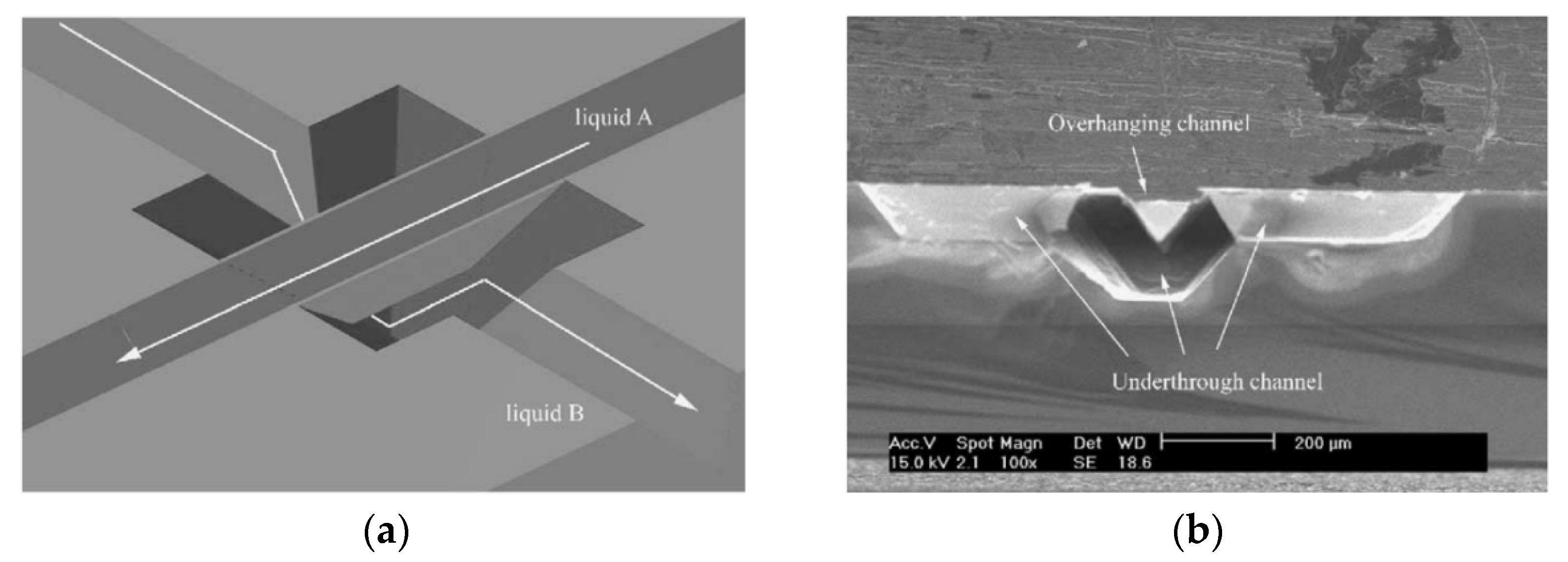
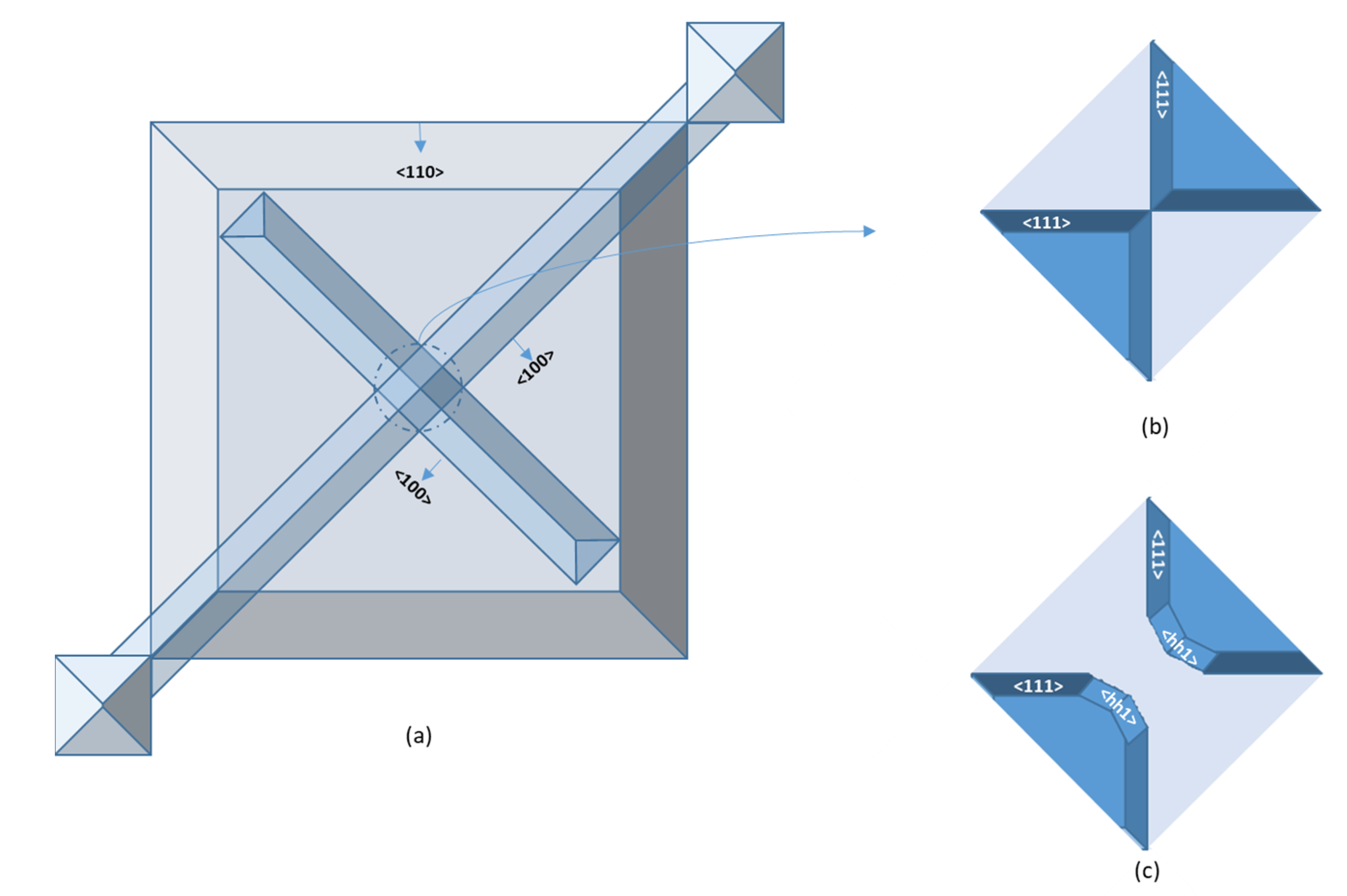
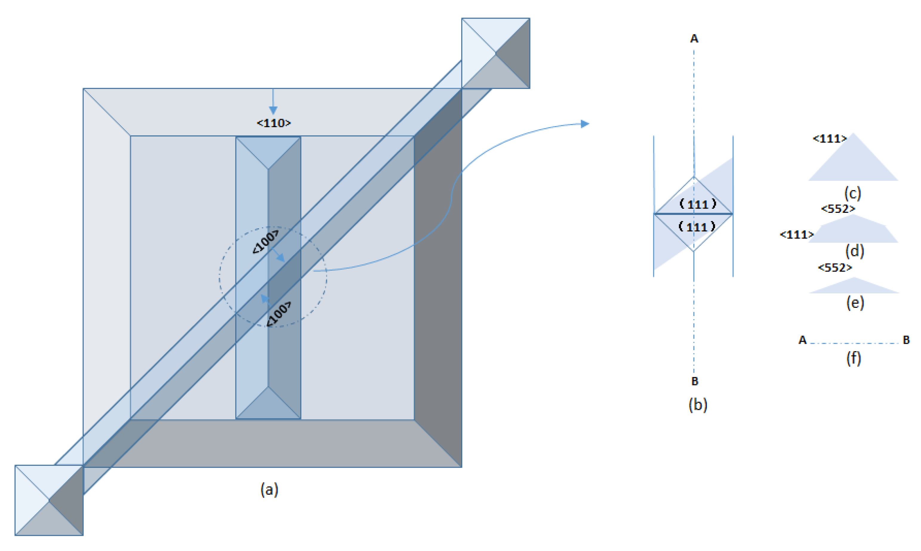
2. Design
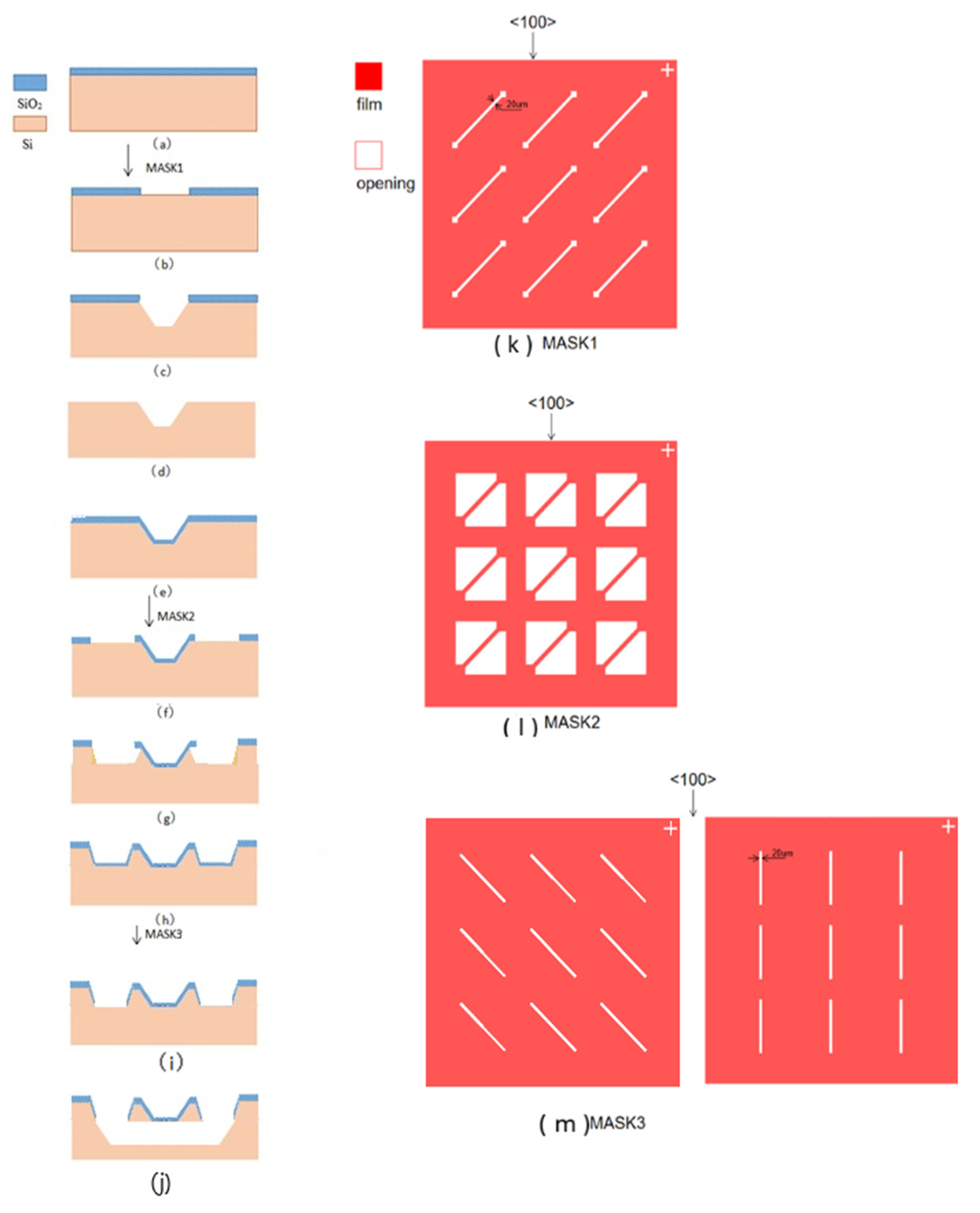
3. Experimental Procedure
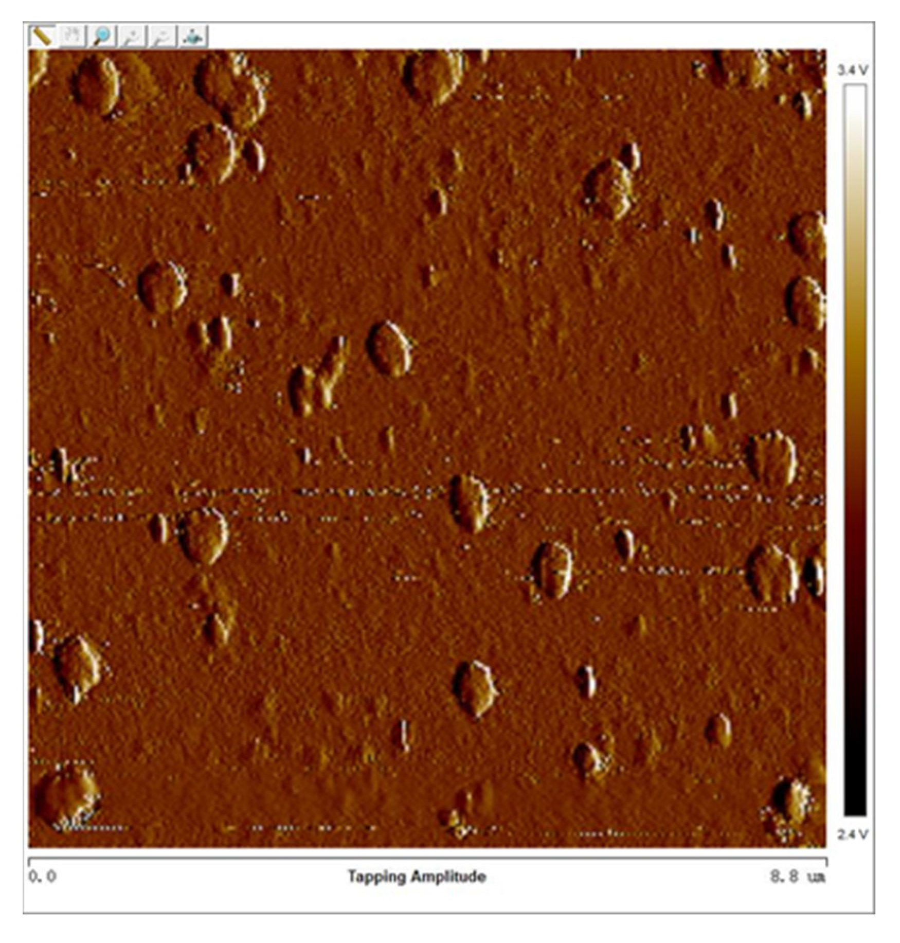
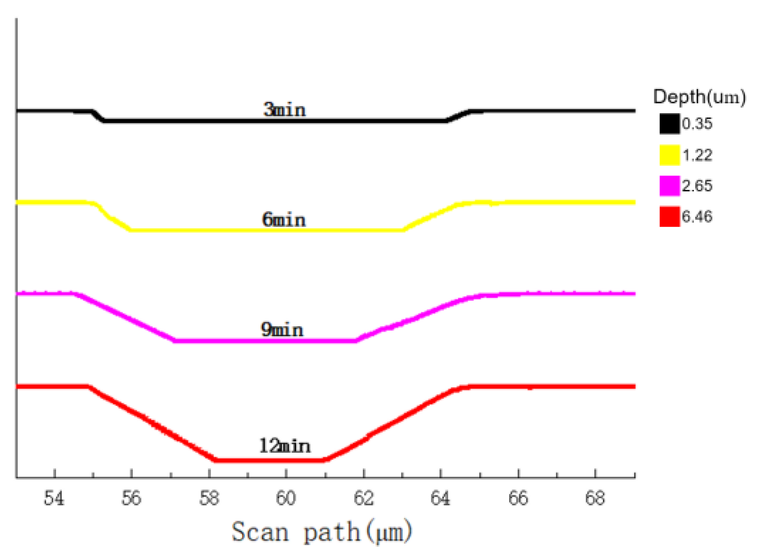
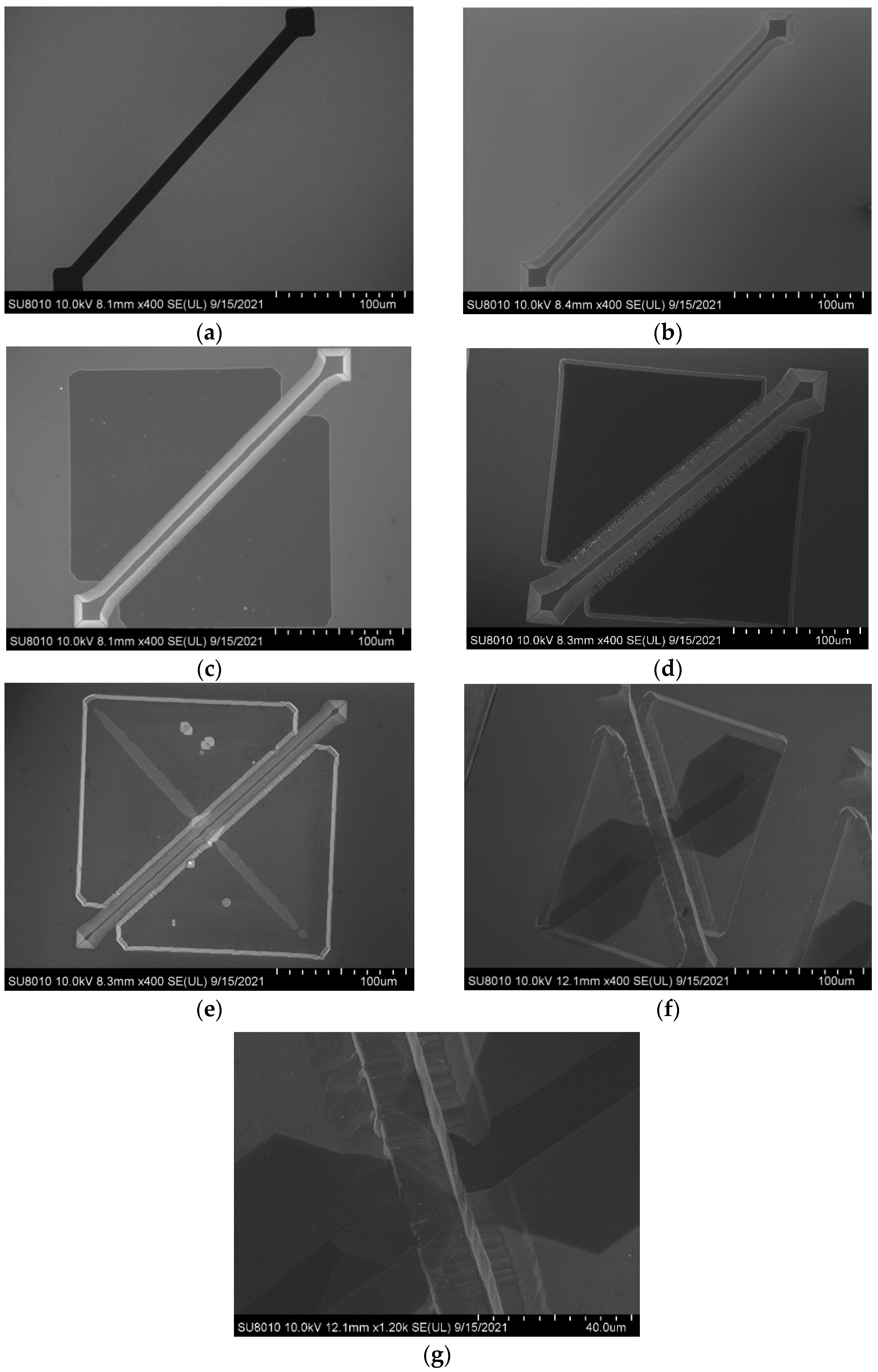
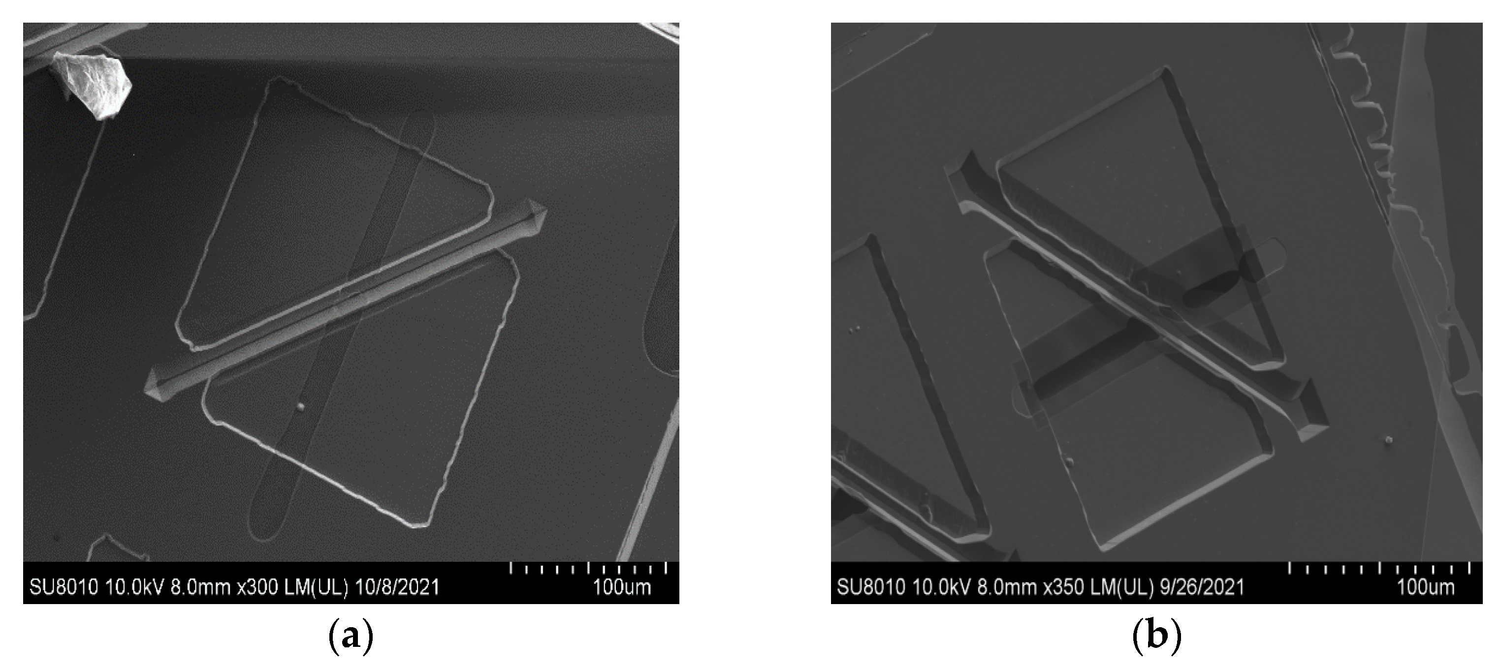
4. Results and Discussion
5. Conclusions
Author Contributions
Funding
Institutional Review Board Statement
Informed Consent Statement
Conflicts of Interest
References
- Roos, M.M.; Winkler, A.; Nilsen, M.; Menzel, S.B.; Strehle, S. Towards Green 3D-Microfabrication of Bio-MEMS Devices Using ADEX Dry Film Photoresists. Int. J. Precis. Eng. Manuf.-Green Technol. 2021, 8, 1536. [Google Scholar] [CrossRef]
- Kamat, A.M.; Pei, Y.; Jayawardhana, B.; Kottapalli, A.G.P. Biomimetic Soft Polymer Microstructures and Piezoresistive Graphene MEMS Sensors Using Sacrificial Metal 3D Printing. ACS Appl. Mater. Interfaces 2021, 13, 1094–1104. [Google Scholar] [CrossRef]
- Velden, G.; Fan, D.; Staufer, U. Fabrication of a microfluidic device by using two-photon lithography on a positive photoresist. Micro Nano Eng. 2020, 7, 100054. [Google Scholar] [CrossRef]
- Kaltsas, G.; Pagonis, D.N.; Nassiopoulou, A.G. Planar CMOS compatible process for the fabrication of buried microchannels in Si using porous Si technology. J. Microelectromech. Syst. 2004, 12, 863–872. [Google Scholar] [CrossRef]
- Ahmed, H.; Ramesan, S.; Lee, L.; Rezk, A.R.; Yeo, L.Y. On-Chip Generation of Vortical Flows for Microfluidic Centrifugation. Small 2020, 16, 1903605. [Google Scholar] [CrossRef]
- Jasińska, L.; Malecha, K. Microfluidic Modules Integrated with Microwave Components—Overview of Applications from the Perspective of Different Manufacturing Technologies. Sensors 2021, 21, 1710. [Google Scholar] [CrossRef] [PubMed]
- Xu, X.; Huang, X.; Sun, J.; Wang, R.; Yao, J.; Han, W.; Wei, M.; Chen, J.; Guo, J.; Sun, L.; et al. Recent progress of inertial microfluidic-based cell separation. Analyst 2021, 23, 146. [Google Scholar] [CrossRef]
- Fatehifar, M.; Revell, A.; Jabbari, M. Non-Newtonian Droplet Generation in a Cross-Junction Microfluidic Channel. Polymers 2021, 13, 1915. [Google Scholar] [CrossRef] [PubMed]
- Chung, Y.C.; Chung, H.H.; Lin, S.H. Improvement of Temperature and Optical Power of an LED by Using Microfluidic Circulating System of Graphene Solution. Nanomaterials 2021, 11, 1719. [Google Scholar] [CrossRef]
- Yuan, C.; Zhang, H.; Li, X.; Oishi, M.; Oshima, M.; Yao, Q.; Li, F. Numerical Investigation of T-Shaped Microfluidic Oscillator with Viscoelastic Fluid. Micromachines 2021, 12, 477. [Google Scholar] [CrossRef] [PubMed]
- Fallahi, H.; Zhang, J.; Phan, H.P.; Nguyen, N.T. Flexible Microfluidics: Fundamentals, Recent Developments, and Applications. Micromachines 2019, 10, 830. [Google Scholar] [CrossRef] [Green Version]
- Cai, G.; Xue, L.; Zhang, H.; Lin, J. A Review on Micromixers. Micromachines 2017, 8, 274. [Google Scholar] [CrossRef]
- Liu, C.; Hu, G. High-Throughput Particle Manipulation Based on Hydrodynamic Effects in Microchannels. Micromachines 2017, 8, 73. [Google Scholar] [CrossRef] [Green Version]
- Pattanayak, P.; Singh, S.K.; Gulati, M.; Vishwas, S.; Kapoor, B.; Chellappan, D.K.; Anand, K.; Gupta, G.; Jha, N.K.; Gupta, P.K.; et al. Microfluidic chips: Recent advances, critical strategies in design, applications and future perspectives. Microfluid. Nanofluidics 2021, 25, 1–28. [Google Scholar] [CrossRef] [PubMed]
- Zhang, J.; Yan, S.; Yuan, D.; Alici, G.; Nguyen, N.T.; Warkiani, M.E.; Li, W. Fundamentals and Applications of Inertial Microfluidics: A Review. Lab Chip 2015, 16, 10–34. [Google Scholar] [CrossRef] [Green Version]
- Cubaud, T.; Mason, T.G. Interacting viscous instabilities in microfluidic systems. Soft Matter 2012, 8, 10573–10582. [Google Scholar] [CrossRef]
- Wang, Y.; Nunna, B.B.; Talukder, N.; Etienne, E.E.; Lee, E.S. Blood Plasma Self-Separation Technologies during the Self-Driven Flow in Microfluidic Platforms. Bioengineering 2021, 8, 94. [Google Scholar] [CrossRef]
- Herrmann, N.; Neubauer, P.; Birkholz, M. Spiral microfluidic devices for cell separation and sorting in bioprocesses. Biomicrofluidics 2019, 13, 061501. [Google Scholar] [CrossRef] [Green Version]
- Kim, K. Multi-level microfluidic channel routing with protected convex corners. Sens. Actuators A 2002, 97, 729–733. [Google Scholar]
- Pal, P.; Sato, K. A comprehensive review on convex and concave corners in silicon bulk micromachining based on anisotropic wet chemical etching. Micro Nano Syst. Lett. 2015, 3, 6. [Google Scholar] [CrossRef] [Green Version]
- Kim, H.S.; Kim, J.M.; Bang, Y.S.; Song, E.S.; Ji, C.H.; Kim, Y.K. Fabrication of a vertical sidewall using double-sided anisotropic etching of 100 oriented silicon. J. Micromech. Microeng. 2012, 22, 95014–95024. [Google Scholar] [CrossRef]


Publisher’s Note: MDPI stays neutral with regard to jurisdictional claims in published maps and institutional affiliations. |
© 2021 by the authors. Licensee MDPI, Basel, Switzerland. This article is an open access article distributed under the terms and conditions of the Creative Commons Attribution (CC BY) license (https://creativecommons.org/licenses/by/4.0/).
Share and Cite
Wang, Y.; Zhou, W.; Ma, T. Design and Fabrication of Double-Layer Crossed Si Microchannel Structure. Micromachines 2021, 12, 1557. https://doi.org/10.3390/mi12121557
Wang Y, Zhou W, Ma T. Design and Fabrication of Double-Layer Crossed Si Microchannel Structure. Micromachines. 2021; 12(12):1557. https://doi.org/10.3390/mi12121557
Chicago/Turabian StyleWang, Yipeng, Weijian Zhou, and Tieying Ma. 2021. "Design and Fabrication of Double-Layer Crossed Si Microchannel Structure" Micromachines 12, no. 12: 1557. https://doi.org/10.3390/mi12121557
APA StyleWang, Y., Zhou, W., & Ma, T. (2021). Design and Fabrication of Double-Layer Crossed Si Microchannel Structure. Micromachines, 12(12), 1557. https://doi.org/10.3390/mi12121557