
New Low-Frame-Rate Compensating Pixel Circuit Based on Low-Temperature Poly-Si and Oxide TFTs for High-Pixel-Density Portable AMOLED Displays

Abstract
:1. Introduction
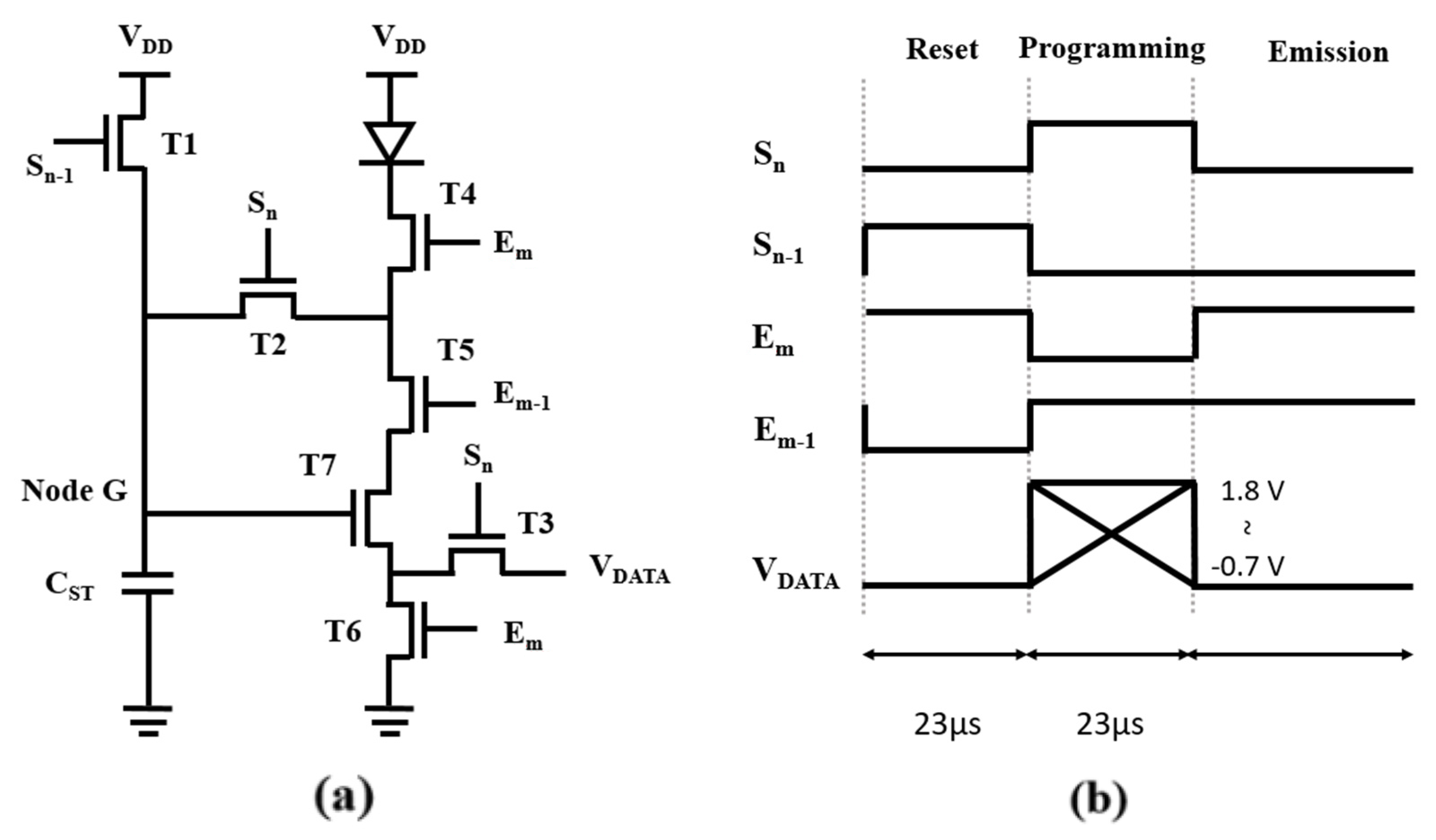
2. Proposed Pixel Circuit Operation
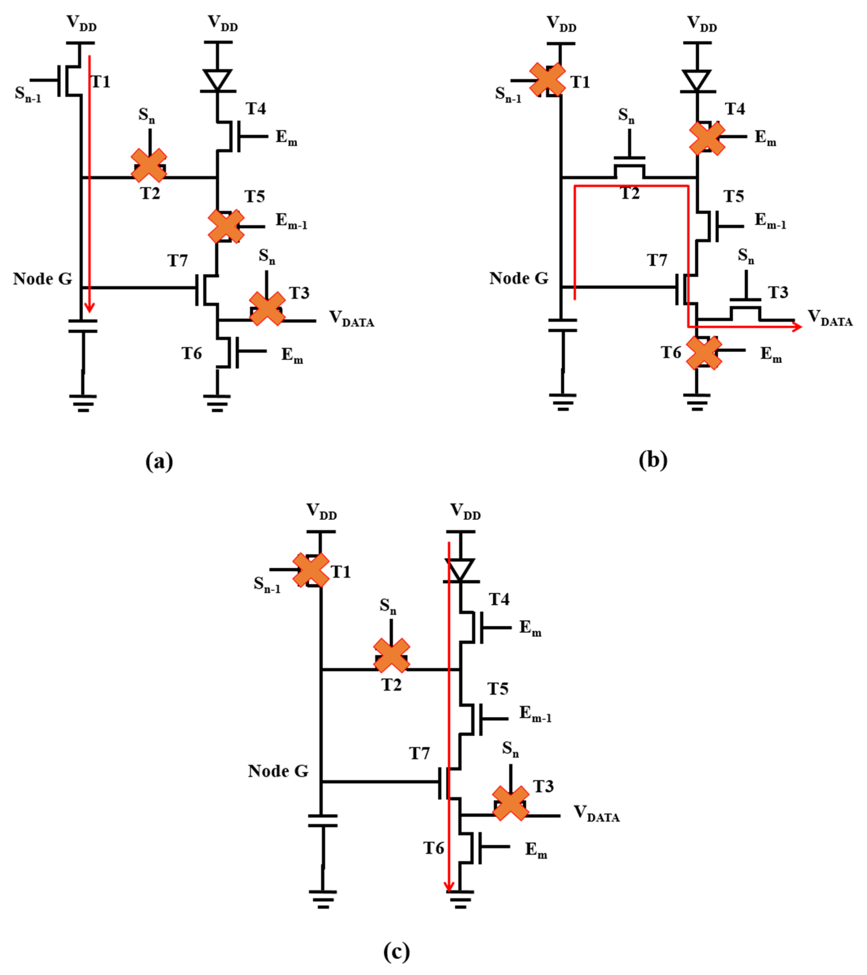
2.1. Reset
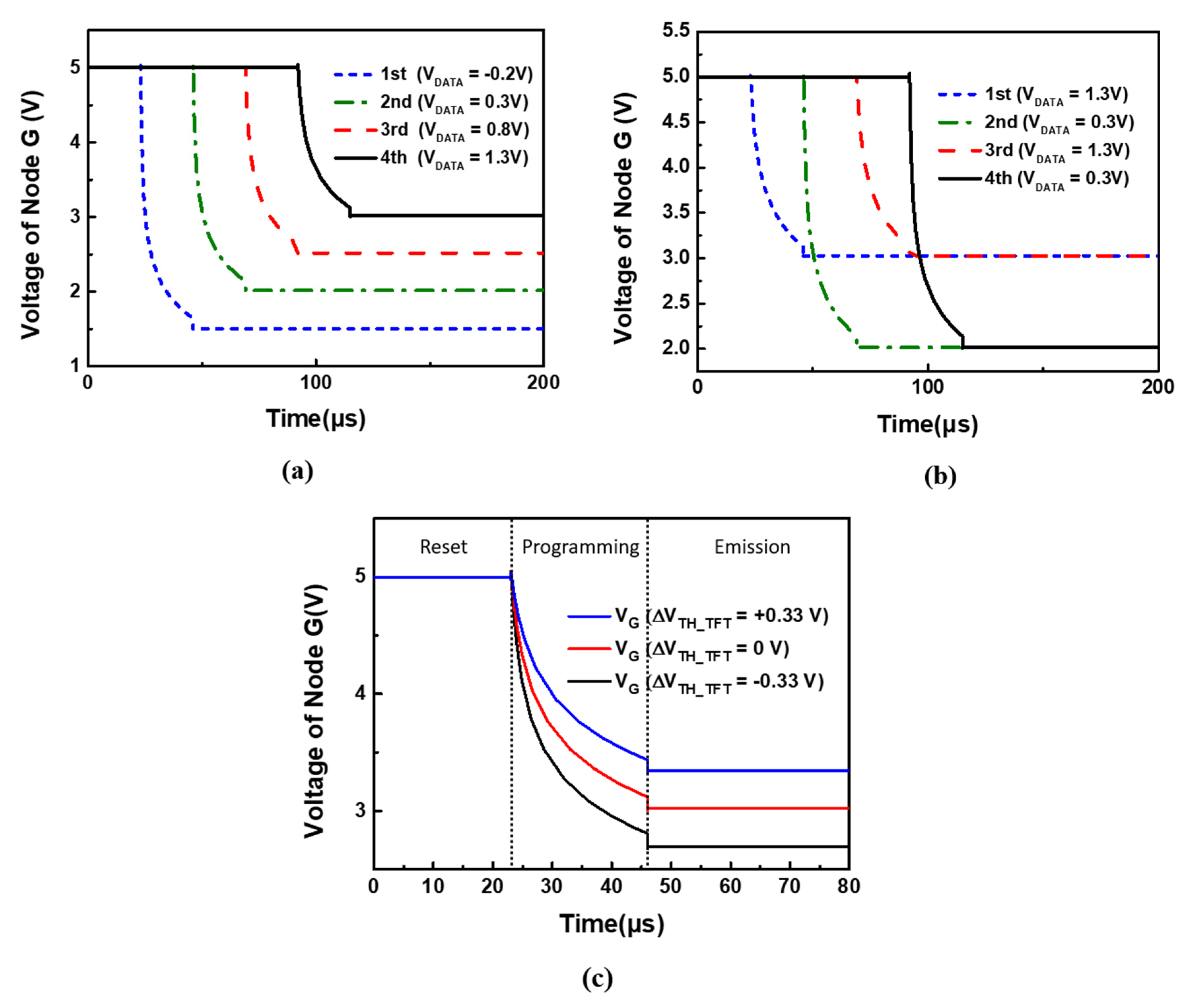
2.2. Programming
2.3. Emission
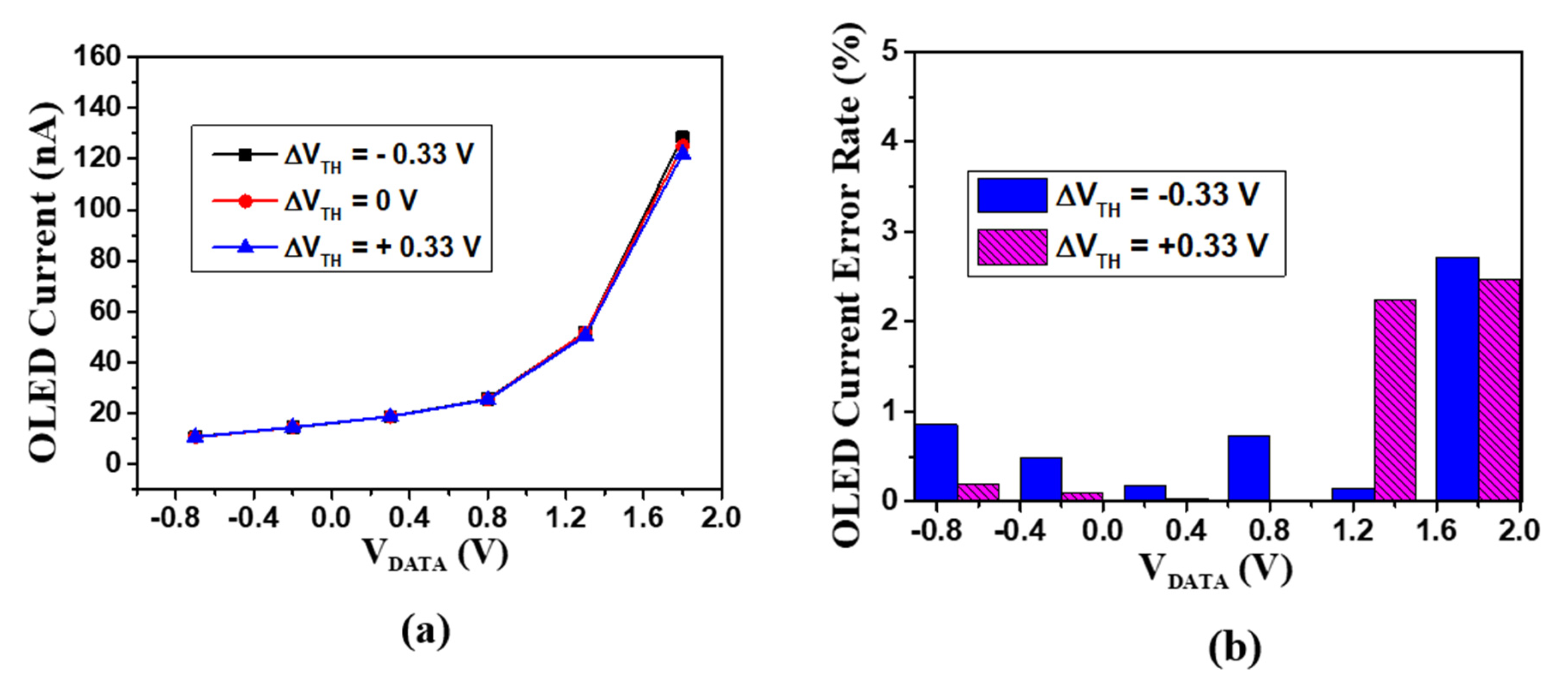
3. Results and Discussion
4. Conclusions
Author Contributions
Funding
Acknowledgments
Conflicts of Interest
References
- Dawson, R.; Shen, Z.; Furst, D.; Connor, S.; Hsu, J.; Kane, M.; Stewart, R.; Ipri, A.; King, C.; Green, P.; et al. The impact of the transient response of organic light emitting diodes on the design of active matrix OLED displays. In International Electron Devices Meeting 1998. Technical Digest (Cat. No.98CH36217); IEEE: Piscataway, NJ, USA, 2002; pp. 875–878. [Google Scholar]
- Wang, C.; Hu, Z.; He, X.; Liao, C.; Zhang, S. One Gate Diode-Connected Dual-Gate a-IGZO TFT Driven Pixel Circuit for Active Matrix Organic Light-Emitting Diode Displays. IEEE Trans. Electron Devices 2016, 63, 3800–3803. [Google Scholar] [CrossRef]
- Chen, H.-W.; Lee, J.-H.; Lin, B.-Y.; Chen, S.; Wu, S.-T. Liquid crystal display and organic light-emitting diode display: Present status and future perspectives. Light. Sci. Appl. 2018, 7, 17168. [Google Scholar] [CrossRef] [PubMed]
- Huang, Y.; Hsiang, E.-L.; Deng, M.-Y.; Wu, S.-T. Mini-LED, Micro-LED and OLED displays: Present status and future perspectives. Light. Sci. Appl. 2020, 9, 105. [Google Scholar] [CrossRef] [PubMed]
- Fan, C.-L.; Tseng, F.-P.; Lai, H.-L.; Sun, B.-J.; Chao, K.-C.; Chen, Y.-C. A Novel LTPS-TFT Pixel Circuit to Compensate the Electronic Degradation for Active-Matrix Organic Light-Emitting Diode Displays. Int. J. Photoenergy 2013, 2013, 839301. [Google Scholar] [CrossRef] [Green Version]
- Lin, C.-L.; Chen, Y.-C. A Novel LTPS-TFT Pixel Circuit Compensating for TFT Threshold-Voltage Shift and OLED Degradation for AMOLED. IEEE Electron Device Lett. 2007, 28, 129–131. [Google Scholar] [CrossRef]
- Lu, H.-Y.; Chang, T.-C.; Tai, Y.-H.; Liu, P.-T.; Chi, S. A New Pixel Circuit Compensating for Brightness Variation in Large Size and High Resolution AMOLED Displays. J. Disp. Technol. 2007, 3, 398–403. [Google Scholar] [CrossRef]
- Lin, C.-L.; Hsu, C.-C.; Chen, P.-S.; Lai, P.-C.; Lee, P.-T.; Kuo, P.-Y. Suppressing Vth Variations in LTPS Thin-Film Transistors with Current Scaling Ratio Modulation for AMOLED Display. IEEE Trans. Electron Devices 2018, 65, 3577–3581. [Google Scholar] [CrossRef]
- Nathan, A.; Chaji, G.; Ashtiani, S.J. Driving Schemes for a-Si and LTPS AMOLED Displays. J. Disp. Technol. 2005, 1, 267–277. [Google Scholar] [CrossRef]
- Ma, P.; Sun, J.; Zhang, G.; Liang, G.; Xin, Q.; Li, Y.; Song, A. Low–temperature fabrication of HfAlO alloy dielectric using atomic–layer deposition and its application in a low–power device. J. Alloys Compd. 2019, 792, 543–549. [Google Scholar] [CrossRef]
- Lin, C.L.; Chen, F.H.; Hung, C.C.; Chen, P.S.; Deng, M.Y.; Lu, C.M.; Huang, T.H. New a-IGZO Pixel Circuit Composed of Three Transistors and One Capacitor for Use in High-Speed-Scan AMOLED Displays. J. Disp. Technol. 2015, 11, 1031–1034. [Google Scholar] [CrossRef]
- Watakabe, H.; Jinnai, T.; Suzumura, I.; Hanada, A.; Onodera, R.; Tada, M.; Mochizuki, K.; Tanaka, H.; Ito, T. 39-2: Development of Advanced LTPS TFT Technology for Low Power Consumption and Narrow Border LCDs. SID Symp. Dig. Tech. Pap. 2019, 50, 541–544. [Google Scholar] [CrossRef]
- Chung, H.-J. Novel 5T1C pixel circuit for high-ppi AMOLED displays with n-channel LTPS TFTs. J. Inf. Disp. 2019, 20, 39–43. [Google Scholar] [CrossRef] [Green Version]
- Chang, T.-K.; Lin, C.-W.; Chang, S. 39-3: Invited Paper: LTPO TFT Technology for AMOLEDs. SID Symp. Dig. Tech. Pap. 2019, 50, 545–548. [Google Scholar] [CrossRef]
- Lin, C.-L.; Chang, J.-H.; Lai, P.-C.; Shih, L.-W.; Chen, S.-C.; Cheng, M.-H. Pixel Circuit with Leakage Prevention Scheme for Low-Frame-Rate AMOLED Displays. IEEE J. Electron Devices Soc. 2020, 8, 235–240. [Google Scholar] [CrossRef]
- Fan, C.-L.; Chen, Y.-C.; Yang, C.-C.; Tsai, Y.-K.; Huang, B.-R. Novel LTPS-TFT Pixel Circuit with OLED Luminance Compensation for 3D AMOLED Displays. J. Disp. Technol. 2016, 12, 425–428. [Google Scholar] [CrossRef]
- Lin, C.-L.; Chen, P.-S.; Lai, P.-C.; Chu, T.-C.; Wang, M.-X.; Lee, C.-L. Novel Pixel Circuit with Compensation for Normally-Off/On a-IGZO TFTs and OLED Luminance Degradation. J. Disp. Technol. 2016, 12, 1. [Google Scholar] [CrossRef]
- Liu, P.-T.; Chu, L.-W.; Teng, L.-F.; Fan, Y.-S.; Fuh, C.-S. Transparent Amorphous Oxide Semiconductors for System on Panel Applications. ECS Meet. Abstr. 2012, 50, 257–268. [Google Scholar] [CrossRef]
- Sze, S.M.; Ng, K.K. Physics of Semiconductor Devices; Wiley Interscience: Hoboken, NJ, USA, 2007. [Google Scholar]


| Ref | This Study | [13] | [14] | [15] | [16] |
|---|---|---|---|---|---|
| Signal lines | 2 | 2 | 4 | 3 | 4 |
| V TH_DTFTvariation error rate | 2.71% (ΔVTH = ±0.33 V) | 14.11% (ΔVTH = ±0.5 V) | Null | 4.73% (ΔVTH = ±0.5 V) | 2.8% (ΔVTH = ±0.33 V) |
| Driving voltage (VDD & VSS) | VDD = 5 V VSS = 0 V | VDD = 11 V VSS = 0 V | Null | VDD = 3.3 V VSS = −3.3 V | VDD = 12 V VSS = 0 V |
| Backplane technology | LTPO | LTPS | LTPO | LTPS | LTPS |
| Minimum frame rate | 1 Hz | 60 Hz | 1 Hz | 15 Hz | 240 Hz |
Publisher’s Note: MDPI stays neutral with regard to jurisdictional claims in published maps and institutional affiliations. |
© 2021 by the authors. Licensee MDPI, Basel, Switzerland. This article is an open access article distributed under the terms and conditions of the Creative Commons Attribution (CC BY) license (https://creativecommons.org/licenses/by/4.0/).
Share and Cite
Fan, C.-L.; Lin, W.-Y.; Chen, C.-Y. New Low-Frame-Rate Compensating Pixel Circuit Based on Low-Temperature Poly-Si and Oxide TFTs for High-Pixel-Density Portable AMOLED Displays. Micromachines 2021, 12, 1514. https://doi.org/10.3390/mi12121514
Fan C-L, Lin W-Y, Chen C-Y. New Low-Frame-Rate Compensating Pixel Circuit Based on Low-Temperature Poly-Si and Oxide TFTs for High-Pixel-Density Portable AMOLED Displays. Micromachines. 2021; 12(12):1514. https://doi.org/10.3390/mi12121514
Chicago/Turabian StyleFan, Ching-Lin, Wei-Yu Lin, and Chun-Yuan Chen. 2021. "New Low-Frame-Rate Compensating Pixel Circuit Based on Low-Temperature Poly-Si and Oxide TFTs for High-Pixel-Density Portable AMOLED Displays" Micromachines 12, no. 12: 1514. https://doi.org/10.3390/mi12121514
APA StyleFan, C.-L., Lin, W.-Y., & Chen, C.-Y. (2021). New Low-Frame-Rate Compensating Pixel Circuit Based on Low-Temperature Poly-Si and Oxide TFTs for High-Pixel-Density Portable AMOLED Displays. Micromachines, 12(12), 1514. https://doi.org/10.3390/mi12121514