
Radiation Hardness Property of Ultra-Fast 3D-Trench Electrode Silicon Detector on N-Type Substrate


Abstract
:1. Introduction
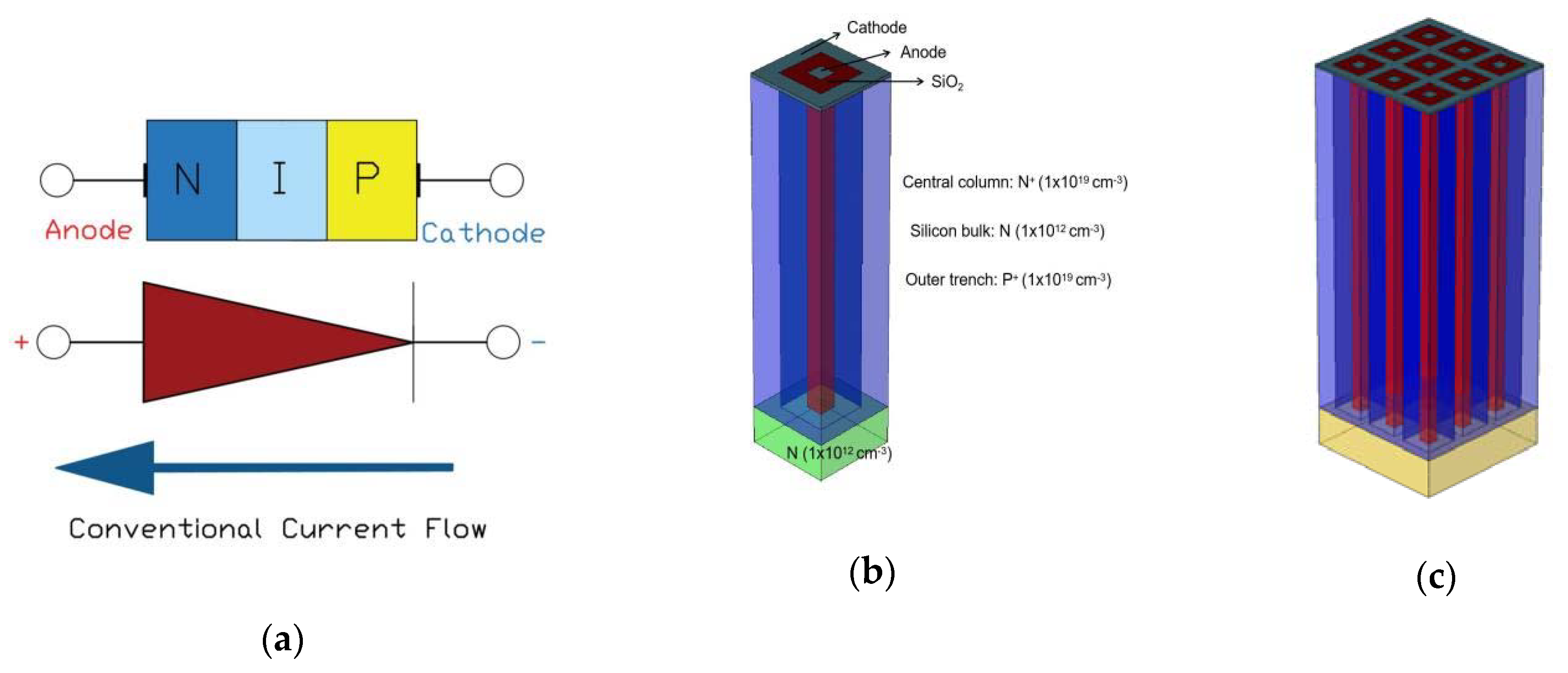
2. Device Modeling
3. Electrical Characteristics of the Ultra-Fast 3D-Trench Electrode Detector with Variety Radiation Fluences
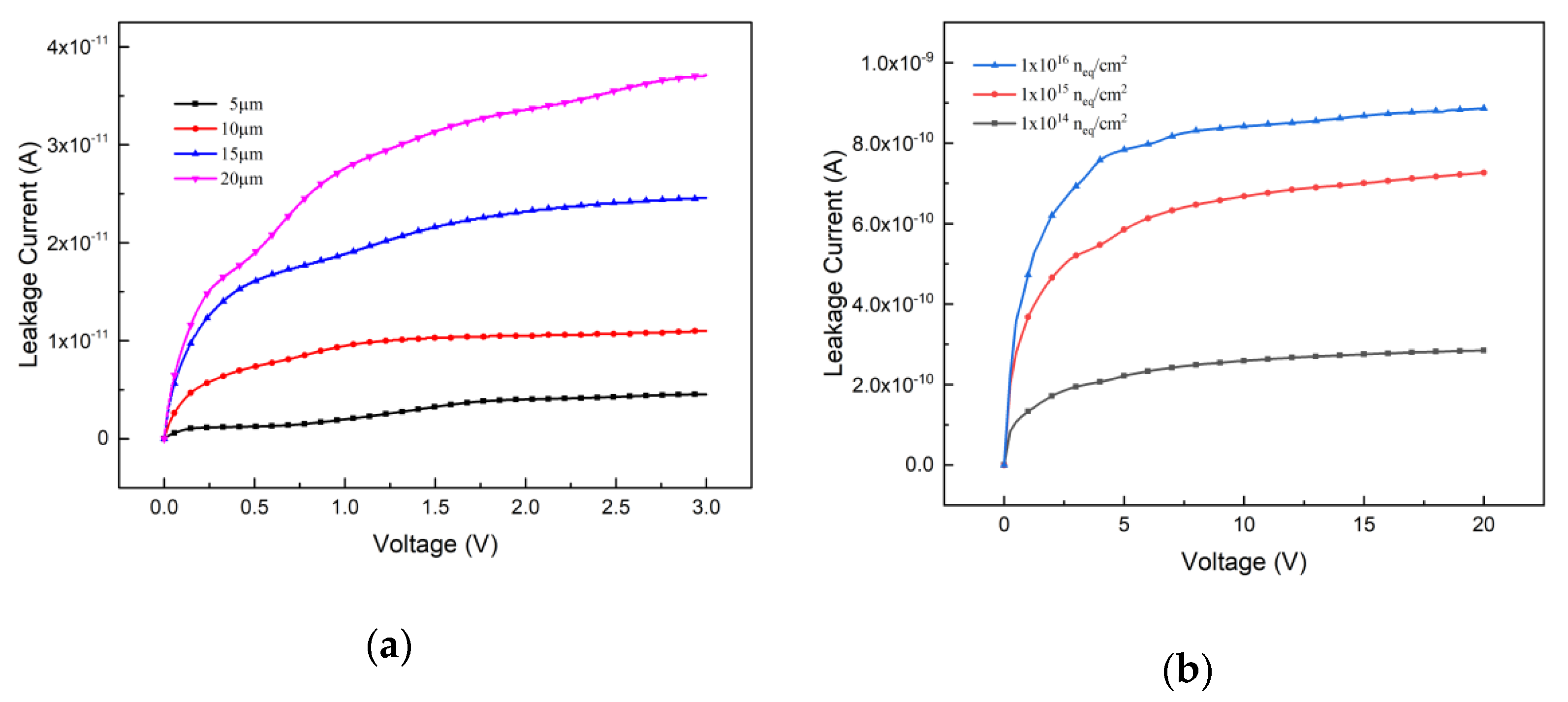
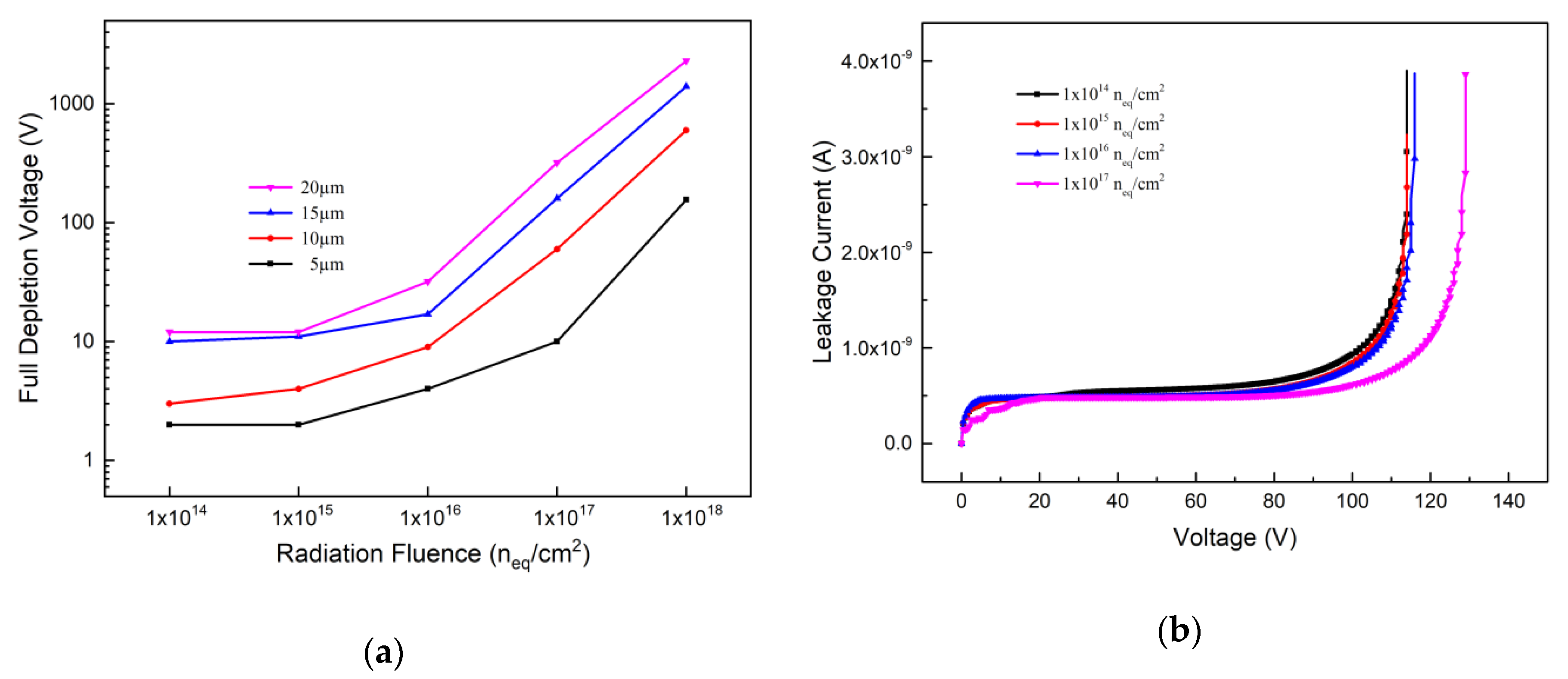
3.1. Leakage Current
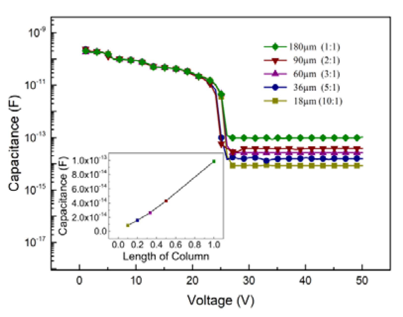
3.2. Capacitance
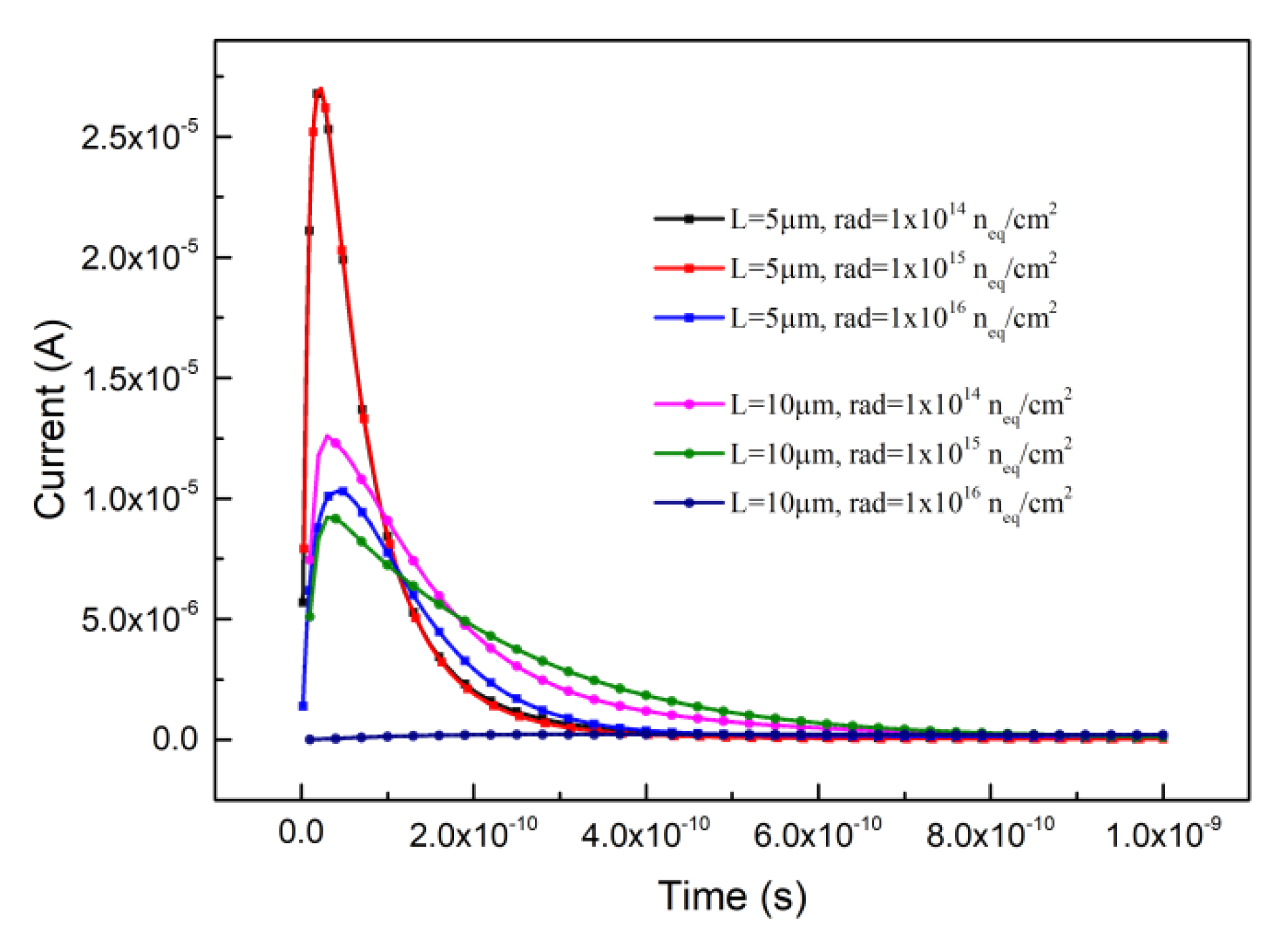
3.3. The Transient Induced Current
3.4. Full Depletion Voltage and Breakdown Voltage
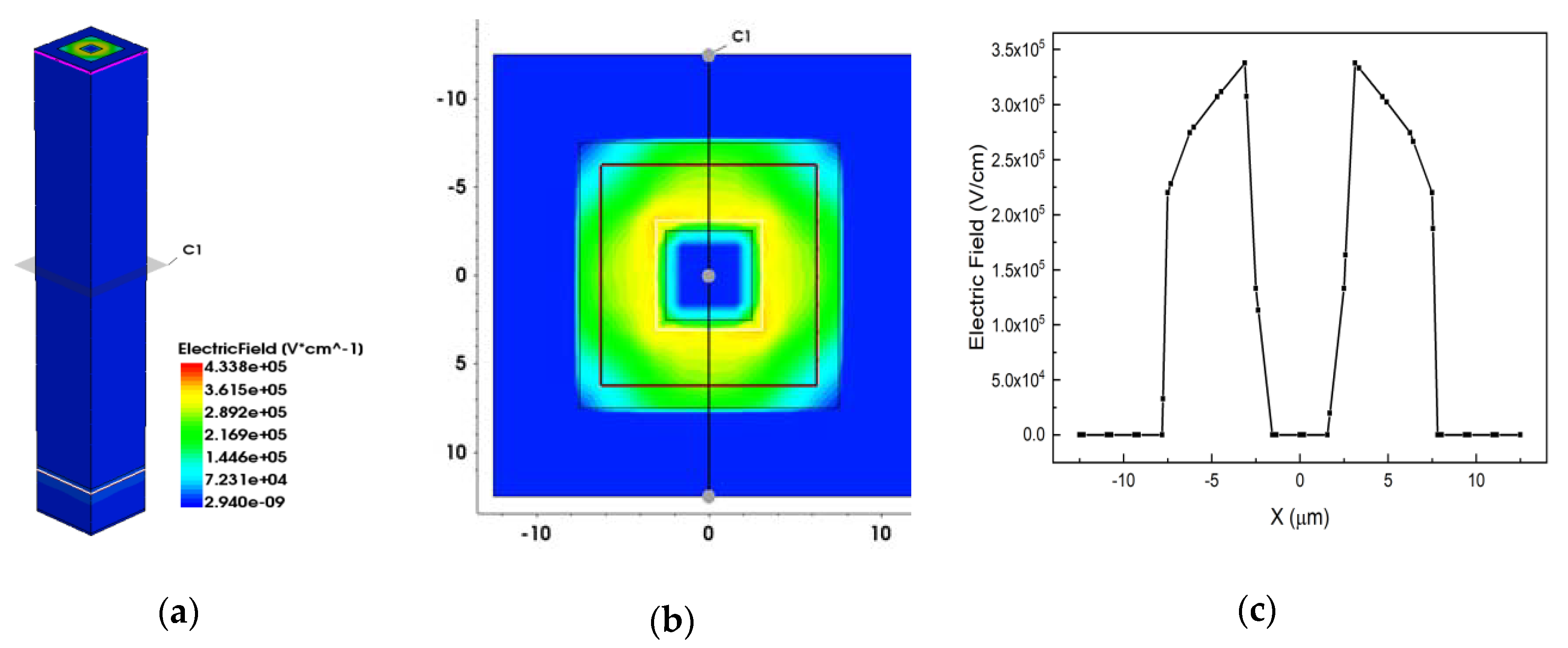
3.5. The Weighting Field
4. Conclusions
Author Contributions
Funding
Conflicts of Interest
References
- Parker, S.; Kenney, C.; Segal, J. 3D—A proposed new architecture for solid-state radiation detectors. Nucl. Instrum. Methods Phys. Res. Sect. A Accel. Spectrom. Detect. Assoc. Equip. 1997, 395, 328–343. [Google Scholar] [CrossRef]
- Kenney, C.; Parker, S.; Segal, J.; Storment, C. Silicon detectors with 3-D electrode arrays: Fabrication and initial test results. IEEE Trans. Nucl. Sci. 1999, 46, 1224–1236. [Google Scholar] [CrossRef] [Green Version]
- DaVia, C.; Hasia, J.; Kenney, C.; Koka, A.; Parker, S. 3D silicon detectors—Status and applications. Nucl. Instrum. Methods Phys. Res. Sect. A Accel. Spectrom. Detect. Assoc. Equip. 2005, 549, 122–125. [Google Scholar] [CrossRef]
- Li, Z. New BNL 3D-Trench electrode Si detectors for radiation hard detectors for sLHC and for X-ray applications. Nucl. Instrum. Methods Phys. Res. Sect. A Accel. Spectrom. Detect. Assoc. Equip. 2011, 658, 90–97. [Google Scholar] [CrossRef]
- Parker, S.; Kok, A.; Kenney, C.; Jarron, P.; Hasi, J.; Despeisse, M.; Da Via, C.; Anelli, G. Increased speed: 3D silicon sensors. Fast current amplifiers. IEEE Trans. Nucl. Sci. 2011, 58, 404–417. [Google Scholar] [CrossRef] [Green Version]
- Piemonte, C.; Boscardin, M.; Betta, G.F.D.; Ronchin, S.; Zorzi, N. Development of 3D detectors featuring columnar electrodes of the same doping type. Nucl. Instrum. Methods Phys. Res. Sect. A Accel. Spectrom. Detect. Assoc. Equip. 2005, 541, 441–448. [Google Scholar] [CrossRef]
- Li, Z.; Chen, W.; Guo, Y.; Lissauer, D.; Lynn, D.; Radeka, V.; Pellegrini, G. Development, simulation and processing of new 3D Si detectors. Nucl. Instrum. Methods Phys. Res. Sect. A Accel. Spectrom. Detect. Assoc. Equip. 2007, 583, 139–148. [Google Scholar] [CrossRef]
- Grönlund, T.; Li, Z.; Carini, G.; Li, M. Full 3D simulations of BNL one-sided silicon 3D detectors and comparisons with other types of 3D detectors. Nucl. Instrum. Methods Phys. Res. Sect. A Accel. Spectrom. Detect. Assoc. Equip. 2008, 586, 180–189. [Google Scholar] [CrossRef]
- Kok, A.; Hansen, T.E.; Hansen, T.A.; Lietaer, N. Fabrication of 3D Silicon Sensors. In Proceedings of the 19th International Workshop on Vertex Detectors—VERTEX 2010, Loch Lomond, Scotland, 6–11 June 2010. [Google Scholar]
- Betta, G.-F.D.; Boscardin, M.; Bosisio, L.; Piemonte, C.; Ronchin, S.; Zoboli, A.; Zorzi, N. New developments on 3D detectors at IRST. 2007 IEEE Nucl. Sci. Symp. Conf. Rec. 2007, 2, 983–987. [Google Scholar] [CrossRef]
- Zoboli, A.; Boscardin, M.; Bosisio, L.; Betta, G.-F.D.; Piemonte, C.; Ronchin, S.; Zorzi, N. Double-Sided, Double-Type-Column 3-D Detectors: Design, Fabrication, and Technology Evaluation. IEEE Trans. Nucl. Sci. 2008, 55, 2775–2784. [Google Scholar] [CrossRef]
- Pellegrini, G.; Lozano, M.; Ullan, M.; Bates, R.; Fleta, C.; Pennicard, D. Pennicard. First double-sided 3-D detectors fabricated at CNM-IMB. Nucl. Instrum. Methods Phys. Res. Sect. A Accel. Spectrom. Detect. Assoc. Equip. 2008, 592, 38–43. [Google Scholar] [CrossRef]
- Betta, G.-F.D.; Bagolini, A.; Boscardin, M.; Bosisio, L.; Gabos, P.; Giacomini, G.; Piemonte, C.; Povoli, M.; Vianello, E.; Zorzi, N. Development of modified 3D detectors at FBK. In Proceedings of the IEEE Nuclear Science Symposium, Knoxville, TN, USA, 30 October–6 November 2010; p. N15-3. [Google Scholar]
- Pellegrini, G.; Balbuena, J.P.; Bassignana, D.; Cabruja, E.; Fleta, C.; Guardiola, C.; Lozano, M.; Quirion, D.; Ullán, M. 3D double sided detector fabrication at IMB-CNM. Nucl. Instrum. Methods Phys. Res. Sect. A Accel. Spectrom. Detect. Assoc. Equip. 2012, 699, 27–30. [Google Scholar] [CrossRef]
- Duarte-Campderros, J.; Curras, E.; Fernandez, M.; Gomez, G.; Garcia, A.; Gonzalez, J.; Silva, E.; Vila, I.; Jaramillo, R.; Meschini, M.; et al. Results on proton-irradiated 3D pixel sensors interconnected to RD53A readout ASIC. Nucl. Instrum. Methods Phys. Res. Sect. A Accel. Spectrom. Detect. Assoc. Equip. 2019, 944, 16–25. [Google Scholar] [CrossRef] [Green Version]
- Kramberger, G.; Cindro, V.; Flores, D.; Hidalgo, S.; Hiti, B.; Manna, M.; Mandić, I.; Mikuž, M.; Quirion, D.; Pellegrini, G.; et al. Timing performance of small cell 3D silicon detectors. Nucl. Instrum. Methods Phys. Res. Sect. A Accel. Spectrom. Detect. Assoc. Equip. 2019, 934, 26–32. [Google Scholar] [CrossRef] [Green Version]
- Ellakany, A.; Shaker, A.; Abouelatta, M.; Hafez, I.M.; Gontrand, C. Modeling and simulation of a hybrid 3D silicon detector system using SILVACO and Simulink/MATLAB framework. In Proceedings of the 2016 28th International Conference on Microelectronics (ICM), Giza, Egypt, 17–20 December 2016; pp. 377–380. [Google Scholar]
- Bergmann, B.; Pichotka, M.; Pospisil, S.; Vycpalek, J.; Burian, P.; Broulim, P.; Jakubek, J. 3D track reconstruction capability of a silicon hybrid active pixel detector. Eur. Phys. J. C 2017, 77, 421. [Google Scholar] [CrossRef] [Green Version]
- Hansen, T.-E.; Kok, A.; Hansen, T.A.; Lietaer, N.; Mielnik, M.; Storås, P.; Da Via, C.; Hasi, J.; Kenney, C.; Parker, S. First fabrication of full 3D-detectors at SINTEF. J. Instrum. 2009, 4, P03010. [Google Scholar] [CrossRef]
- Da Via, C.; Hasi, J.; Kenney, C.; Linhart, V.; Parker, S.; Slavicek, T.; Watts, S.J.; Bem, P.; Horazdovsky, T.; Pospisil, S. Radiation hardness properties of full-3D active edge silicon sensors. Nucl. Instrum. Methods Phys. Res. Sect. A Accel. Spectrom. Detect. Assoc. Equip. 2008, 587, 243–249. [Google Scholar] [CrossRef]
- Boscardin, M.; Ferrari, S.; Ficorella, F.; Lai, A.; Mendicino, R.; Meschini, M.; Ronchin, S.; Samy, M.A.A.; Dalla Betta, G.F. Advances in 3D Sensor Technology by Using Stepper Lithography. Front. Phys. 2021, 8, 625275. [Google Scholar] [CrossRef]
- Terzo, S.; Grinstein, S.; Manna, M.; Pellegrini, G.; Quirion, D. A new generation of radiation hard 3D pixel sensors for the ATLAS upgrade. Nucl. Instrum. Methods Phys. Res. Sect. A Accel. Spectrom. Detect. Assoc. Equip. 2020, 982, 164587. [Google Scholar] [CrossRef]
- Manna, M.; Grieco, C.; Grinstein, S.; Hidalgo, S.; Pellegrini, G.; Quirion, D.; Terzo, S. First characterisation of 3D pixel detectors irradiated at extreme fluences. Nucl. Instrum. Methods Phys. Res. Sect. A Accel. Spectrom. Detect. Assoc. Equip. 2020, 979, 164458. [Google Scholar] [CrossRef]
- Gianotti, F.; Mangano, M.L.; Virdee, T.; Abdullin, S.; Azuelos, G.; Ball, A.H.; Barberis, D.; Belyaev, A.; Bloch, P.; Bosman, M.; et al. Physics potential and experimental challenges of the LHC luminosity upgrade. Eur. Phys. J. C 2005, 39, 293–333. [Google Scholar] [CrossRef]
- Baselga, M.; Pellegrini, G.; Quirion, D. Simulations of 3D-Si sensors for the innermost layer of the ATLAS pixel upgrade. Nucl. Instrum. Methods Phys. Res. Sect. A Accel. Spectrom. Detect. Assoc. Equip. 2017, 847, 67–76. [Google Scholar] [CrossRef] [Green Version]
- Li, Z.; Abreu, M.C.; Anbinderis, P.; D’Ambrosio, N.; De Boer, W.; Borchi, E.; Borer, K.; Bruzzi, M.; Buontempo, S.; Chen, W.; et al. Development of cryogenic Si detectors by CERN RD39 Collaboration for ultra radiation hardness in SLHC environment. Nucl. Instrum. Methods Phys. Res. Sect. A Accel. Spectrom. Detect. Assoc. Equip. 2006, 572, 305–310. [Google Scholar] [CrossRef]
- Montalbano, A.; Bassignana, D.; Li, Z.; Liu, S.; Lynn, D.; Pellegrini, G.; Tsybychev, D. A systematic study of BNL’s 3D-Trench Electrode detectors. Nucl. Instrum. Methods Phys. Res. Sect. A Accel. Spectrom. Detect. Assoc. Equip. 2014, 765, 23–28. [Google Scholar] [CrossRef]
- Ding, H.; Chen, J.; Li, Z.; Yan, S. Modeling and simulation of charge collection properties for 3D-trench electrode detector. Nucl. Instrum. Methods Phys. Res. Sect. A Accel. Spectrom. Detect. Assoc. Equip. 2015, 796, 29–33. [Google Scholar] [CrossRef]
- Chen, J.; Ding, H.; Li, Z.; Yan, S. 3D simulations of device performance for 3D-Trench electrode detector. Nucl. Instrum. Methods Phys. Res. Sect. A Accel. Spectrom. Detect. Assoc. Equip. 2015, 796, 34–37. [Google Scholar] [CrossRef]
- Liu, M.; Li, Z.; Feng, M. 3D Simulation and Modeling of Ultra-fast 3D Silicon Detectors. MATEC Web Conf. 2017, 108, 09006. [Google Scholar] [CrossRef]
- Liu, M.-W.; Li, Z. Development of Ultra-fast 3D Silicon Detectors: 3D Simulation and Modeling of 3D-trench Electrode Detector. In Proceedings of the Advances in Engineering Research, 3rd Annual International Conference on Advanced Material Engineering, Shanghai, China, 14–16 April 2017; Volume 110. [Google Scholar]
- Liu, M.; Zhou, T.; Li, Z. Electrical Properties of Ultra-Fast 3D-Trench Electrode Silicon Detector. Micromachines 2020, 11, 674. [Google Scholar] [CrossRef]
- Morozzi, A.; Moscatelli, F.; Croci, T.; Passeri, D. TCAD Modeling of Surface Radiation Damage Effects: A State-Of-The-Art Review. Front. Phys. 2021, 9, 617322. [Google Scholar] [CrossRef]
- Moscatelli, F.; Passeri, D.; Morozzi, A.; Mendicino, R.; Dalla Betta, G.F.; Bilei, G.M. Combined Bulk and Surface Radia-tion Damage Effects at Very High Fluences in Silicon Detectors: Measurements and TCAD Simulations. IEEE Trans. Nucl. Sci. 2016, 63, 5. [Google Scholar] [CrossRef] [Green Version]
- Schwandt, J.; Fretwurst, E.; Garutti, E.; Klanner, R.; Scharf, C.; Steinbrueck, G. A new model for the TCAD simulation of the silicon damage by high fluence proton irradiation. In Proceedings of the 2018 IEEE Nuclear Science Symposium and Medical Imaging Conference (NSS/MIC), Sydney, Australia, 10–17 November 2018. [Google Scholar] [CrossRef]
- Folkestad, Å.; Akiba, K.; Van Beuzekom, M.; Buchanan, E.; Collins, P.; Dall’Occo, E.; Di Canto, A.; Evans, T.; Lima, V.F.; Pardiñas, J.G.; et al. Development of a silicon bulk radiation damage model for Sentaurus TCAD. Nucl. Instrum. Methods Phys. Res. Sect. A Accel. Spectrom. Detect. Assoc. Equip. 2017, 874, 94–102. [Google Scholar] [CrossRef]
- Li, Z. Radiation damage effects in Si materials and detectors and rad-hard Si detectors for SLHC. J. Instrum. 2009, 4, P03011. [Google Scholar] [CrossRef]
- Schroder, D.K. Semiconductor Material and Device Characterization, 3rd ed.; John Wiley & Sons: Hoboken, NJ, USA, 2005. [Google Scholar] [CrossRef]
- Kraner, H.W.; Li, Z.; Posnecker, K.U. Fast neutron damage in silicon detectors. Nucl. Instrum. Methods Phys. Res. Sect. A Accel. Spectrom. Detect. Assoc. Equip. 1989, 279, 266–271. [Google Scholar] [CrossRef] [Green Version]
- Hoedlmoser, H.; Moll, M.; Härkönen, J.; Kronberger, M.; Trummer, J.; Rodeghiero, P. Characterization of 150 μm thick epi-taxial silicon detectors from different producers after proton irradiation. Nucl. Instrum. Methods Phys. Res. Sect. A Accel. Spectrom. Detect. Assoc. Equip. 2007, 580, 1243–1249. [Google Scholar] [CrossRef]
- Li, Z.; Kraner, H.W. Modeling and simulation of charge collection properties for neutron irradiated silicon detectors. Nucl. Phys. B Proc. Suppl. 1993, 32, 398–409. [Google Scholar] [CrossRef]
- Bruzzi, M.; Adey, J.; Al-Ajili, A.; Alexandrov, P.; Alfieri, G.; Allport, P.P.; Andreazza, A.; Artuso, M.; Assouak, S.; Avset, B.S.; et al. Radiation-hard semiconductor detectors for SuperLHC. Nucl. Instrum. Methods Phys. Res. Sect. A Accel. Spectrom. Detect. Assoc. Equip. 2005, 541, 189–201. [Google Scholar] [CrossRef]

Publisher’s Note: MDPI stays neutral with regard to jurisdictional claims in published maps and institutional affiliations. |
© 2021 by the authors. Licensee MDPI, Basel, Switzerland. This article is an open access article distributed under the terms and conditions of the Creative Commons Attribution (CC BY) license (https://creativecommons.org/licenses/by/4.0/).
Share and Cite
Liu, M.; Li, X.; Cheng, W.; Li, Z.; Li, Z. Radiation Hardness Property of Ultra-Fast 3D-Trench Electrode Silicon Detector on N-Type Substrate. Micromachines 2021, 12, 1400. https://doi.org/10.3390/mi12111400
Liu M, Li X, Cheng W, Li Z, Li Z. Radiation Hardness Property of Ultra-Fast 3D-Trench Electrode Silicon Detector on N-Type Substrate. Micromachines. 2021; 12(11):1400. https://doi.org/10.3390/mi12111400
Chicago/Turabian StyleLiu, Manwen, Xinqing Li, Wenzheng Cheng, Zheng Li, and Zhihua Li. 2021. "Radiation Hardness Property of Ultra-Fast 3D-Trench Electrode Silicon Detector on N-Type Substrate" Micromachines 12, no. 11: 1400. https://doi.org/10.3390/mi12111400
APA StyleLiu, M., Li, X., Cheng, W., Li, Z., & Li, Z. (2021). Radiation Hardness Property of Ultra-Fast 3D-Trench Electrode Silicon Detector on N-Type Substrate. Micromachines, 12(11), 1400. https://doi.org/10.3390/mi12111400