Abstract
In this paper, a memristor model based on FPGA (field programmable gate array) is proposed, by using which the circuit of AND gate and OR gate composed of memristors is built. Combined with the original NOT gate in FPGA, the NAND gate, NOR gate, XOR gate and the XNOR gate are further realized, and then the adder design is completed. Compared with the traditional gate circuit, this model has distinct advantages in size and non-volatility. At the same time, the establishment of this model will add new research methods and tools for memristor simulation research.
1. Introduction
In 1971, Professor Chua proposed the fourth passive basic device memristor [1], which is directly used to characterize the relationship between charge and magnetic flux. In 2008, the HP laboratory published the paper “The missing memristor found” in Nature and announced the successful implementation of the world’s first memristor physical device [2]. It was found that memristor can perform Boolean logic operations and can completely replace the existing digital logic circuit in theory. In addition, the memristor has a wide application prospect in storage devices, logic circuits, analog circuits and so on.
According to the characteristics of the HP memristor with small ON resistance and large OFF resistance [3], the high and low binary resistance characteristics of the memristor can be applied to digital logic circuits [4,5]. Because the digital logic circuit based on the memristor has a smaller area and lower power consumption, it has been widely studied by researchers in recent years, such as memristor-based material implication (IMPLY) logic circuits, memristor aided logic (MAGIC) circuits and memristor ratio logic (MRL) circuits, etc. In 2010, the HP laboratory first mentioned that the simple circuit composed of memristor and resistor can realize material implementation logic operation (IMP), and then combine FALSE operation to form a logic unit, which can realize the operation of arbitrary Boolean logic function [6]. Then, other circuits based on the memristor by IMP were designed, such as the CMOS-memristor circuit, which can reduce the length of the calculation sequence, or use fewer execution steps and a smaller number of memristors [7,8,9]. Considering the complexity of IMP logic based on the memristor, the MAGIC circuit is proposed, which was simpler and more stable. Subsequently, many improved circuits based on the MAGIC circuit were proposed. By evaluating circuit performance in different ways, it is found that this kind of memristor based circuits with the advantages of reducing circuit area and increasing computing speed [10,11,12,13,14,15]. At the same time, a lot of research has been focused on the MRL circuits composed of memristors and CMOS transistors based on the compatibility of memristor and CMOS transistors. This kind of circuit has fewer devices, less circuit area and power consumption, and also the data density is improved. [16,17,18,19]. In recent years, many digital logic circuits based on memristors and CMOS transistors have been proposed, such as adders [20,21], multipliers [22,23,24], counters [25], decoders [26] and maximum and minimum circuits [14], etc., which play an important role in digital systems.
Therefore, although the fourth kind of basic circuit components, memristor has a great application prospect and research space in the digital logic circuit, all of these memristor based circuits mentioned above focus on circuits design and performance assessment only. Considering the field programmable gate array (FPGA) is a programmable logic array, and it is a good choice to apply memristors to digital circuits, the memristor is modeled in FPGA in this paper. On the one hand, FPGA as a semi-custom circuit in the field of ASIC, not only solves the shortage of custom circuit, but also overcomes the disadvantage of the limited number of original programmable gate circuits. It can program almost infinitely and greatly reduce the cost. On the other hand, a memristor can be applied to digital circuits, and FPGA is a programmable logic array where analog memristor can be directly combined or compared with other gate circuits, without connecting or borrowing other platforms, which reduces the complexity of the transition and comparison steps in the research process and can greatly improve the research efficiency. On this basis, combined with the ON and OFF characteristics of a memristor, the AND gate and OR gate t based on FPGA are realized by the memristor, and the design of the memristor adder is realized too.
The structure of this paper is as follows: firstly, the working principle of the HP memristor is introduced and the circuit model of the threshold memristor is established in FPGA based on this principle; secondly, on the basis of the established model, FPGA AND gate and OR gate circuits based on the memristor are realized. Thirdly, the memristor CMOS and NOR gate, NOR gate, XOR gate and XNOR gate are realized by combining with the NOT gate circuit in FPGA. Finally, the adder is designed by using the logic gates. Compared with traditional CMOS circuits, the memristor-based logic circuit can not only increase the density of the device, but also reduce the power consumption and improve the operation speed of the circuit.
2. Working Principle and Threshold Characteristic Analysis of HP Memristor
In 1971, Professor Chua defined the memristor according to the functional relationship between φ and q: dφ = M(q)dq, where dφ = Vdt, dq = Idt. M is a variable with the same physical dimension as the resistance, and its value depends on the total amount of charge flowing through the device in the past, so it has a memory function. The memristor has non-volatile characteristics, which are represented by the voltage–current contraction hysteresis characteristics in the circuit. That is, when the input is a periodic signal with zero DC bias, its V-I characteristic curve shows a “∞” shaped hysteresis curve.
The first memristor in the world was obtained by the HP laboratory through nanotechnology. It was realized by ion doping technology. Specifically, in a very thin piece of TiO2, half of it is doped, and there are oxygen deficiencies in the doped side, which is the positive electrode of the HP memristor, and the negative electrode is the undoped side. When a certain voltage level is applied across two electrodes, the oxygen deficiencies in the doped region moves directionally under the action of the electric field, resulting in the width of the doped region and the undoped region changes under the action of the electric field, thus realizing the control of the resistance values of the memristor by the applied electric field. Specifically, when the memristor is positive, the memristor shows a small resistance RON, otherwise it is a large resistance ROFF. Figure 1 shows the memristor logic symbol.
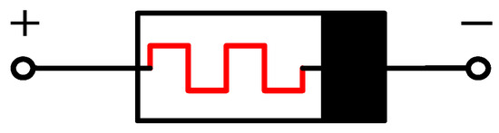
Figure 1.
The memristor symbol.
As an important 20th century discovery, the HP memristor has attracted wide attention. However, up to now, the HP memristor has not been produced and circulated, and researchers cannot obtain the real object, which makes the simulation research of memristor more important. Therefore, the implementation of the memristor model on FPGA with many resources will be of great significance to the further study of memristors.
3. Field Programmable Gate Array (FPGA) Implementation of the Threshold Memristor
According to the second part of the HP memristor threshold characteristics, this paper establishes the corresponding memristor model in FPGA, as shown in Figure 2. In order to highlight the characteristics of the memristor as a bipolar memory device in Quartus II as show in Figure 1, two input terminals InP and InN need to be designed in this model; concretely, InP represents the positive memristor input electrode while InN represents the negative memristor input electrode. One output terminal Rout is needed to be established to show the corresponding value of the memristor. The 8-bit binary numbers InP [7..0], InN [7..0] and Rout [7..0] are used to represent the forward input voltage, reverse input voltage, and the memristance of the memristor at each voltage, respectively. The data in this design are set to be 8-bit binary number, to ensure the needs of the subsequent computing module, because fewer bits are possible to make overflow during calculation.
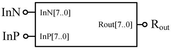
Figure 2.
The threshold memristor model based on Verilog HDL.
According to the analysis in the previous section, when VInP > VInN, the memristor is in the forward conducting state, and the memristor’s value is RON, then Rout [7..0] = 00000000; on the contrary, Rout [7..0] = 11111111, which means that the memristor resistance value is ROFF; when VInP = VInN, Rout [7..0] = 00001111, which means the memristance does not change.
The simulation results of the threshold memristor model based on Verilog HDL are shown in Figure 3. When InP = InN = 00000000 or InP = InN =11111111, the result is Rout = 00001111, which indicate that the memristance does not change when the two input voltage are same. When InP = 00,000,000 and InN = 1111111, Rout = 11111111, that is, under the reverse voltage, the memristance value is ROFF. Conversely, when InP = 1,111,111 and InN = 00000000, Rout = 00000000, the memristor change to RON. It can be seen that the model meets the working characteristics of the threshold memristor and meets the above design requirements.
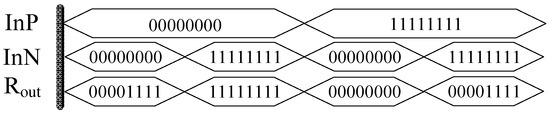
Figure 3.
Simulation waveform of the memristor model.
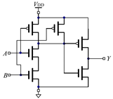
Table 1 shows two different ways of constructing an AND gate and an OR gate with the traditional CMOS method and the threshold memristor model based on FPGA we proposed in this paper. From Table 1, we can see that the traditional CMOS based AND gates and OR gates are composed of three pairs of CMOS. However, for the gates based on the threshold memristor model of FPGA we only need two memristors and one computing module, respectively. Compared with traditional CMOS-based gates, the number of components of the proposed circuit is significantly reduced, and the memristor itself has advantages in both size and power consumption, so the corresponding gates composed of memristors are smaller in size and consume less power. Besides, because memristors are compatible with the CMOS technology, so the memristor based compound logic circuits such as NAND gate and NOR gate can be obtained by using CMOS NOT gates, and then combined logic circuits, such as adders, decoders and encoders can be realized too.

Table 1.
Comparison between gates based on traditional CMOS gates and threshold memristor gates built in FPGA.
4. FPGA Implementation of Memristor Basic Logic Gate Circuit
4.1. Design of AND Gate and OR Gate Based on Memristor
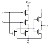
In order to realize the memristor based AND gate, the positive terminals of the two memristors need to be connected and led out as the output terminals of the AND gates, and the two negative ends are, respectively, used as the input signal terminals [19], as shown in Figure 4a. When both input terminals are at a high level, the output is also at a high level; when both input terminals are low, the output is also low. When the input at both ends is different, the corresponding output of the AND gate is calculated according to the principle of voltage dividing. For example, when VAND1 is at high level, VH = VDD, and VAND2 is at low level, VL = 0 V, the current in the circuit will flow from high voltage level to low voltage level. At this time, the resistance of MR1 is ROFF, and the resistance of MR2 is RON. Since ROFF >> RON, the output of the AND gate is VAND_O and is determined by the voltage divided by the two memristors, as shown in Equation (1). Because of the symmetry of the circuit, the same result is obtained when the input level is switched.
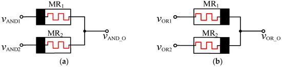
Figure 4.
Models of AND and OR gates for the memristor: (a) memristor AND gate; (b) memristor OR gate.
The OR gate design based on the memristor is similar to the AND gate mentioned above, but the difference is that the negative ends of the two memristors need to be connected and led out as the output terminals and the two positive terminals as the input terminals, as shown in Figure 4b. The working principle of the two gates is similar, and the voltage dividing principle is used to complete the calculation. The current flow direction in the circuit is from high voltage level to low voltage level. In the case of VOR1 = VH = VDD, VOR2 = VL = 0 V, according to the working characteristics of the memristor, MR1 shows low resistance RON, MR2 presents high resistance ROFF, and the voltage distribution of two memristors determines the output VOR_O. The value of VOR_O is shown in Equation (2). The circuit model has a symmetrical structure, so the same result is obtained when the input conditions are exchanged.
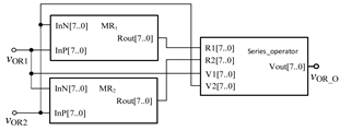
4.2. Implementation of AND Gate and OR Gate Based on Memristor in FPGA
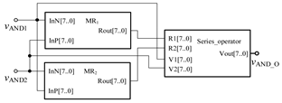
From the above analysis, to realize the memristor based AND gate and OR gate circuit through FPGA, the two memristors need to be designed in series. Therefore, it is necessary to design a basic operation module to simulate the operation in the actual circuit, as shown in Figure 5. Among them, the input terminals R1 and R2 are, respectively, connected with the output terminals of the two memristors in series, that is, the memristor values Rout1 and Rout2 of the two memristors; the input terminals V1 and V2 are respectively connected with the two input terminals of the series circuit; the output of the module is the voltage value VOUT at the two memristors in series. The module can distinguish whether each memristor is currently in forward bias or reverse bias by the value of V1 and V2, so as to obtain the memristor values of the two memristors under the input voltage, and assign the values to R1 and R2, and calculate according to Equation (3) to obtain the corresponding output value.
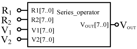
Figure 5.
Serial module based on Verilog HDL.
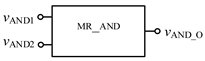
In order to verify the correctness of the design, the threshold memristor designed in the previous section and the series operation module established in this section can be used in Quartus II, and the simulation circuit of the AND gate is shown in Figure 6. The negative inputs of the two memristors are used as the input terminals of the whole AND gate, and the Rout outputs the memristor state according to the level of the input terminal. Then, the output of the whole AND gate is further obtained after the operation of the operation module according to Equation (3). The simulation results are shown in Figure 7. When both VAND1 and VAND2 are high level “11111111” or both are low level “00000000”, the output VAND_O is the same as the input. When VAND1 and VAND2 input different values, the output result represents the low level of 00000000. Therefore, the AND gate circuit designed in this paper is effective. Figure 8 shows the module diagram of the AND gate logic circuit after encapsulation.
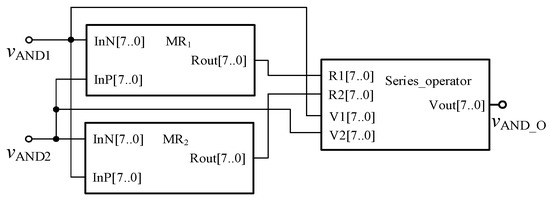
Figure 6.
AND gate circuit based on memristor.
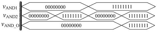
Figure 7.
Waveform of memristor AND gate circuit.
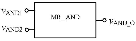
Figure 8.
AND gate module after encapsulation.
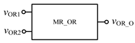
Similarly, in order to verify the effectiveness of OR gate circuit, the simulation circuit of OR gate is established as shown in Figure 9. The simulation results of Quartus II are shown in Figure 10, and Figure 11 is the module diagram after encapsulation of the OR gate logic circuit. It can be seen from the waveform simulation diagram of the OR gate in Figure 10 that when the input VOR1 and VOR2 are both high or both low, the voltage across the memristor is the same, and the output is the same as the input. When VOR1 and VOR2 are different input values, the output result is high level. Therefore, the OR gate designed in this paper is effective.
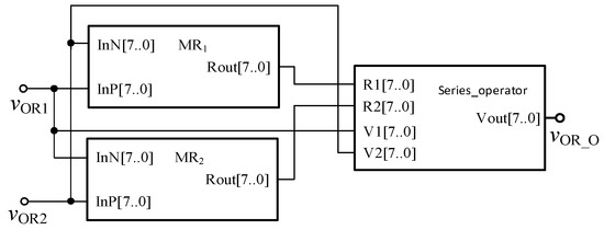
Figure 9.
The OR gate circuit based on memristor.
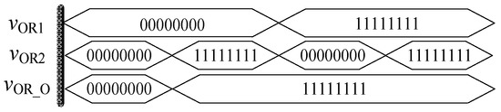
Figure 10.
Waveform of the memristor OR gate circuit.
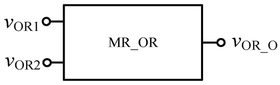
Figure 11.
OR gate module after encapsulation.
4.3. Design of FPGA Combinational Logic Gate Based on Memristor
In order to realize the memristor NAND gate and NOR gate in FPGA, this paper realizes the memristor NAND and NOR gates by connecting the NOT gate in FPGA after the AND gate and OR gate, as shown in Figure 12.
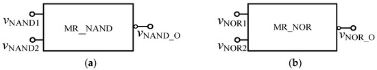
Figure 12.
Memristor NAND and memristor NOR gate: (a) encapsulated NAND gate module; (b) encapsulated NOR gate module.
4.3.1. XNOR Gate Based on Memristor in FPGA
Based on the relationship between NOR and XNOR logic gates as shown in Equation (4), the XNOR circuit based on the memristor in FPGA as shown in Figure 13 can be obtained, and the encapsulated module is shown in Figure 14.
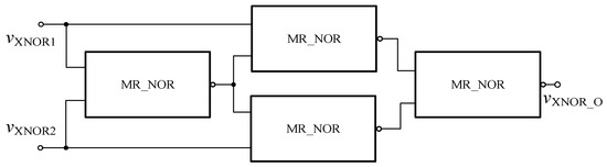
Figure 13.
Memristor XNOR gate based on Verilog HDL.
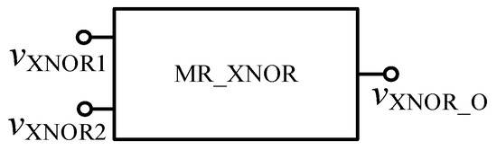
Figure 14.
The XNOR gate after encapsulation.
In order to verify the functionality of the module, circuit simulation is carried out in Quartus II software, and the simulation waveform is shown in Figure 15. When the input signals vXNOR1 and vXNOR2 are both at high level or both at low level, the output result vXNOR_O is at high level. When the input signals are different, the output result is at low level. It can be seen that the above results fully confirm with the logic function of the XNOR gate.
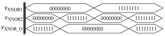
Figure 15.
Waveform of the memristor XNOR gate.
4.3.2. XOR Gate of FPGA Based on Memristor
The FPGA XOR gate based on the memristor can be composed of the memristor AND gate, OR gate and NAND gate, and can be realized according to Equation (5). The specific circuit is shown in Figure 16, and the encapsulated model is shown in Figure 17.
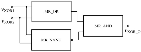
Figure 16.
Memristor XOR gate based on Verilog HDL.
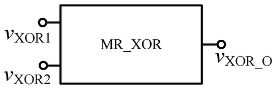
Figure 17.
The memristor XOR gate after encapsulation.
Through the simulation experiment of the above circuit, the experimental results shown in Figure 18 were obtained. It can be seen that these results are just opposite to the XNOR gate based on the memristor, that is, when the input signals vXOR1 and vXOR2 are the same, the output of vXOR_O is at a low level, and the result is at a high level when the input signals are different. This exactly conforms to the logic function of the XOR gate, and also satisfies the rule that XNOR and XOR complement each other.
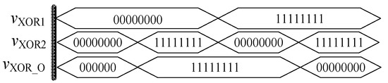
Figure 18.
Waveform of the memristor XOR gate.
5. Design of Adder Based on Memristor
In a modern computer or digital signal processing system, the operation of data is inseparable from arithmetic logic components, which can perform the logic operation, shift or command call. As one of the most important devices, the adder can complete the addition operation between two numbers, which is the basic unit of the arithmetic unit. In the hardware implementation of various digital systems, the power consumption, running speed and size of adders directly affect the design and implementation of digital systems. Therefore, the design of high-speed and low-power adder circuit is of great significance to a digital system. A memristor has the advantages of fast operation, small size, and low power consumption. The application of the memristor in an adder circuit can greatly improve the performance of the adder. In this section, half adder and full adder are implemented in FPGA by using the logic gates based on memristor.
5.1. Half Adder Design
The half adder is the simplest addition circuit. It adds two 1-bit binary numbers A and B to produce sum S and carry CO. The output expression of the half adder is shown in Equation (6), that is, it is composed of an XOR gate and an AND gate. In this paper, a half adder circuit is realized using a memristor-based XOR gate and AND gate shown in Figure 19. Since the carry from low bit is not considered in addition here, the circuit shown in Figure 19 can only be called a half adder, and the encapsulated module is shown in Figure 20.
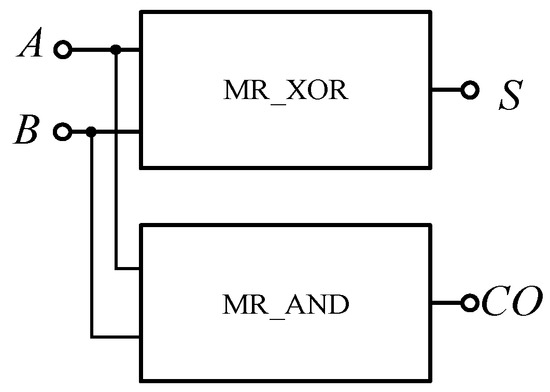
Figure 19.
Half adder based on memristor.
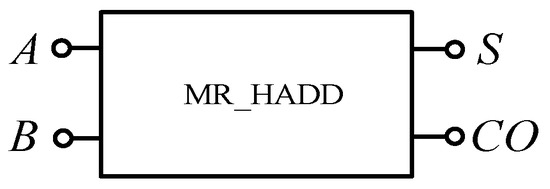
Figure 20.
The half adder after encapsulation.
Through the establishment of a simulation circuit in Quartus II, the half adder function is tested, and the simulation results as shown in Figure 21 are obtained. In the figure, 000,000,000 is equivalent to 1-bit binary data “0”, 11,111,111 is equivalent to 1-bit binary data “1”. When two addends A and B are “0”, then S and carry CO are both “0”; when one of the two addends A and B is “0” and the other is “1”, carry CO is “0”; when two addends A and B are “0”, carry CO is “0” When A and B are “1”, then S and carry CO are “1”, the design conforms to the logic rules of a half adder.
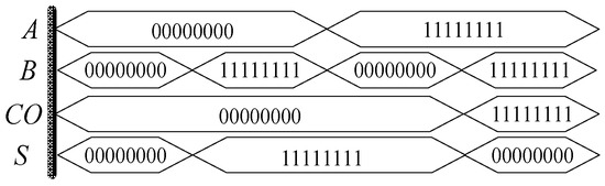
Figure 21.
Waveform of the half adder based on memristor.
5.2. Full Adder Design
A logic circuit that adding two binary numbers and considering carry from the low bit to the high bit is called the full adder. The full adder not only considers the addition of two binary numbers, but also takes the carry from the low bit into the addition operation. The expression of the full adder is shown in Equation (7), where A and B are addends, C is the carry digit of the low order, S is the standard sum value, and CO is the carry forward to the high order.
The full adder circuit can be constructed with the memristor-based AND gate, OR gate and XOR gate according to Equation (7), as shown in Figure 22. It can also be composed of two half adders and one OR gate. Figure 23 shows a full adder circuit composed of memristor-based half adders.
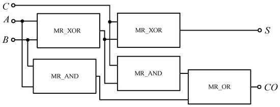
Figure 22.
Full adder circuit based on memristor XOR gate, AND gate and OR gate.
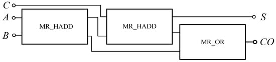
Figure 23.
Full adder circuit based on memristor half adders.
Figure 24 shows the simulation circuit results of a full adder based on a memristor built in Quartus II software. Similar to the half adder, 00,000,000 is equivalent to 1-bit binary data “0”, and 11,111,111 is equivalent to 1-bit binary data “1”. When A, B and C of the full adder are all “0”, the standard S and carry CO of the output end are all “0”; when any one of A, B and C is “1” and the other two are “0”, then S is “1” and carry CO is “0”; when any one of A, B and C is “0” and the other two are “1”,then S is “0” and carry CO is “1”; when A, B and C are all “1”, then S is “0”, carry CO is “1”; when A, B and C are “1”, then S is “0”, and carry CO is “0” when A, B and C are all “1”, then S is “1”, and CO is “1”. The design conforms to the logic rules of a full adder.
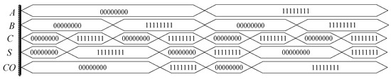
Figure 24.
Waveform of the full adder based on memristor.
6. Conclusions
In this paper, the circuit model of a threshold memristor is established in FPGA, and the AND gate and OR gate circuits based on the memristor are realized by using this model. Combined with the NOT gate circuit in FPGA, the NAND gate, NOR gate, XOR gate and the XNOR gate based on the memristor are further realized, and the adder is designed based on the above gate circuits. Logic devices are widely used in digital systems. With the development of modern digital technology towards small size, low power consumption and high speed, compared with traditional CMOS circuits, memristor-based logic circuits can not only increase the density of devices, but also reduce the power consumption of circuits, and improve the operation speed of circuits. The emergence of such devices will inevitably bring about great changes in digital technology.
Author Contributions
Conceptualization, X.W., L.Y. and Y.W.; data curation, X.W., L.Y. and Y.W.; investigation, X.W. and L.Y.; methodology, X.W. and L.Y.; resources, L.Y., Y.W., Z.W. and X.W.; writing—original draft, L.Y., Y.W. and X.W.; and writing—review and editing, L.Y., Z.W. and X.W. All authors have read and agreed to the published version of the manuscript.
Funding
This research was funded by the National Natural Science Foundation of China, grant number 61871429 and the Natural Science Foundation of Zhejiang Province, grant number LY18F010012, and the Fundamental Research Funds for the Provincial Universities of Zhejiang, grant number GK219909299001-413.
Data Availability Statement
No new data were created or analyzed in this study. Data sharing is not applicable to this article.
Conflicts of Interest
The authors declare no conflict of interest.
References
- Chua, L.O. Memristor-The missing circuit element. IEEE Trans. Circuit Theory 1971, 18, 507–519. [Google Scholar] [CrossRef]
- Strukov, D.B.; Snider, G.S.; Stewart, D.R. The missing memristor found. Nature 2008, 453, 80–83. [Google Scholar] [CrossRef] [PubMed]
- Chua, L.O. Resistance switching memories are memristors. Appl. Phys. A Mater. Sci. Process. 2011, 102, 765–783. [Google Scholar] [CrossRef] [Green Version]
- Borghetti, J.; Snider, G.S.; Kuekes, P.J. Memristive switches enable ’stateful’ logic operations via material implication. Nature 2010, 464, 873–876. [Google Scholar] [CrossRef] [PubMed]
- Kvatinsky, S.; Wald, N.; Satat, G. MRL-Memristor Ratioed Logic. In Proceedings of the Cellular Nanoscale Networks and Their Applications (CNNA) 2012 13th International Workshop, Turin, Italy, 29–31 August 2012. [Google Scholar]
- Vourkas, I.; Sirakoulis, G.C. Emerging Memristor-Based Logic Circuit Design Approaches: A Review. IEEE Circuits Syst. Mag. 2016, 16, 15–30. [Google Scholar] [CrossRef]
- Lehtonen, E.; Tissari, J.; Poikonen, J.; Laiho, M.; Koskinen, L. A cellular computing architecture for parallel memristive stateful logic. Microelectron. J. 2014, 45, 1438–1449. [Google Scholar] [CrossRef]
- Mane, P.; Talati, N.; Riswadkar, A.; Jasani, B.; Ramesha, C.K. Implementation of NOR logic based on material implication on CMOL FPGA architecture. In Proceedings of the 2015 28th International Conference on VLSI Design, Bangalore, India, 3–7 January 2015; pp. 523–528. [Google Scholar]
- Rohani, S.; Taherinejad, N. An improved algorithm for IMPLY logic based memristive full-adder. In Proceedings of the 2017 IEEE 30th Canadian Conference on Electrical and Computer Engineering, Windsor, ON, Canada, 30 April–3 May 2017; pp. 1–4. [Google Scholar]
- Kvatinsky, S.; Belousov, D.; Liman, S. MAGIC-Memristor-aided logic. IEEE Trans. Circuits Syst. II Express Briefs 2014, 61, 895–899. [Google Scholar] [CrossRef]
- Liu, P.; You, Z.; Kuang, J.; Hu, Z.; Wang, W. Logic operation-based DFT method and 1R memristive crossbar march-like test algorithm. Inst. Electron. Inf. Commun. Eng. 2015. [Google Scholar] [CrossRef] [Green Version]
- Thangkhiew, P.; Gharpinde, R.; Chowdhary, P.V.; Datta, K.; Sengupta, I. Area efficient implementation of ripple carry adder using memristor crossbar arrays. In Proceedings of the 2016 11th International Design & Test Symposium (IDT) IEEE, Hammamet, Tunisia, 18–20 December 2016. [Google Scholar]
- Lin, C.; Zhong, H.; Wang, X.; Zeng, Z. Several Logic Gates Extended from MAGIC-Memristor-Aided Logic. In International Symposium on Neural Networks; Springer: Berlin/Heidelberg, Germany, 2017; pp. 170–179. [Google Scholar]
- Thangkhiew, P.; Gharpinde, R.; Datta, K. Efficient Mapping of Boolean Functions to Memristor Crossbar Using MAGIC NOR Gates. IEEE Trans. Circuits Syst. I Regul. Pap. 2018, 8, 2466–2476. [Google Scholar] [CrossRef]
- Chakraborty, A.; Saurabh, V.; Gupta, P.S.; Kumar, R.; Majumdar, S.; Das, S.; Rahaman, H. In-memory designing of delay and toggle flip-flops utilizing memristor aided logic (MAGIC). Integr. VLSI J. 2018, 66, 24–34. [Google Scholar] [CrossRef]
- Teimoori, M.; Ahmadi, A.; Alirezaee, S.; Ahmadi, M. A novel hybrid CMOS-memristor logic circuit using Memristor Ratioed Logic. In Proceedings of the 29th Annual IEEE Canadian Conference on Electrical and Computer Engineering, Vancouver, BC, Canada, 15–19 May 2016. [Google Scholar]
- Xu, X.; Cui, X.; Luo, M.; Luo, M.; Lin, Q.; Luo, Y.; Zhou, Y. Design of hybrid memristor-MOS XOR and XNOR logic gates. In Proceedings of the International Conference on Electron Devices & Solid-state Circuits, Hsinchu, Taiwan, 18–20 October 2017; pp. 1–2. [Google Scholar]
- Liu, G.; Zheng, L.; Wang, G.; Shen, Y.; Liang, Y. A carry lookahead adder based on hybrid CMOS-memristor logic circuit. IEEE Access 2019, 7, 43691–43696. [Google Scholar] [CrossRef]
- Wang, X.Y.; Zhou, P.F.; Eshraghian, J. High-density memristor-CMOS ternary logic family. IEEE Trans. Circuits Syst. I Regul. Pap. 2020, 68, 264–274. [Google Scholar] [CrossRef]
- Singh, A. Memristor based XNOR for high speed area efficient 1-bit full adder. In Proceedings of the International Conference on Computing, Silicon Valley, CA, USA, 26–29 January 2017; pp. 1549–1553. [Google Scholar]
- Ahmad, K.; Rezai, A. Novel design for a memristor-based full adder using a new IMPLY logic approach. J. Comput. Electron. 2018, 17, 1303–1314. [Google Scholar]
- Wei, Z.; Wang, Y.; Jiang, X. Design of Modular Multiplier Based on Memristor. In Proceedings of the 2019 IEEE International Workshop on Future Computing (IWOFC), Hangzhou, China, 4–15 December 2019. [Google Scholar]
- Guckert, L.; Swartzlander, E.E. Optimized Memristor-Based Multipliers. IEEE Trans. Circuits Syst. I Regul. Pap. 2017, 64, 373–385. [Google Scholar] [CrossRef]
- Teimoory, M.; Amirsoleimani, A.; Ahmadi, A. A hybrid memristor-CMOS multiplier design based on memristive universal logic gates. In Proceedings of the 2017 IEEE 60th International Midwest Symposium on Circuits and Systems (MWSCAS), Boston, MA, USA, 6–9 August 2017. [Google Scholar]
- Chakraborty, A.; Dhara, A.; Rahaman, H. Design of memristor-based up-down counter using material implication logic. In Proceedings of the International Conference on Advances in Computing, Durban, South Africa, 28–29 November 2016. [Google Scholar]
- Wang, X.; Wu, Z.; Zhou, P.; Herbert, H.C.; Iu, J.K.; Eshraghian, S.M.K. FPGA Synthesis of Ternary Memristor-CMOS Decoders. 2021. Available online: https://www.x-mol.com/paper/1385372791650410496?adv (accessed on 21 April 2021).


Publisher’s Note: MDPI stays neutral with regard to jurisdictional claims in published maps and institutional affiliations. |
© 2021 by the authors. Licensee MDPI, Basel, Switzerland. This article is an open access article distributed under the terms and conditions of the Creative Commons Attribution (CC BY) license (https://creativecommons.org/licenses/by/4.0/).