
A Novel and Cost-Effective Drive Circuit for Supplying a Piezoelectric Ceramic Actuator with Power-Factor-Correction and Soft-Switching Features

 ,
,  ,
,  ,
, 

Abstract
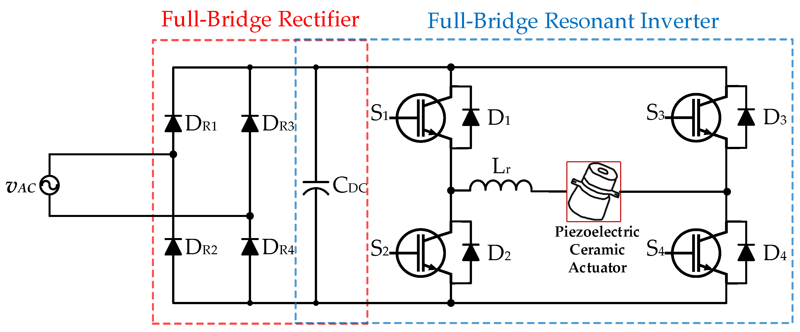
:1. Introduction
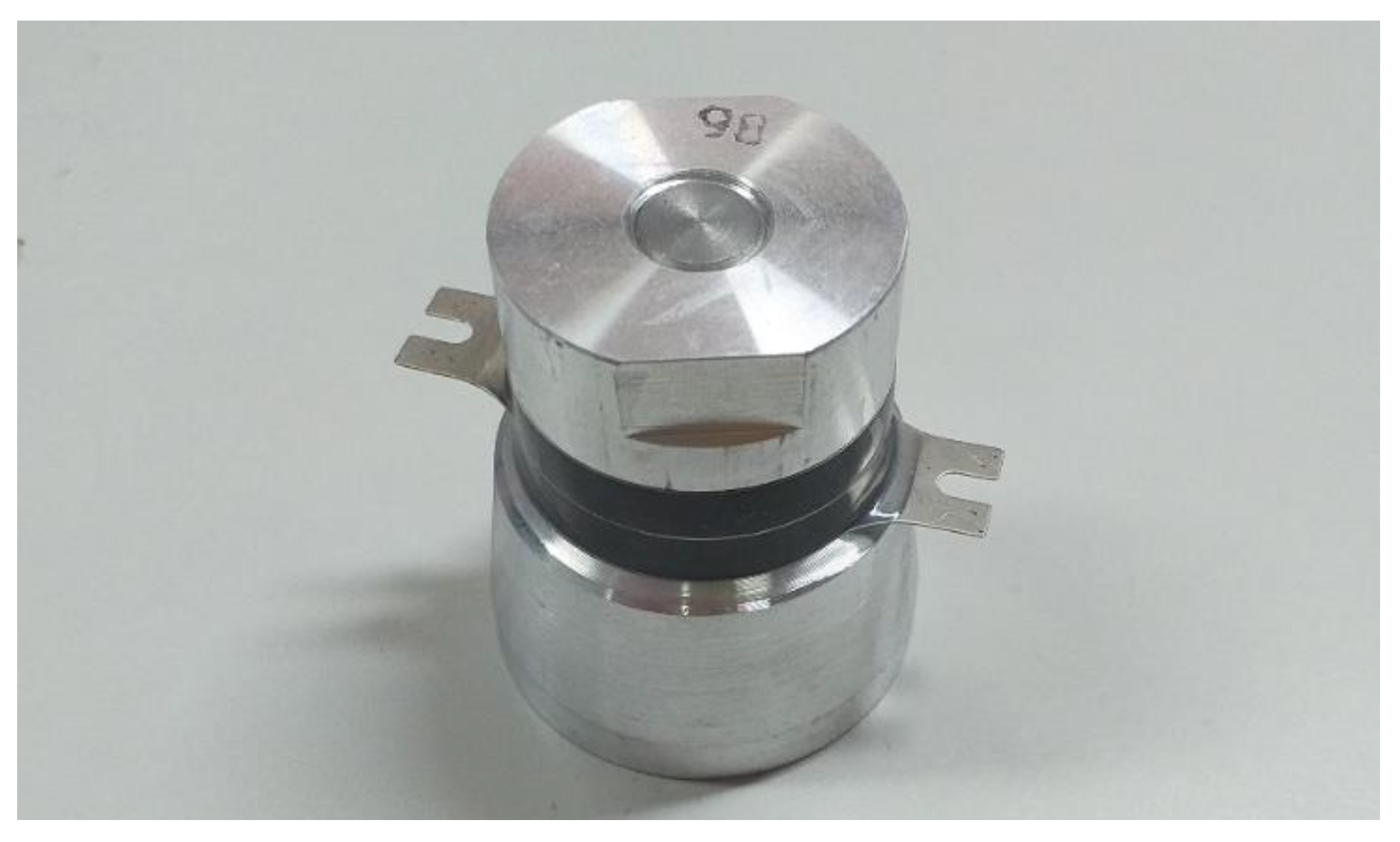
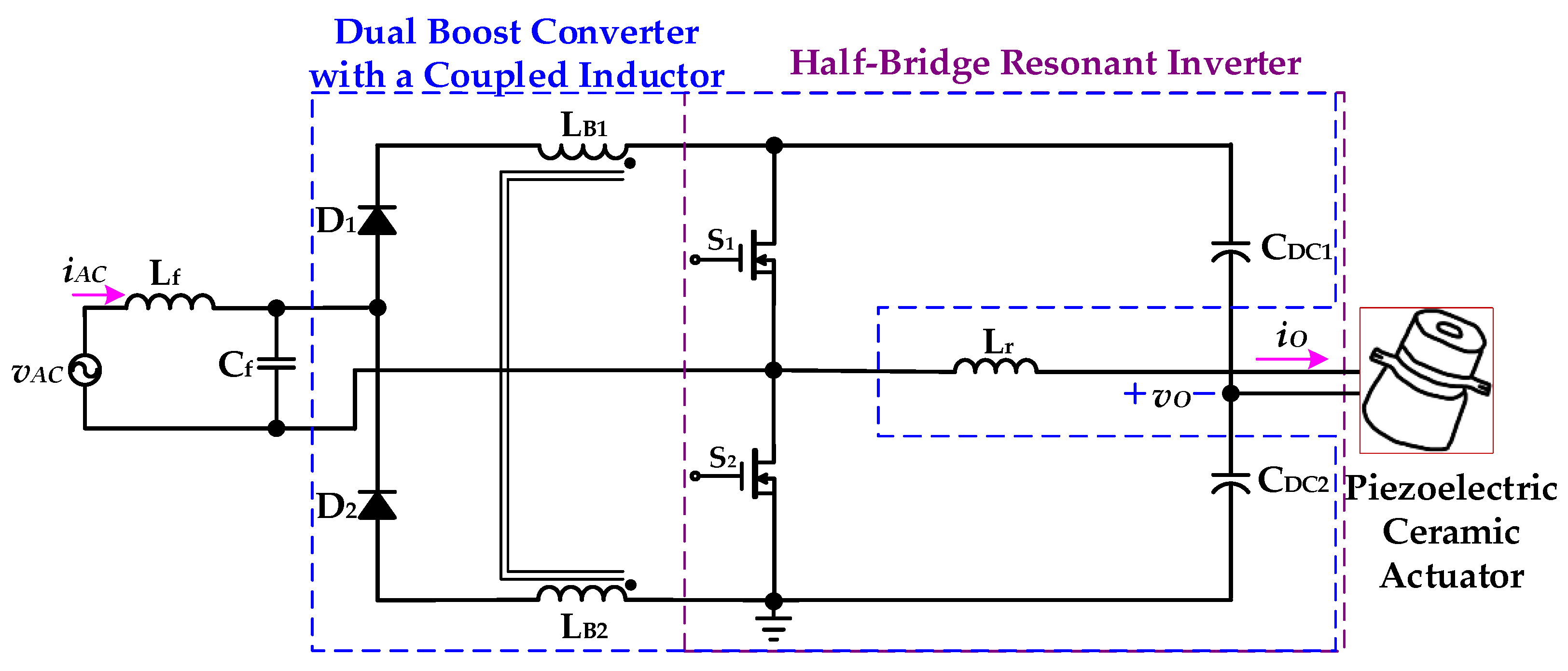
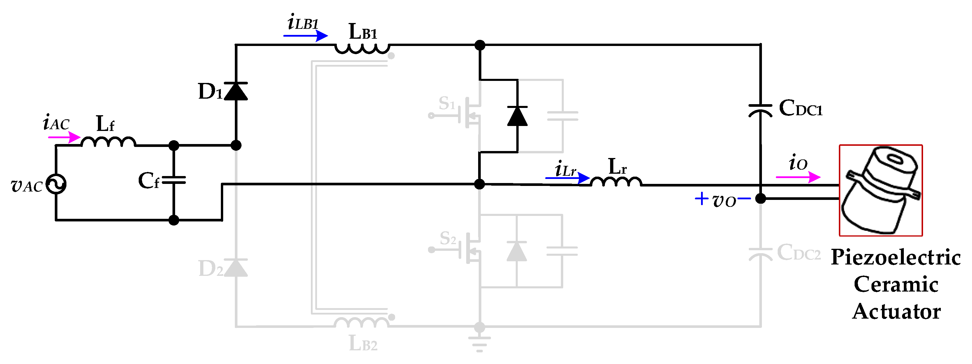
2. The Proposed Drive Circuit for Supplying a Piezoelectric Ceramic Actuator
2.1. Introduction of Proposed Drive Circuit
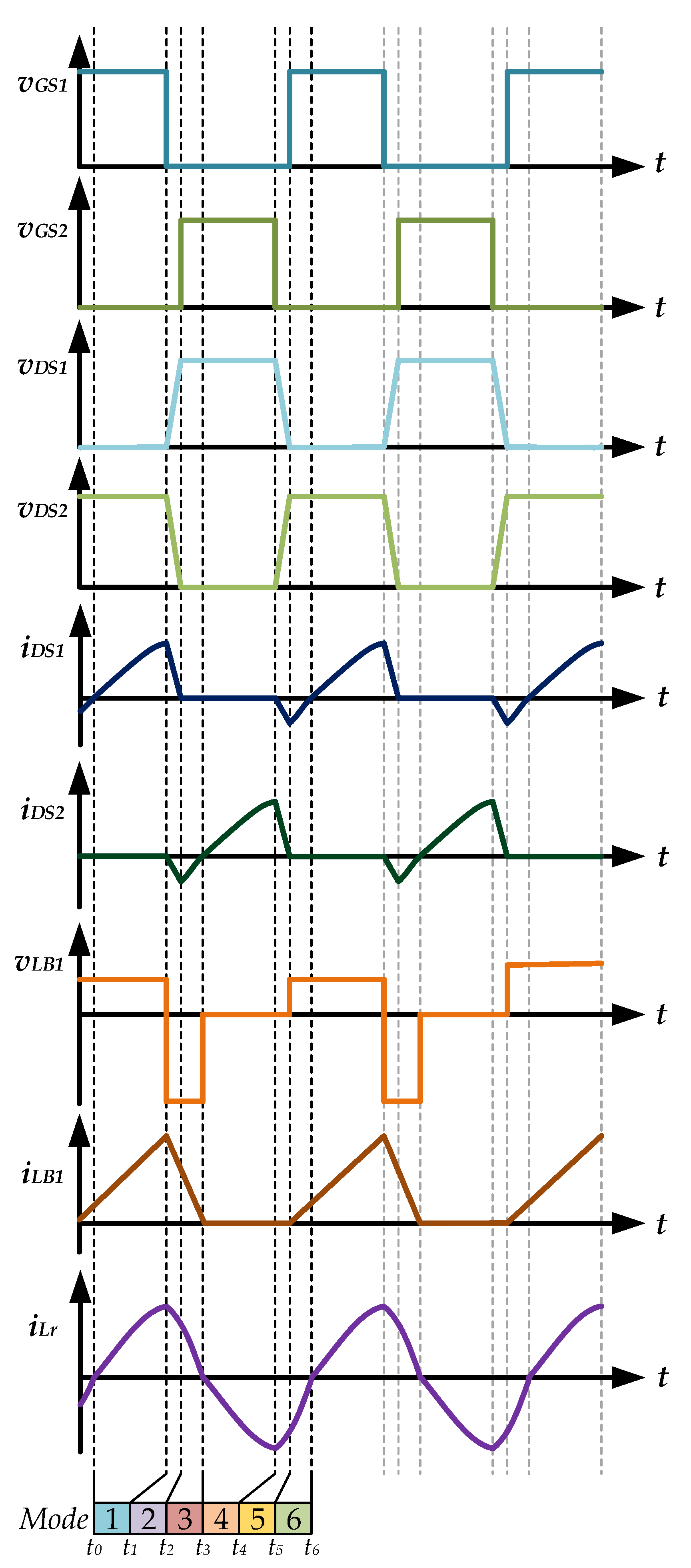
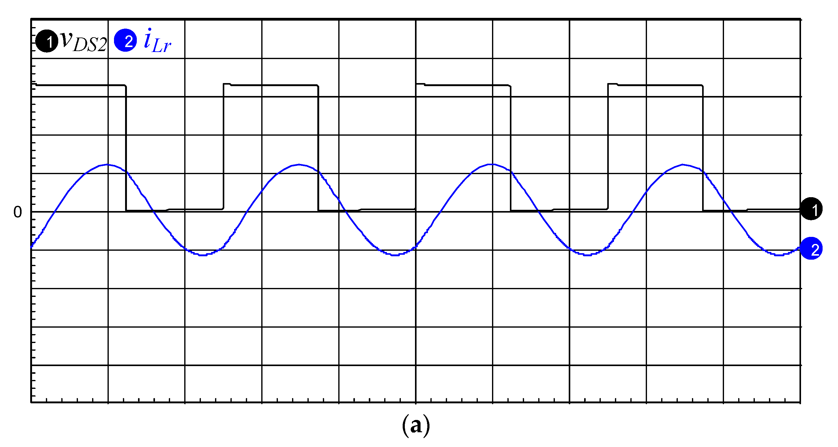
2.2. Analysis of Operational Modes
- The control signals of the power switches S1 and S2 are in a complementary state, and the essential diodes and parasitic capacitances on the power switches are considered.
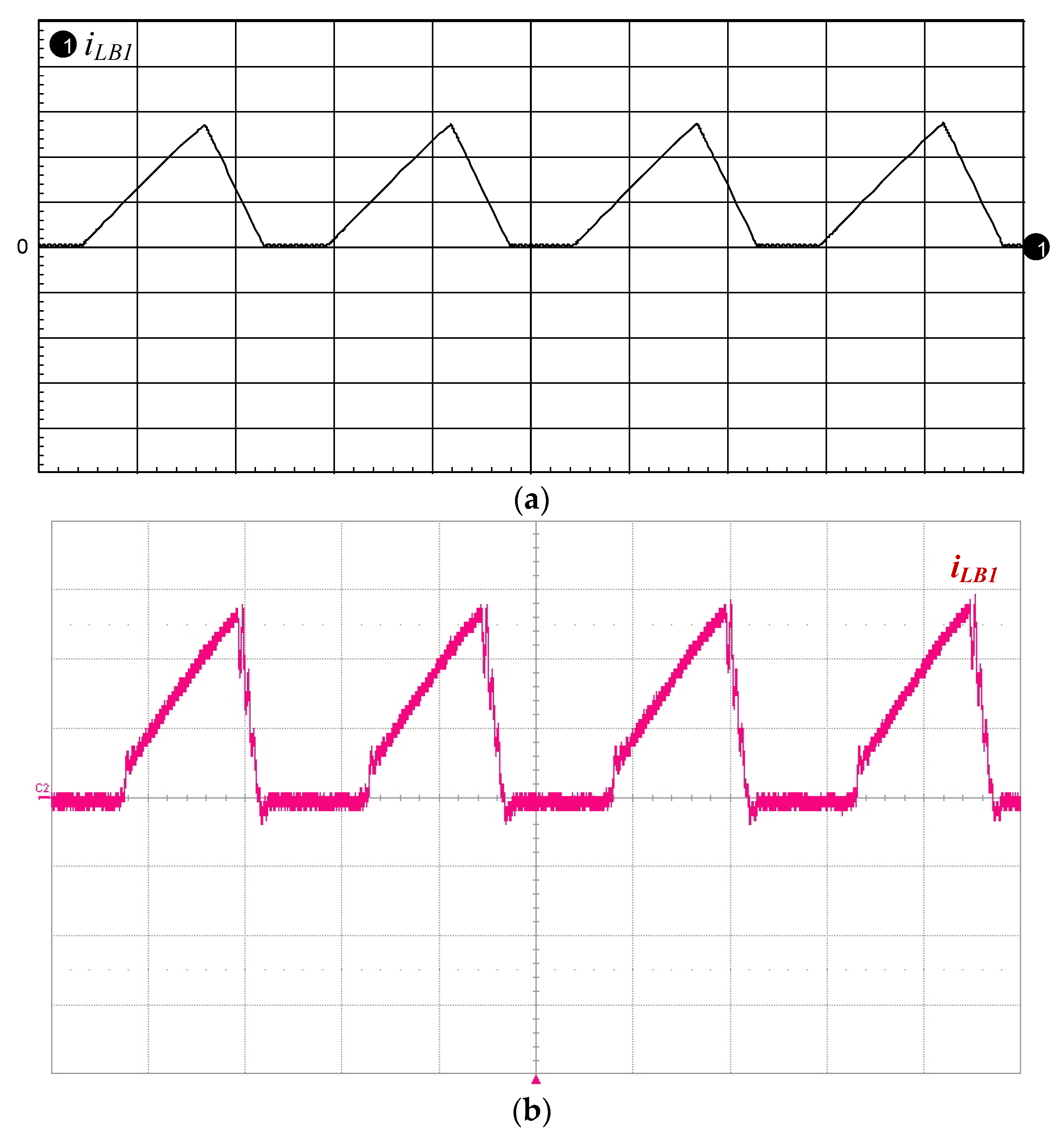
- The two coupled inductors LB1 and LB2 in the drive circuit are designed to operate in discontinuous-conduction Mode (DCM).
- The equivalent resistance of diodes D1 and D2 and the forward bias voltage drop are ignored in the analysis.
- The remaining circuit components are assumed to be ideal.
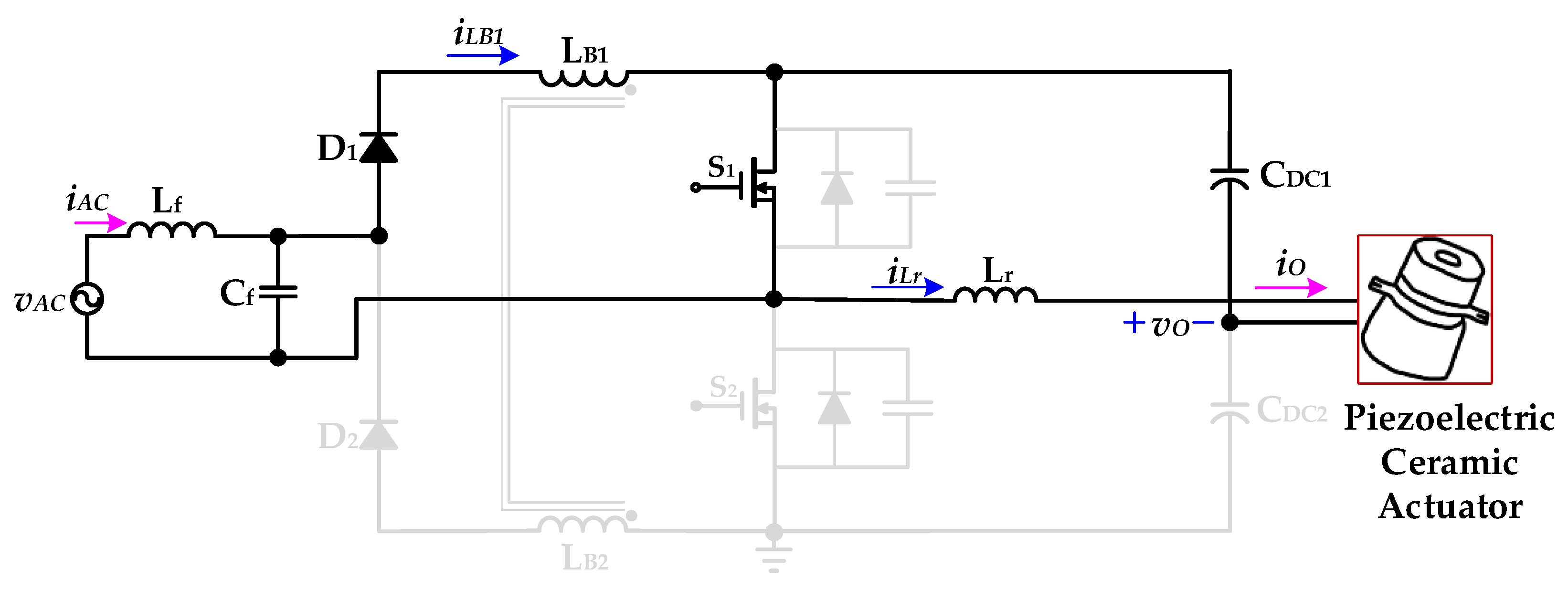
2.2.1. Operational Mode 1 (t0 ≤ t < t1)
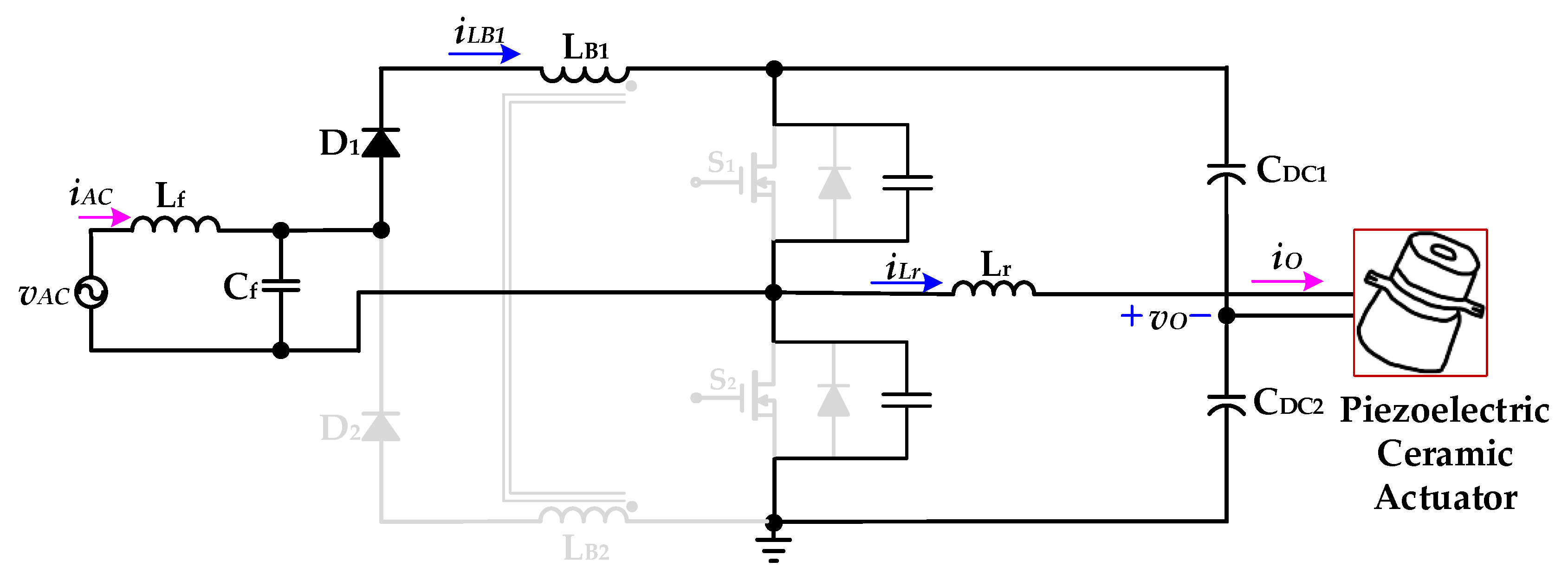
2.2.2. Operational Mode 2 (t1 ≤ t < t2)
2.2.3. Operational Mode 3 (t2 ≤ t < t3)
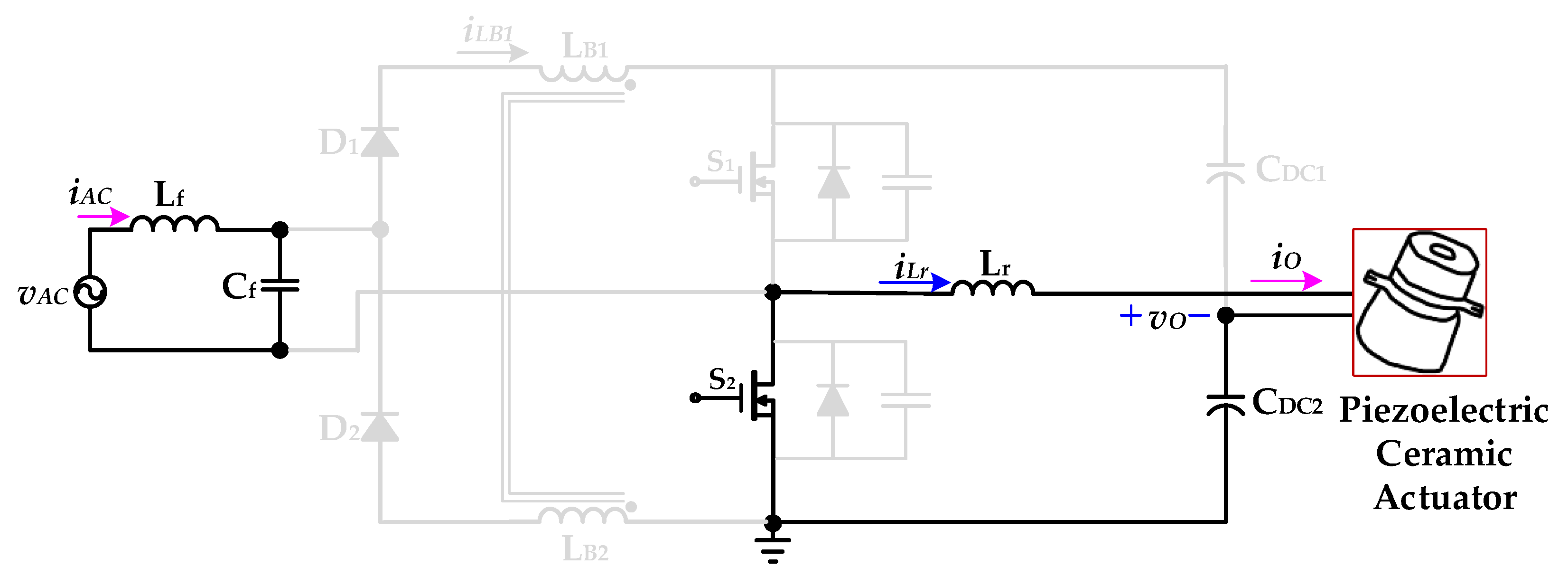
2.2.4. Operational Mode 4 (t3 ≤ t < t4)
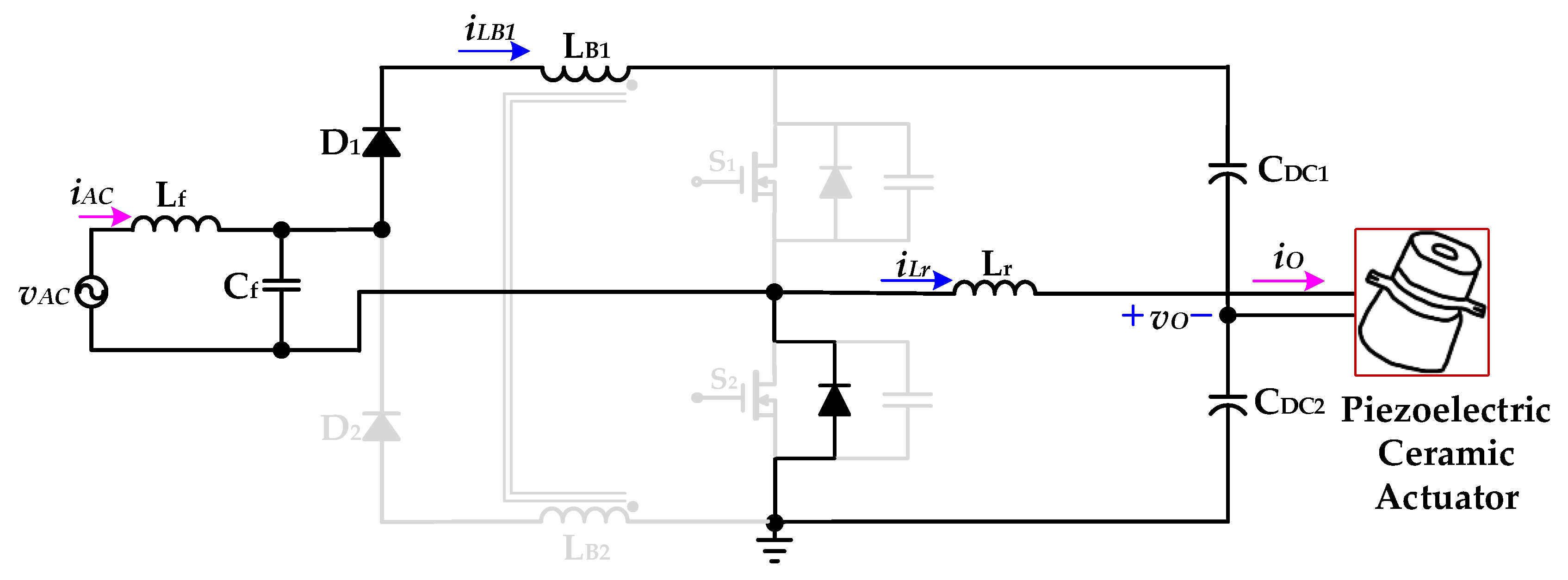
2.2.5. Operational Mode 5 (t4 ≤ t < t5)
2.2.6. Operational Mode 6 (t5 ≤ t < t6)
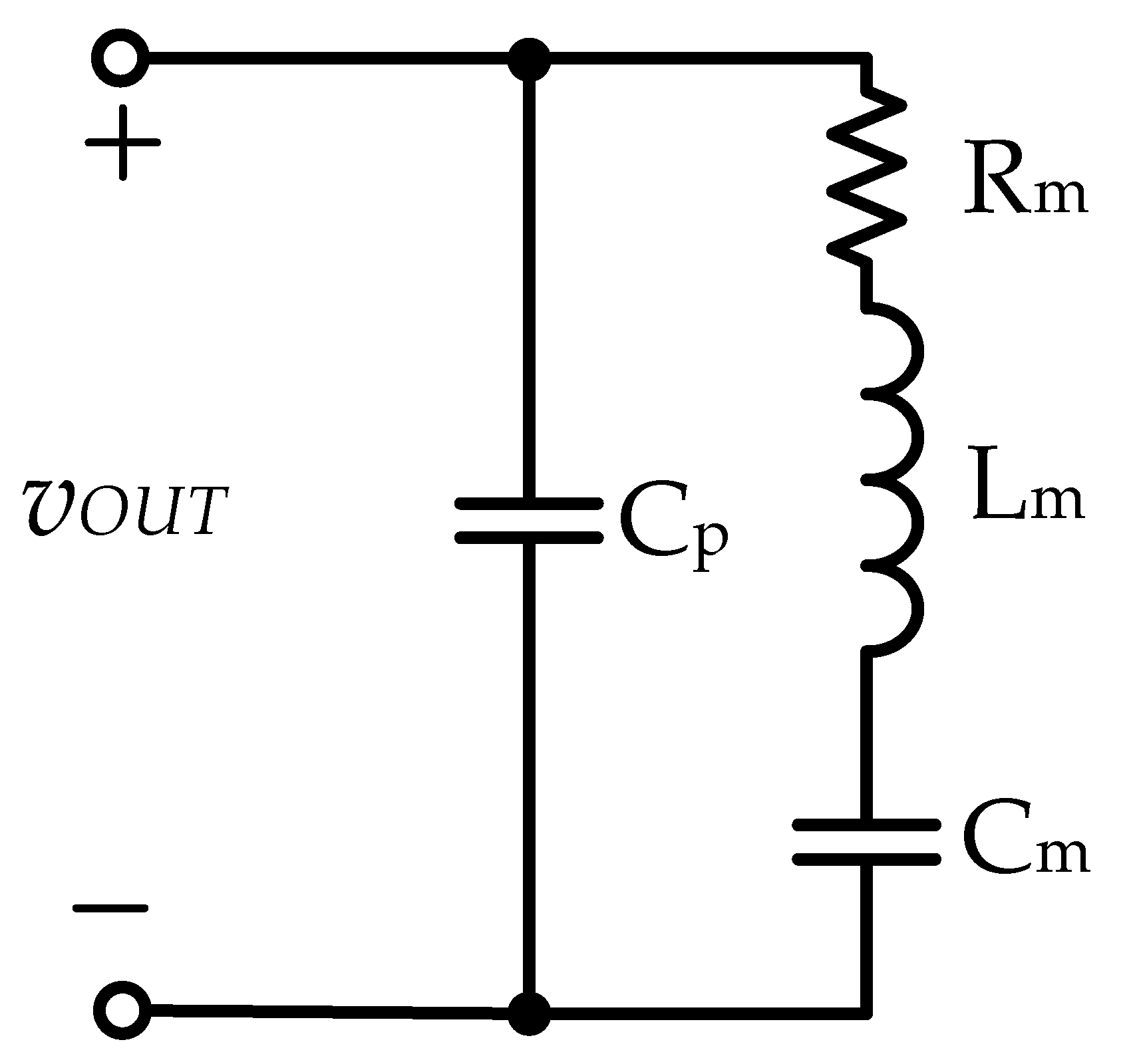
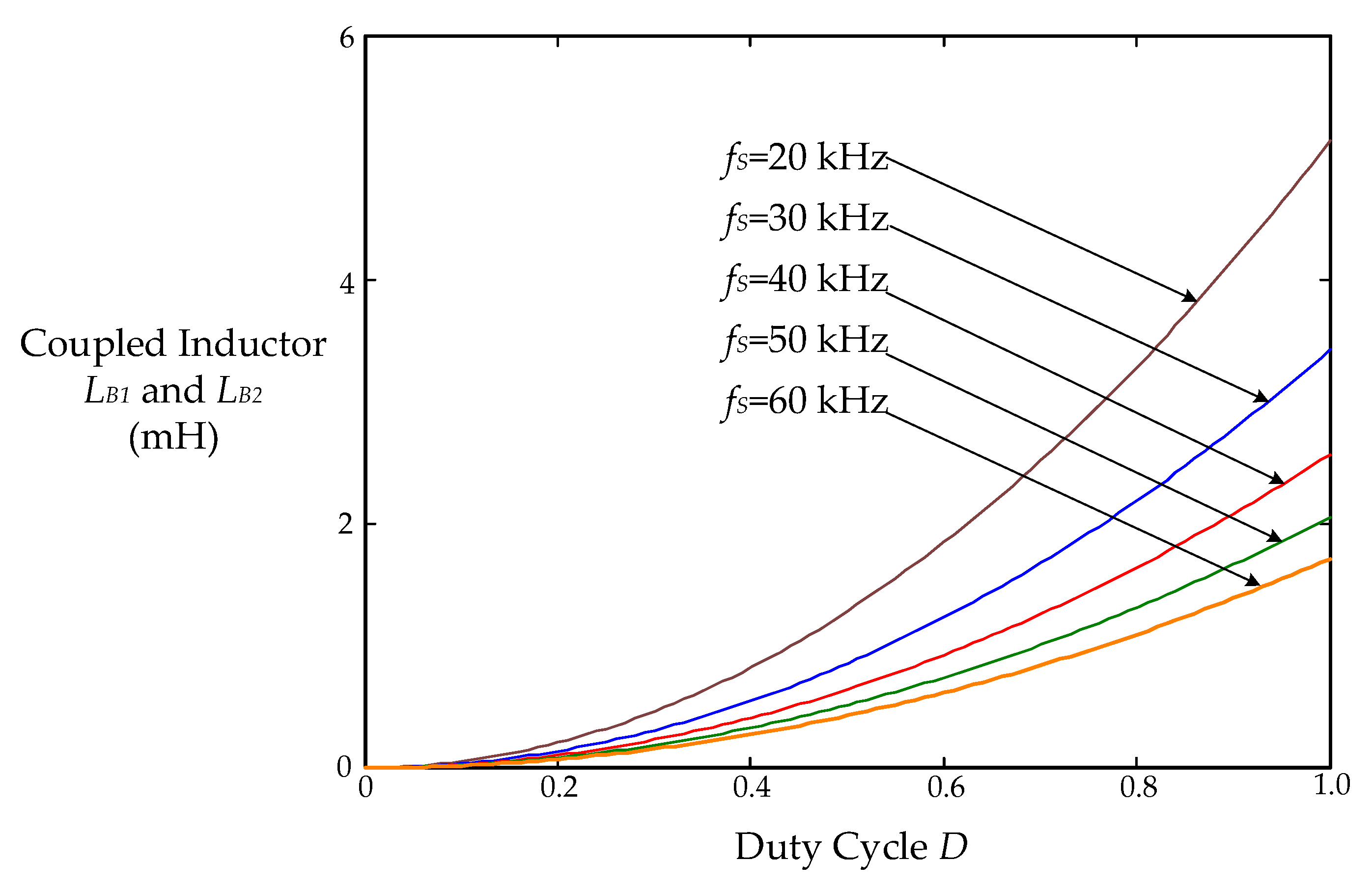
2.3. Design Equations of Key Circuit Parameters
2.3.1. Design Equation of the Coupled Inductors LB1 and LB2
2.3.2. Design Equation of the Resonant Inductor Lr
2.3.3. Design of Input Low-Pass Filter
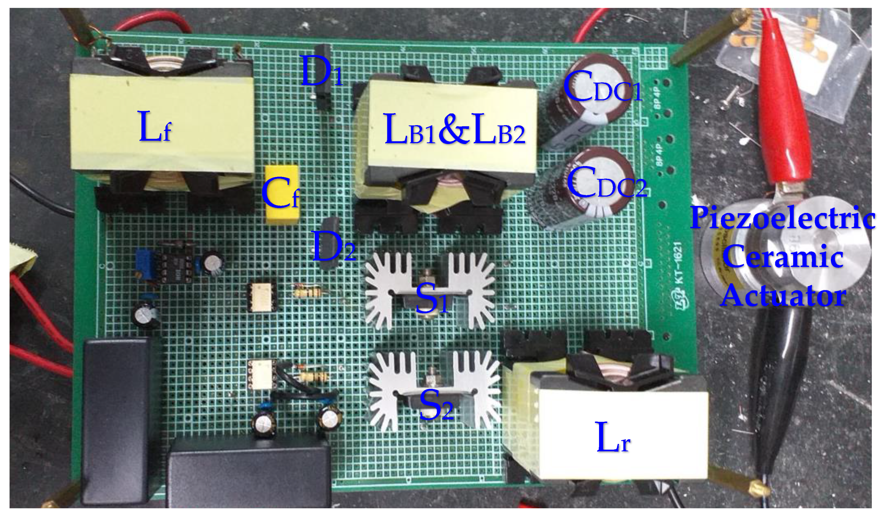
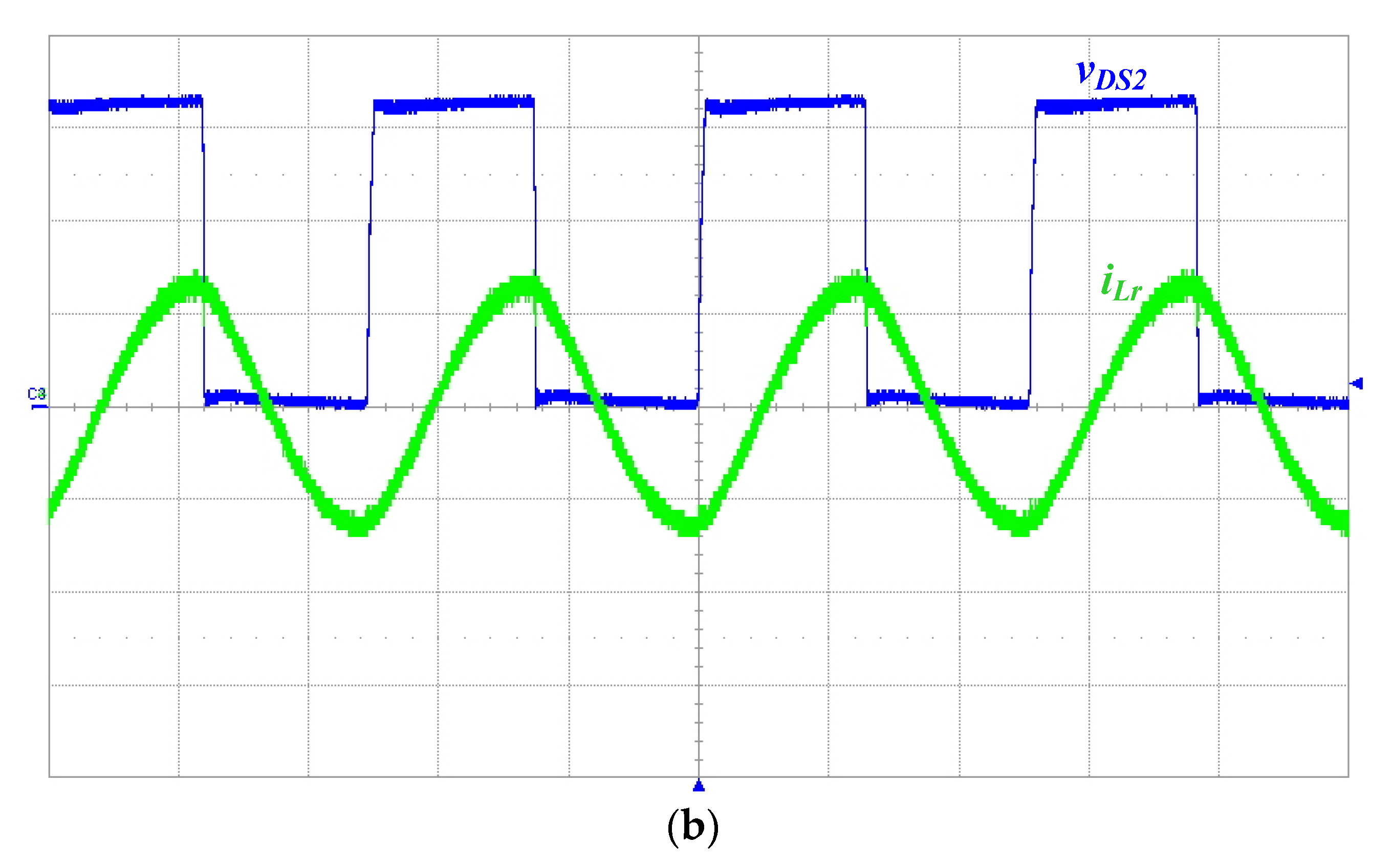
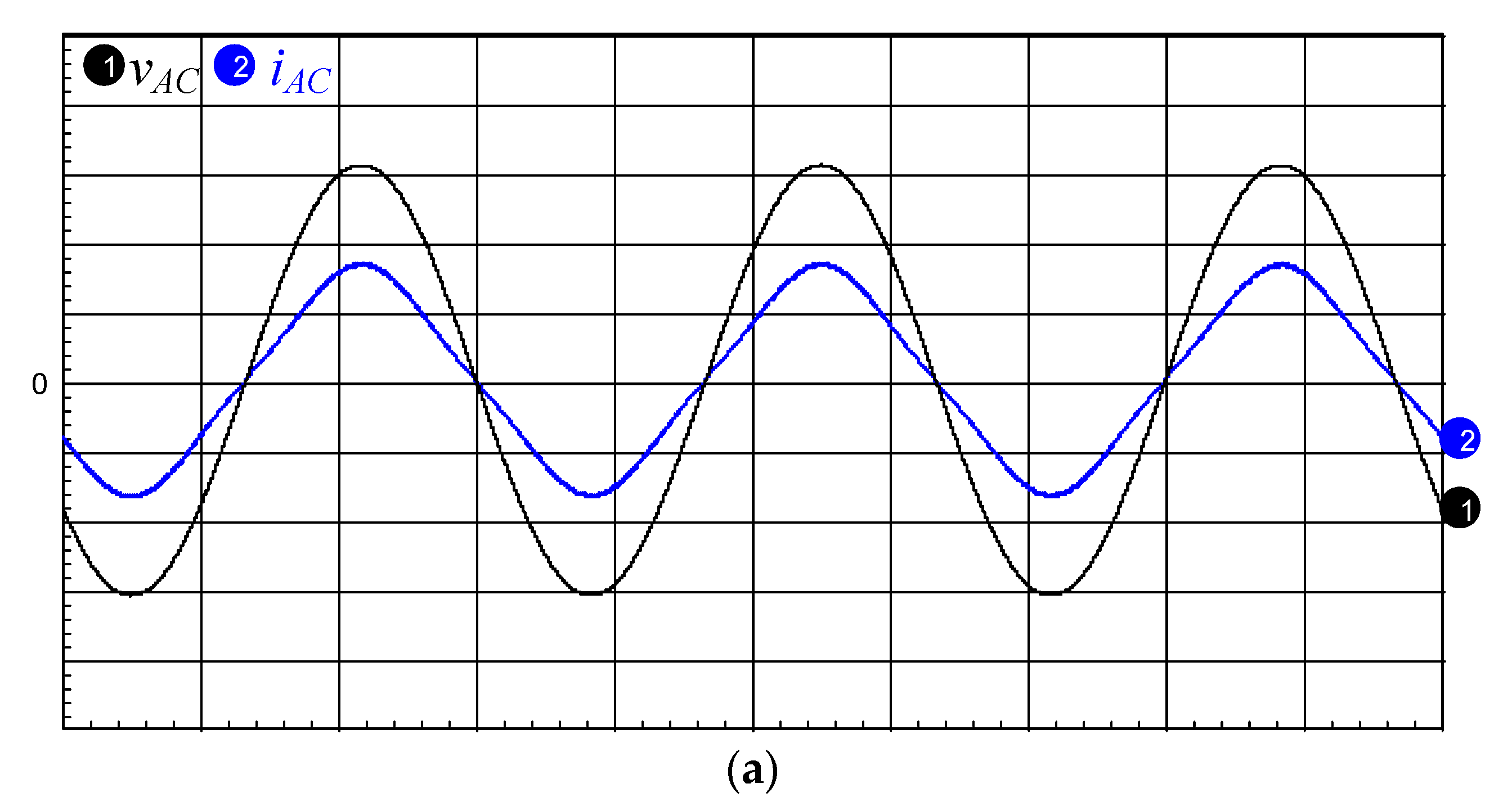
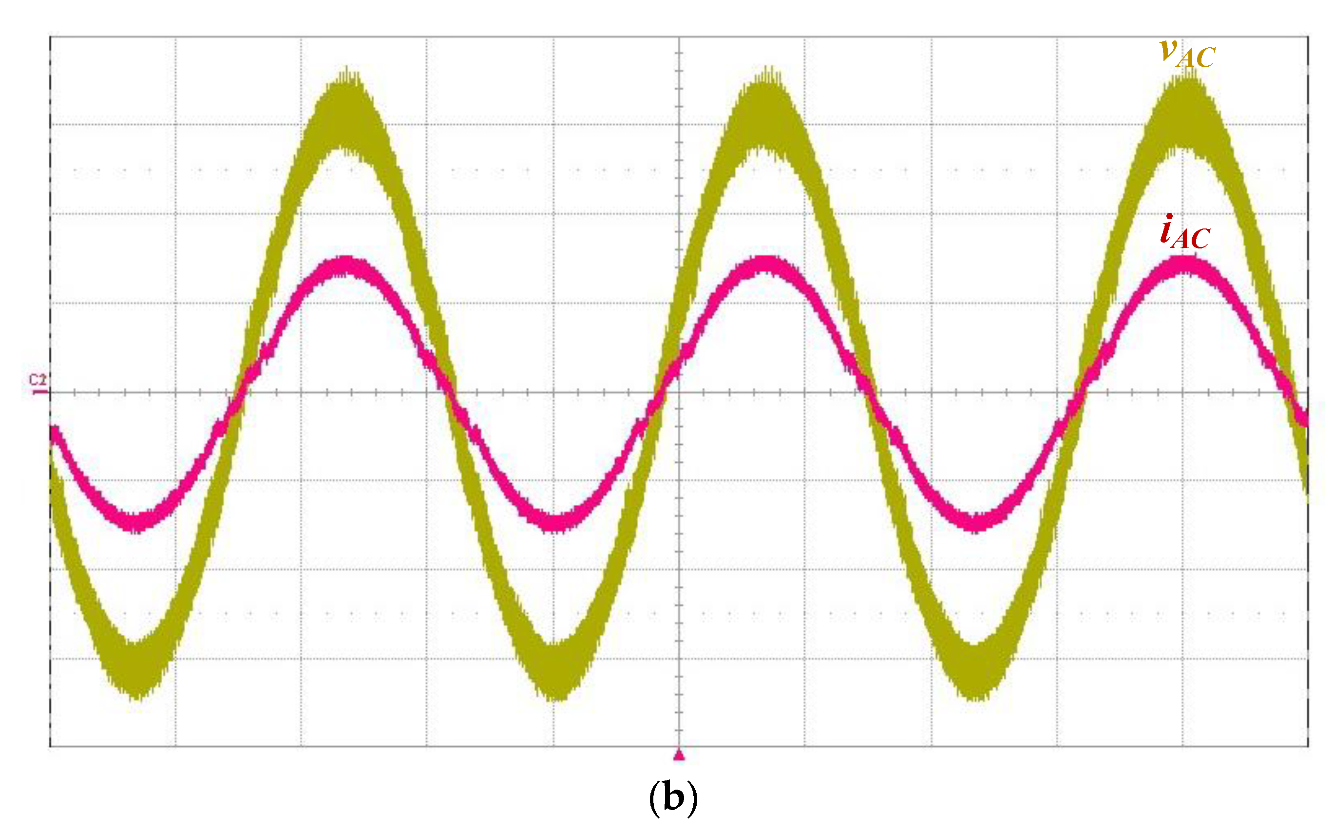
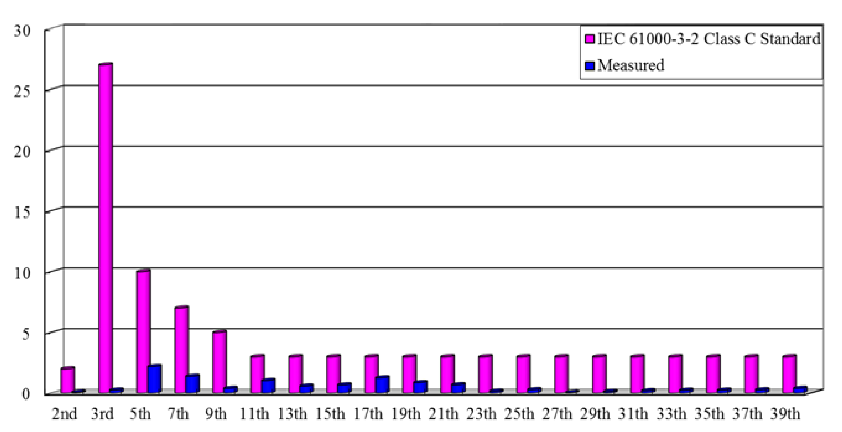
3. Experimental Results of the Proposed Drive Circuit
4. Conclusions
Author Contributions
Funding
Conflicts of Interest
References
- Lee, J.H.; Lee, H.C.; Choi, J.H.; Park, S.J.; Nam, H.G. 10kW Industrical Ultrasonic Welder Design. In Proceedings of the 31st International Telecommunications Energy Conference, Incheon, Korea, 18–22 October 2009; pp. 1–6. [Google Scholar]
- Tsujino, J.; Hongoh, M.; Yoshikuni, M.; Miura, H.; Ueoka, T. Welding Characteristics and Temperature Rises of Various Frequency Ultrasonic Plastic Welding. In Proceedings of the 2005 IEEE Ultrasonics Symposium, Rotterdam, The Netherlands, 18–21 September 2005; pp. 707–712. [Google Scholar]
- Kauczor, C.; Frohleke, N. Inverter Topologies for Ultrasonic Piezoelectric Transducers with High Mechanical Q-Factor. In Proceedings of the Annual IEEE Power Electronics Specialists Conference, Aachen, Germany, 20–25 June 2004; Volume 4, pp. 2736–2741. [Google Scholar]
- Yu, T.; Lee, H.; Lee, D.; Song, S.; Kim, D.; Park, S. Design of LC Resonant Inverter for Ultrasonic Metal Welding System. In Proceedings of the 2008 International Conference on Smart Manufacturing Application, Goyangi, Korea, 9–11 April 2008; pp. 543–548. [Google Scholar]
- Agbossou, K.; Dion, J.-L.; Carignan, S.; Abdelkrim, M.; Cheriti, A. Class D Amplifier for a Power Piezoelectric Load. In IEEE Transactions on Ultrasonics, Ferroelectrics, and Frequency Control; IEEE: Piscataway, NJ, USA, 2000; Volume 47, pp. 1036–1041. [Google Scholar]
- Ma, K.H.; Chang, W.C.; Lee, Y.C. A New Tracking Method with FPGA Chip for Ultrasonic Welding System. In Proceedings of the 2009 International Conference on Power Electronics and Drive Systems, Taipei, Taiwan, 2–5 November 2009; pp. 369–370. [Google Scholar]
- Volosencu, C. Control System for Ultrasonic Welding Devices. In Proceedings of the IEEE International Conference on Automation, Quality and Testing, Cluj-Napoca, Romania, 22–25 May 2008; Volume 2, pp. 135–140. [Google Scholar]
- Lian, Y.; Gao, C.; Liu, X. A hybrid driving strategy for piezoelectric actuator. In Proceedings of the 2013 International Conference on Mechatronic Sciences, Electric Engineering and Computer (MEC), Shenyang, China, 20–22 December 2013; pp. 3800–3804. [Google Scholar]
- Cheng, L.; Kang, Y.; Chen, C. A Resonance-Frequency-Tracing Method for a Current-Fed Piezoelectric Transducer. In IEEE Transactions on Industrial Electronics; IEEE: Piscataway, NJ, USA, 2014; Volume 61, pp. 6031–6040. [Google Scholar]
- Ghasemi, N.; Zare, F.; Davari, P.; Weber, P.; Langton, C.; Ghosh, A. Power electronic converters for high power ultrasound transducers. In Proceedings of the 2012 7th IEEE Conference on Industrial Electronics and Applications (ICIEA), Singapore, 18–20 July 2012; pp. 647–652. [Google Scholar]
- Zhou, Y.; Zhou, B.; Li, S. Driving Performance Analysis of a Novel Piezoelectric Actuator. In Proceedings of the 2010 International Conference on Measuring Technology and Mechatronics Automation, Washington, DC, USA, 13–14 March 2010; pp. 34–37. [Google Scholar]
- Lai, J.A. Two-Stage Driver for Piezoelectric Actuator. Master’s Thesis, Chung Yuan Christian University, Taoyuan City, Taiwan, 2004. Available online: https://hdl.handle.net/11296/qmkd88 (accessed on 9 October 2021).
- Jittakort, J.; Sangswang, A.; Naetiladdanon, S.; Koompai, C.; Chudjuarjeen, S. Full Bridge Resonant Inverter Using Asymmetrical Control with Resonant-frequency Tracking for Ultrasonic Cleaning Applications. J. Power Electron. 2017, 17, 1150–1159. [Google Scholar]
- Jittakort, J.; Sangswang, A.; Naetiladdanon, S.; Chudjuarjeen, S.; Koompai, C. LCCL Series Resonant Inverter for Ultrasonic Dispersion System with Resonant Frequency Tracking and Asymmetrical Voltage Cancellation Control. In Proceedings of the IECON 2015—41st Annual Conference of the IEEE Industrial Electronics Society, Yokohama, Japan, 9–12 November 2015. [Google Scholar]
- Cheng, C.A.; Chang, C.H.; Cheng, H.L.; Chung, T.Y. A single-stage high-PF driver for supplying a T8-type LED lamp. In Proceedings of the International Power Electronics Conference (IPEC-Hiroshima 2014—ECCE Asia), Hiroshima, Japan, 18–21 May 2014; pp. 2523–2528. [Google Scholar]


| Item | Conventional Two-Stage Drive Circuit [12] | Conventional Two-Stage Drive Circuit [13,14] | Proposed Single-Stage Drive Circuit |
|---|---|---|---|
| Number of Required Power Switches | 5 | 4 | 2 |
| Number of Required Diodes | 1 | 8 | 2 |
| Number of Required Capacitors | 1 | 1 | 3 |
| Number of Required Magnetic Components | 2 | 1 | 3 |
| Input Voltage Source Suitable for the Application | DC Voltage | AC Voltage | AC Voltage |
| Function of Power-Factor-Correction | Not Available | No | Yes |
| Soft-Switching of Power Switches | Not All Switches | Yes (All Switches) | Yes (All Switches) |
| Main Power Devices | Mode 1 | Mode 2 | Mode 3 | Mode 4 | Mode 5 | Mode 6 |
|---|---|---|---|---|---|---|
| Switch S1 | On | Off | Off | Off | Off | Off |
| Switch S2 | Off | Off | Off | On | Off | Off |
| Diode D1 | On | On | On | Off | Off | On |
| Diode D2 | Off | Off | Off | Off | Off | Off |
| Inductor LB1 | Charging | Discharging | Discharging | Discharging | Not Available | Charging |
| Inductor LB2 | Not Available | Not Available | Not Available | Not Available | Not Available | Not Available |
| Inductor Lr | Charging | Discharging | Discharging | Discharging | Discharging | Charging |
| Capacitor CDC1 | Discharging | Discharging | Charging | Not Available | Discharging | Charging |
| Capacitor CDC2 | Not Available | Charging | Charging | Discharging | Discharging | Not Available |
| Parameter | Value |
|---|---|
| Resonant Frequency fr | 40 kHz |
| Mechanical Equivalent Resistance Rm | 25 Ω |
| Static Capacitance Cp | 4000 pF |
| Rated Power PO | 50 W |
| Parameter/Component | Value |
|---|---|
| Diode D1, D2 | MUR460 |
| Filter Inductor Lf | 3.36 mH |
| Filter Capacitor Cf | 470 nF |
| Coupled Inductor LB1, LB2 | 500 μH |
| DC-linked Capacitor CDC1, CDC2 | 220 μF |
| Power Switches S1, S2 | W12NK90Z |
| Resonant Inductor Lr | 3.95 mH |
Publisher’s Note: MDPI stays neutral with regard to jurisdictional claims in published maps and institutional affiliations. |
© 2021 by the authors. Licensee MDPI, Basel, Switzerland. This article is an open access article distributed under the terms and conditions of the Creative Commons Attribution (CC BY) license (https://creativecommons.org/licenses/by/4.0/).
Share and Cite
Cheng, C.-A.; Cheng, H.-L.; Chang, C.-H.; Chang, E.-C.; Tsai, C.-Y.; Lan, L.-F. A Novel and Cost-Effective Drive Circuit for Supplying a Piezoelectric Ceramic Actuator with Power-Factor-Correction and Soft-Switching Features. Micromachines 2021, 12, 1229. https://doi.org/10.3390/mi12101229
Cheng C-A, Cheng H-L, Chang C-H, Chang E-C, Tsai C-Y, Lan L-F. A Novel and Cost-Effective Drive Circuit for Supplying a Piezoelectric Ceramic Actuator with Power-Factor-Correction and Soft-Switching Features. Micromachines. 2021; 12(10):1229. https://doi.org/10.3390/mi12101229
Chicago/Turabian StyleCheng, Chun-An, Hung-Liang Cheng, Chien-Hsuan Chang, En-Chih Chang, Chih-Yang Tsai, and Long-Fu Lan. 2021. "A Novel and Cost-Effective Drive Circuit for Supplying a Piezoelectric Ceramic Actuator with Power-Factor-Correction and Soft-Switching Features" Micromachines 12, no. 10: 1229. https://doi.org/10.3390/mi12101229
APA StyleCheng, C.-A., Cheng, H.-L., Chang, C.-H., Chang, E.-C., Tsai, C.-Y., & Lan, L.-F. (2021). A Novel and Cost-Effective Drive Circuit for Supplying a Piezoelectric Ceramic Actuator with Power-Factor-Correction and Soft-Switching Features. Micromachines, 12(10), 1229. https://doi.org/10.3390/mi12101229