Novel Miniature and Selective Combustion-Type CMOS Gas Sensor for Gas-Mixture Analysis—Part 1: Emphasis on Chemical Aspects


Abstract
1. Introduction
2. Materials and Methods
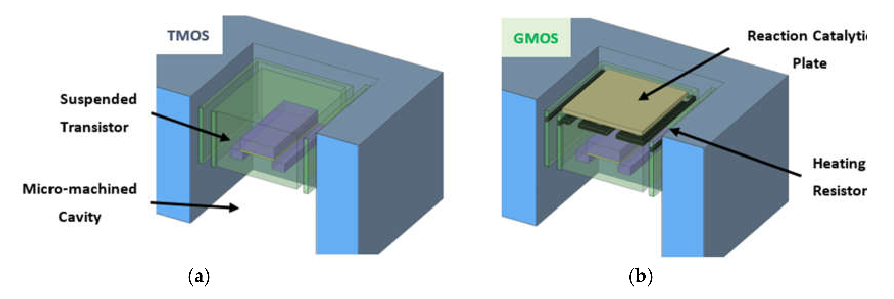
2.1. GMOS Design and Operation Principle
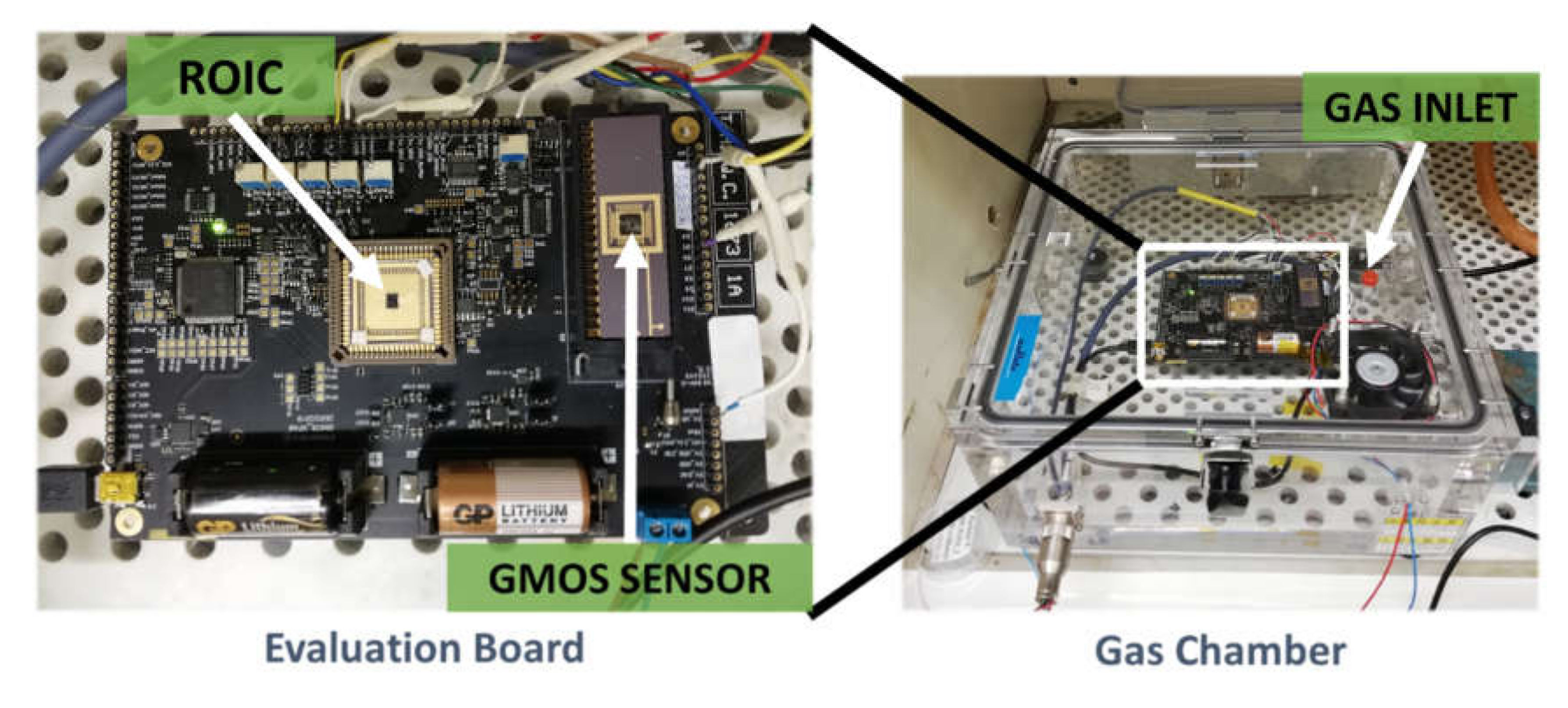
2.2. Experiment Gas Chamber
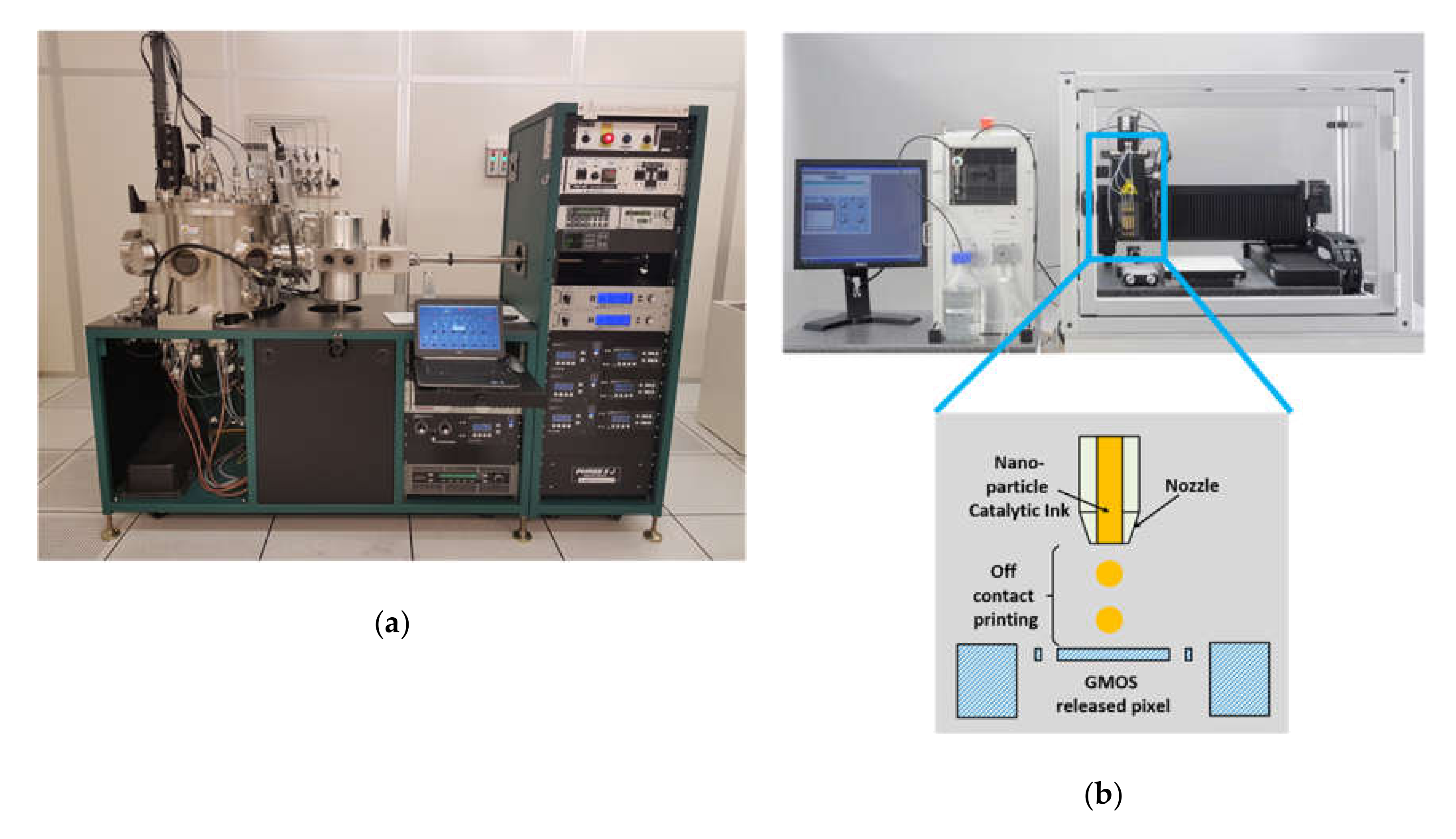
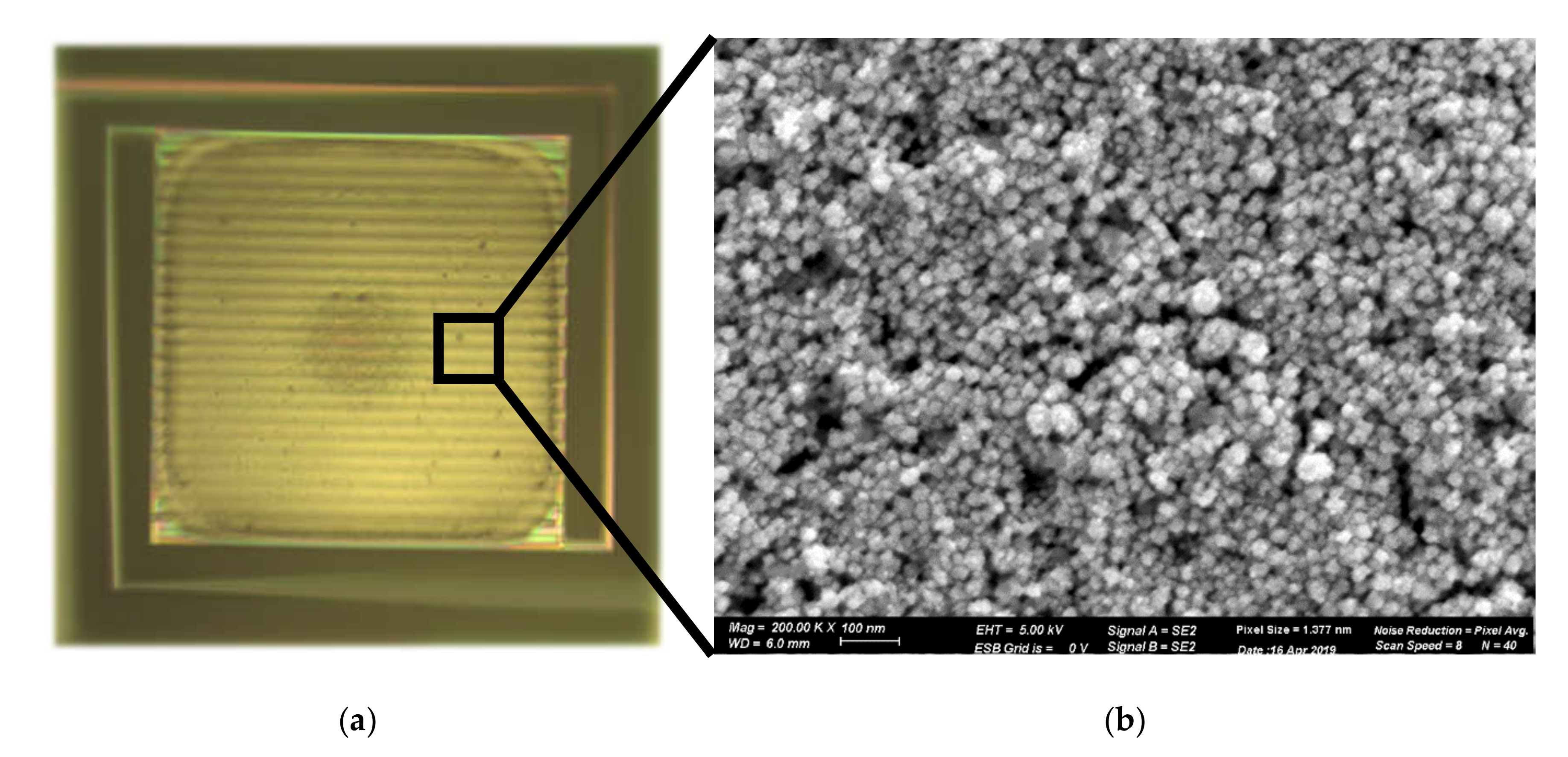
2.3. Catalyst-Deposition Technology
3. Results and Discussion
3.1. GMOS Performance Model
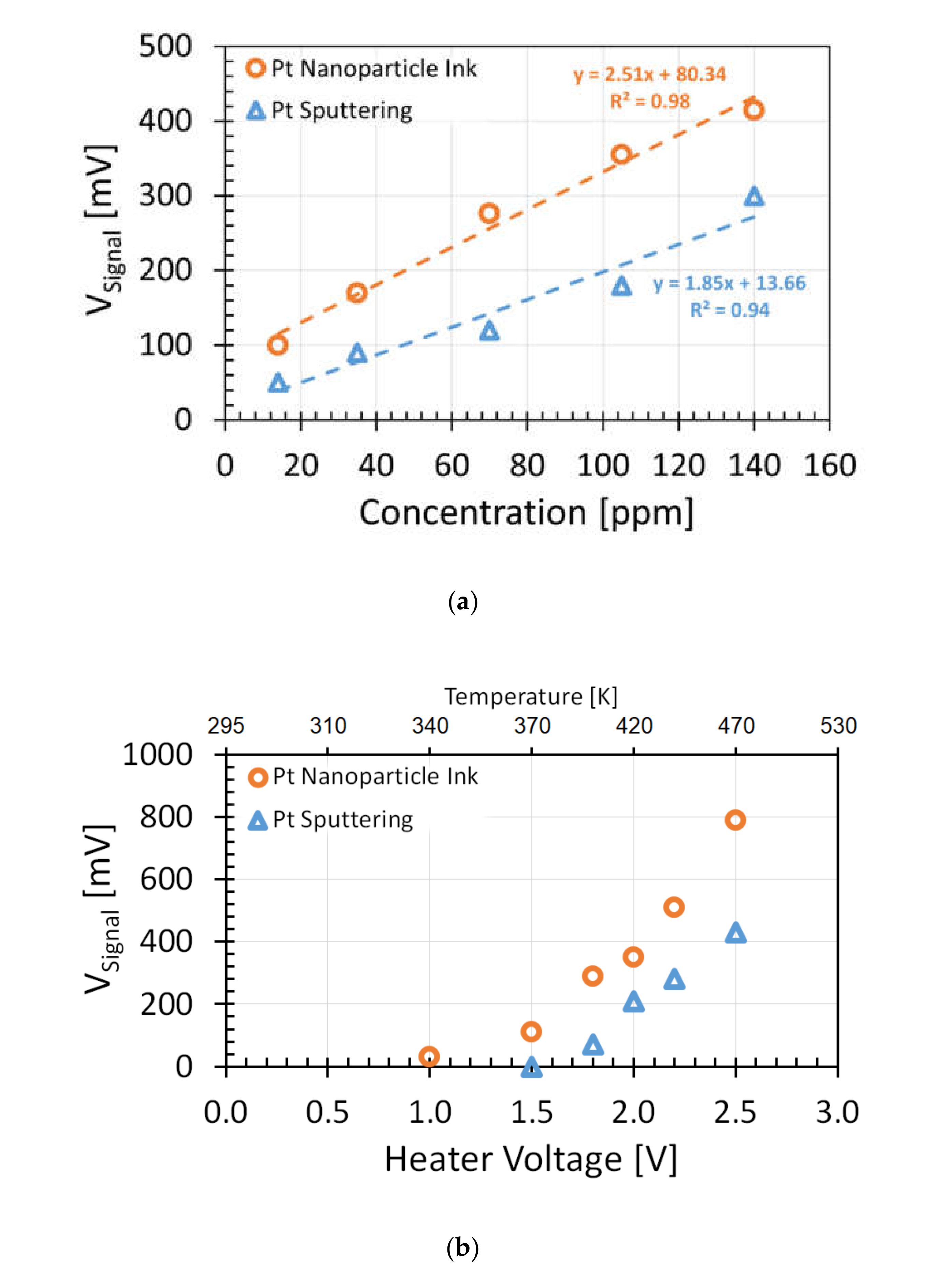
3.2. Sensitivity
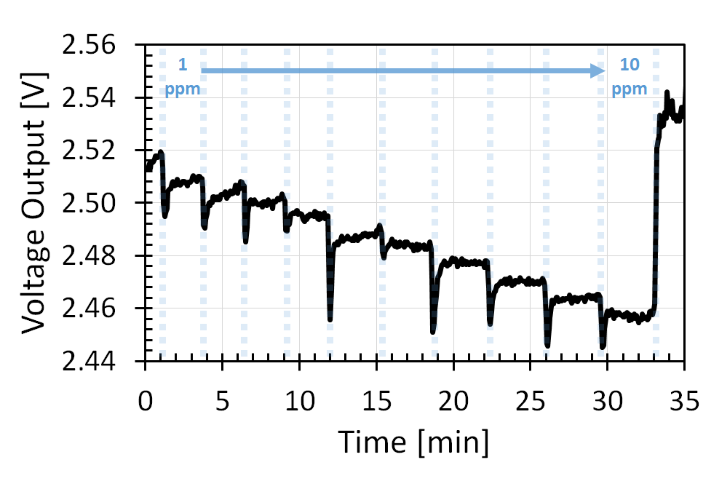
3.3. Resolution
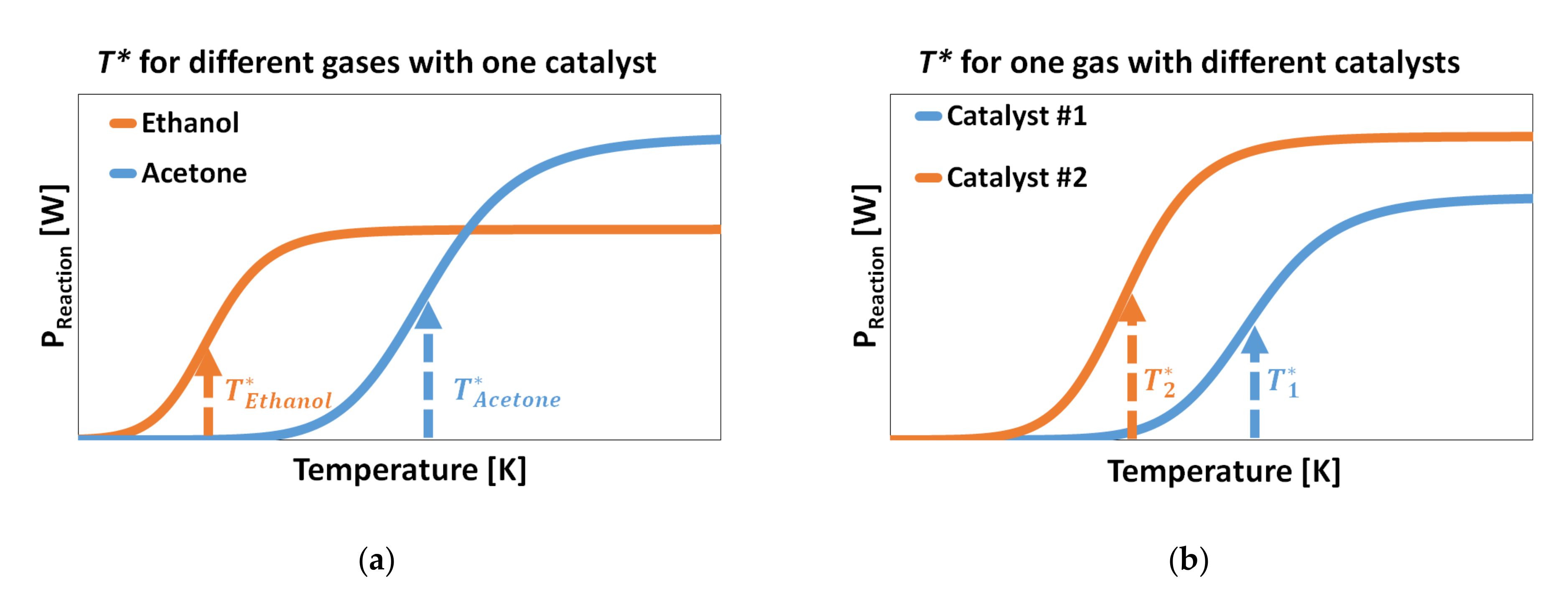
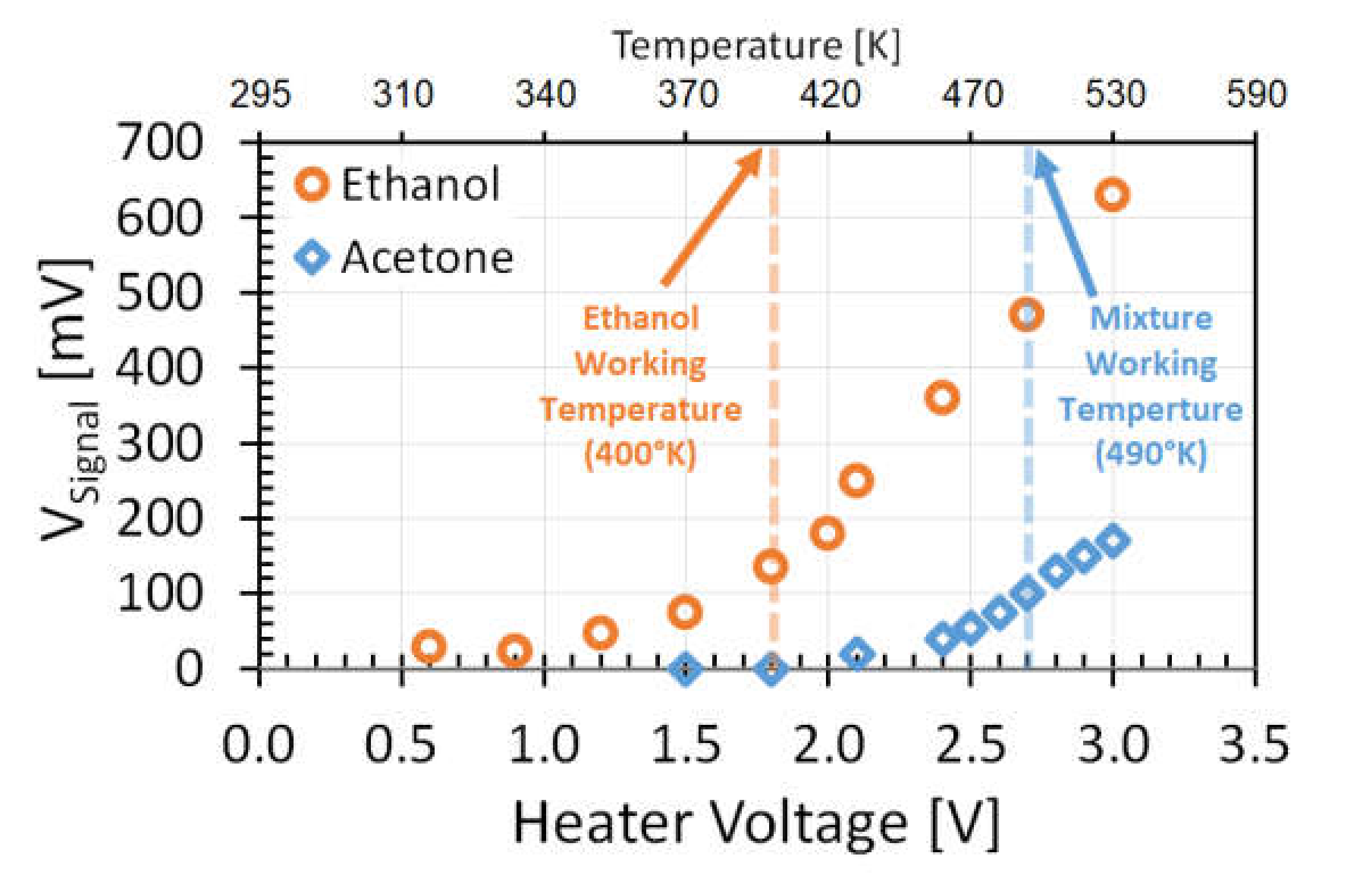
3.4. Selectivity
4. Conclusions
Author Contributions
Funding
Conflicts of Interest
References
- Fleischer, M.; Lehmann, M. Solid State Gas Sensors–Industrial Application (Springer Series on Chemical Sensors and Biosensors); Fleischer, M., Lehmann, M., Eds.; Springer: Berlin/Heidelberg, Germany, 2012; pp. 3–12. [Google Scholar] [CrossRef]
- Graf, M.; Barrettino, D.; Baltes, H.P.; Hierlemann, A. CMOS Hotplate Chemical Microsensors; Springer: Berlin/Heidelberg, Germany, 2007. [Google Scholar]
- Hierlemann, A. Integrated Chemical Microsensor Systems in CMOS Technology; Springer: Berlin/Heidelberg, Germany, 2005. [Google Scholar] [CrossRef]
- Gardner, J.W.; Guha, P.K.; Udrea, F.; Covington, J.A. CMOS interfacing for integrated gas sensors: A review. IEEE Sens. J. 2020, 10, 1833–1848. [Google Scholar] [CrossRef]
- Jaaniso, R.; Tan, O.K. Semiconductor Gas Sensors; Jaaniso, R., Tan, O.K., Eds.; Woodhead Publishing: Cambridge, UK, 2013. [Google Scholar]
- Korotcenkov, G. Handbook of Gas Sensor Materials: Properties, Advantagesand Shortcomings for Applications: Conventional Approaches; Springer: New York, NY, USA, 2013; Volume 1. [Google Scholar] [CrossRef]
- Korotcenkov, G. Handbook of Gas Sensor Materials: Properties, Advantages and Shortcomings for Applications; Springer: New York, NY, USA, 2014; Volume 2. [Google Scholar] [CrossRef]
- Ihokure, K.; Watson, J. The Stannic Oxide Gas Sensor Principles and Applications; CRC Press: Boca Raton, FL, USA, 1994. [Google Scholar] [CrossRef]
- Symons, E.A. Catalytic gas sensors. In Gas Sensors Principles, Operation and Developments, 1st ed.; Sberveglieri, G., Ed.; Springer: Dordrecht, The Netherlands, 1992; pp. 169–185. [Google Scholar]
- Miller, J.B. Catalytic sensors for monitoring explosive atmospheres. IEEE Sens. J. 2001, 1, 88–93. [Google Scholar] [CrossRef]
- Firth, J.G.; Jones, A.; Jones, T.A. The principles of the detection of flammable atmospheres by catalytic devices. Combust. Flame 1973, 20, 303–311. [Google Scholar] [CrossRef]
- Riegel, J.; Härdtl, K.H. Analysis of combustible gases in air with calorimetric gas sensors based on semiconducting BaTiO3 ceramics. Sens. Actuators B Chem. 1990, 1, 54–57. [Google Scholar] [CrossRef]
- Pranti, A.S.; Loof, D.; Kunz, S.; Zielasek, V.; Bäumer, M.; Lang, W. Ligand-linked nanoparticles-based hydrogen gas sensor with excellent homogeneous temperature field and a comparative stability evaluation of different ligand-linked catalysts. Sensors 2019, 19, 1205. [Google Scholar] [CrossRef] [PubMed]
- Brauns, E.; Morsbach, E.; Kunz, S.; Bäumer, M.; Lang, W. A fast and sensitive catalytic gas sensors for hydrogen detection based on stabilized nanoparticles as catalytic layer. Sens. Actuators B Chem. 2014, 193, 895–903. [Google Scholar] [CrossRef]
- Gitelman, L.; Stolyarova, S.; Bar-Lev, S.; Gutman, Z.; Ochana, Y.; Nemirovsky, Y. CMOS-SOI-MEMS transistor for uncooled IR imaging. IEEE Trans. Electron Devices 2009, 56, 1935–1942. [Google Scholar] [CrossRef]
- Nemirovsky, Y.; Svetlitza, A.; Brouk, I.; Stolyarova, S. Nanometric CMOS-SOI-NEMS transistor for uncooled THz sensing. IEEE Trans. Electron Devices 2013, 60, 1575–1583. [Google Scholar] [CrossRef]
- Saraf, T.; Brouk, I.; Bar-Lev, S.; Unikovsky, A.; Blank, T.; Radhakrishnan, P.; Nemirovsky, Y. CMOS-SOI-MEMS uncooled infrared security sensor with integrated readout. IEEE J. Electron Device Soc. 2016, 4, 155–162. [Google Scholar] [CrossRef]
- Zviagintsev, A.; Blank, T.; Brouk, I.; Bloom, I.; Nemirovsky, Y. Modeling the performance of nano machined CMOS transistors for uncooled IR sensing. IEEE Trans. Electron Devices 2017, 64, 4657–4663. [Google Scholar] [CrossRef]
- Zviagintsev, T.; Blank, I.; Brouk, S.; Bar-Lev, S.; Stolyarova, A.; Svetlitza, I.B.; Nemirovsky, Y. Micro-machined CMOS-SOI transistor (TMOS) thermal sensor operating in air. In Proceedings of the IEEE COMCAS—International Conference on Microwaves, Communications, Antennas and Electronic Systems, Tel Aviv, Israel, 13–15 November 2017. [Google Scholar] [CrossRef]
- Nemirovsky, Y. Gas Sensing Device and a Method for Sensing Gas. TODOS-Technion Patent. 20190011415, 10 January 2019. [Google Scholar]
- Nemirovsky, Y.; Nemirovsky, A.; Melman, S. Gas Sensing Device having Distributed Gas Sensing Elements and a Method for Sensing Gas. TODOS-Technion Patent. US20190011415A1, 1 August 2016. [Google Scholar]
- Nemirovsky, Y.; Stolyarova, S.; Blank, T.; Svetlitza, A.; Bar-Lev, S.; Zviagintsev, A.; Brouk, I. A new pellistor-like gas sensor based on micromachined CMOS transistor. IEEE Trans. Electron Devices 2018, 99, 5494–5498. [Google Scholar] [CrossRef]
- Shlenekvitch, D.; Avraham, M.; Stolyarova, S.; Blank, T.; Nemirovsky, Y. Catalytic gas sensor based on micro machined cmos transistor. In Proceedings of the 2019 IEEE International Conference on Microwaves, Antennas, Communications and Electronic Systems COMCAS, Tel Aviv, Israel, 4–6 November 2019. [Google Scholar] [CrossRef]
- Bartholomew, C.H.; Farrauto, R.J. Catalyst Deactivation: Causes, Mechanisms, and Treatment, Fundamentals of Industrial Catalytic Processes, 2nd ed.; Wiley: New Jersey, NJ, USA, 2011; pp. 260–293. [Google Scholar] [CrossRef]
- Bogue, R. Recent developments in MEMS sensors: A review of applications, markets and technologies. Sens. Rev. 2013, 33, 300–304. [Google Scholar] [CrossRef]
- SGX Sensortech. Available online: http://www.sgxsensortech.com/ (accessed on 25 March 2020).
- Magnetron Sputter Deposition System AJA International Inc. ATC 2200. Available online: http://www.ajaint.com/ (accessed on 25 March 2020).
- Scienion. Available online: https://www.scienion.com/ (accessed on 25 March 2020).
- Brauns, E.; Morsbach, E.; Schnurpfeil, G.; Bäumer, M.; Lang, W. A miniaturized catalytic gas sensor for hydrogen detection based on stabilized nanoparticles as catalytic layer. Sens. Actuators B Chem. 2013, 187, 420–425. [Google Scholar] [CrossRef]
- Fraunhofer Institute for Ceramic Technologies and Systems IKTS. Available online: https://www.ikts.fraunhofer.de/en.html (accessed on 25 March 2020).
- Frank-Kamenetskii, D.A. Diffusion and Heat Exchange in Chemical Kinetics; Princeton University Press: Princeton, NJ, USA, 1955; pp. 288–292. [Google Scholar]
- Schwartz, A.; Holbrook, L.L.; Wise, H. Catalytic oxidation studies with platinum and palladium. J. Catal. 1971, 21, 199–207. [Google Scholar] [CrossRef]


© 2020 by the authors. Licensee MDPI, Basel, Switzerland. This article is an open access article distributed under the terms and conditions of the Creative Commons Attribution (CC BY) license (http://creativecommons.org/licenses/by/4.0/).
Share and Cite
Shlenkevitch, D.; Stolyarova, S.; Blank, T.; Brouk, I.; Nemirovsky, Y. Novel Miniature and Selective Combustion-Type CMOS Gas Sensor for Gas-Mixture Analysis—Part 1: Emphasis on Chemical Aspects. Micromachines 2020, 11, 345. https://doi.org/10.3390/mi11040345
Shlenkevitch D, Stolyarova S, Blank T, Brouk I, Nemirovsky Y. Novel Miniature and Selective Combustion-Type CMOS Gas Sensor for Gas-Mixture Analysis—Part 1: Emphasis on Chemical Aspects. Micromachines. 2020; 11(4):345. https://doi.org/10.3390/mi11040345
Chicago/Turabian StyleShlenkevitch, Dima, Sara Stolyarova, Tanya Blank, Igor Brouk, and Yael Nemirovsky. 2020. "Novel Miniature and Selective Combustion-Type CMOS Gas Sensor for Gas-Mixture Analysis—Part 1: Emphasis on Chemical Aspects" Micromachines 11, no. 4: 345. https://doi.org/10.3390/mi11040345
APA StyleShlenkevitch, D., Stolyarova, S., Blank, T., Brouk, I., & Nemirovsky, Y. (2020). Novel Miniature and Selective Combustion-Type CMOS Gas Sensor for Gas-Mixture Analysis—Part 1: Emphasis on Chemical Aspects. Micromachines, 11(4), 345. https://doi.org/10.3390/mi11040345