Abstract
In the first decade of our century, carbon nanotubes (CNTs) became a wonderful emitting material for field-emission (FE) of electrons. The carbon nanotube field-emission (CNT-FE) cathodes showed the possibility of low threshold voltage, therefore low power operation, together with a long lifetime, high brightness, and coherent beams of electrons. Thanks to this, CNT-FE cathodes have come ahead of increasing demand for novel self-sustaining and miniaturized devices performing as X-ray tubes, X-ray spectrometers, and electron microscopes, which possess low weight and might work without the need of the specialized equipped room, e.g., in a harsh environment and inaccessible-so-far areas. In this review, the author discusses the current state of CNT-FE cathode research using CNT suspensions. Included in this review are the basics of cathode operation, an evaluation, and fabrication techniques. The cathodes are compared based on performance and correlated issues. The author includes the advancement in field-emission enhancement by postprocess treatments, incorporation of fillers, and the use of film coatings with lower work functions than that of CNTs. Each approach is discussed in the context of the CNT-FE cathode operating factors. Finally, we discuss the issues and perspectives of the CNT-FE cathode research and development.
1. Introduction
A focused beam of electrons is used in a wide spectrum of applications, including atomic-resolution imaging, chemical and crystallography analyses, cancer therapies, nanotechnology, and entertainment. It is implemented in electron microscopes, X-ray spectrometry, X-ray sources, and flat panel displays. Recently, there has been an increasing demand for miniaturized FE electron sources, especially for mobile devices [1,2,3,4,5] in order to extend their ability to work, e.g., in harsh and inaccessible environments. This progress might soon be expanded into novel hybrid devices, which might combine the miniaturized devices for energy harvesting, energy storage, and field emission [6]. The use of a miniaturized FE electron source could reduce the overall size of the final device. This is because FE electron sources, in contrast to thermionic electron sources, do not need a cooling unit or additional space to manage to heat to about 1000 °C.
The successful implementation of miniaturized electron sources depends on a smooth know-how transfer from a laboratory to a factory. This affects the price of the final product and the cost of the material and technology. On the other hand, commercial devices operating with the electron beam (~1950 for TEM, SEM, X-ray tubes, and many others) in most cases use tungsten as the primary building material for the electron sources, particularly for cathodes. It is extracted from commodities such as scheelite and wolframite and is harder than steel, more resistant to fracturing than diamond, and it withstands high temperatures (melting point: about 3400 °C). In a natural deposit, it is provided by China that covers about 80% of the total demand, while the remains are recycled (https://minerals.usgs.gov/minerals/pubs/commodity/tungsten/myb1-2013-tungs.pdf, accessed on 23rd January 2019). It is widely accessible for about 20 USD per unit, and it has been successfully applied in electron microscopes. In these circumstances, the lack of diversity among candidate materials limits the development of novel devices. Therefore, researchers have directed their interest toward novel and recently discovered materials with new outstanding properties, such as nanowires made of silicon carbide (SiC) [7], copper sulfide (Cu2S) [8,9], nanocarbons (carbon nanotubes (CNTs), graphene, etc.) [10,11].
Nanocarbons, in the form of highly viscous suspensions, are already present as commercial products and are being used in emerging applications that evolve into mobile and wearable electronics [12,13]. Viscous suspensions as fabrication material have opened new opportunities in terms of large-area and low-cost processability, especially in the case of complex systems. For example, industrial research has indicated that slurry screen printing is a potential technology for creating a large FE area. Therefore, after more than forty years, the FE array concept has been brought to light again [14,15], highlighted by its application for X-ray tubes [16,17] to achieve higher current densities and to avoid screening effect, which is present in case of densely grown CNT forest.
In this review, the author would like to take a closer look at FE cathodes for the electron sources based on viscous suspensions made of CNTs and review their design, technology, and performance, together with their integration into specialized instruments. The author believes the data included in this review will be useful for technologists and researchers from an interdisciplinary field who would like to widen their interest in the application of CNT suspensions to form a FE cathode, especially in terms of their miniaturization, multiplication, and arrangement, which might be extended from screen printing and contact techniques toward developing 3D printing. The review content includes basics of the FE cathodes (p. 2), with the evaluation of the cathodes (p. 3) and performance factors (p. 4), CNT as an electron-emitting material (p. 4), CNT suspension for FE cathodes (p. 5), including screen-printed CNT-FE cathodes (p. 9) and CNT-FE on the tip of a rod/wire (p. 12), methods to enhance field emission, including postprocess treatment (p. 13) and addition of fillers and coatings (p. 17), and finally, a summary (p. 19), issues, and perspectives (p. 22).
2. Basics of the FE Cathodes
In order to initiate an electron beam, an electron source is needed. In the simplest setup, an electron source is built of an opposing cathode and anode separated by a vacuum gap. Various electron sources can be used to emit electrons. In the literature, we can find electron emission sources based on thermal energy [18], field emission (FE) [19], Schottky emission [20], photoemission, and secondary emission [21]. Murphy and Good [19] identified that either one of the primary conditions (temperature or electric field strength) governs electron emission or that an intermediate region exists, where the temperature and electric field both contribute to the electron emission. In the case of thermal emission, the high temperature prevails. Typically, it is required for a cathode to be heated about 103 K [19,22]. The emission takes place over the barrier, and the emission current varies with temperature. In the case of cold field emission, high field strength dominates over temperature. Emitted electrons have energies below the Fermi level. The emission current varies with the electric field strength that determines the barrier shape. In field emission, electrons are emitted in the presence of a high electric field over 108 V/cm, at high or ultra-high vacuum (UHV; ~10−5–10−10 Torr), and through quantum tunneling at room temperature [23]. In UHV, the electrons do not collide, e.g., with the residual particles, and can travel far faster than in semiconductors, without dissipation of energy. The FE cathode, also known as a cold cathode, is used to emit electrons with high energy from keV to MeV from a solid surface. However, in Schottky’s sources, there is an ambiguous condition, i.e., the electric field is below 108 V/cm and acts together with thermal enhancement.
For an appropriate and thorough theoretical discussion, the author would like to refer to the tutorial papers on the electron sources by Jensen [21] and Forbes [24]. For field emission, usually, the Fowler–Nordheim (F–N) equation is commonly applied [19,20]. Albeit, there is still no decisive experimental evidence for the theoretical calculations [25]; the readers should consider works of Murphy and Good, or Forbes, and others who are not mentioned here, who reported the progress in correction of the F–N equation [19,25,26,27].
2.1. Evaluation
For the basic evaluation, the FE electron sources are measured in a diode configuration, i.e., cathode–anode, with a gap between them and with vacuum pressure below 10−7 Torr in a device or chamber for stable electron emission. Such a configuration is faster and more cost-efficient compared to the triode configuration, which is formed by a cathode, an extraction electrode/gate, and an anode. The triode and diode configurations both can be regarded as an electron gun [28]. The latter is used for more sophisticated assessment, e.g., if we need to steer the emission current or focus the electron beam. The measured sample is placed in the UHV chamber and heated to ~200 °C, in order to attain the required pressure and to ensure the presence of residual gases (coming from the cathode materials, e.g., not completely removed non-water solvent), and water is excluded or at least highly reduced. In such a condition, stable emission is expected, though it is not always the rule [29,30,31]. To visualize the electron emission, as an anode, the phosphor film is used deposited on a semi-transparent or transparent substrate. As a separator, it is made either a space gap, or a dielectric frame is used made of Teflon, or glass, and then placed between the cathode and the anode.
Usually, the principal characteristic is the current–voltage (I–V) graph, with the relation of the emitted current and applied voltage difference or electric field expressed in Vμm−1.
For an array of the field emitters, in most of the papers, including some recently reported [32,33], it is related to the Fowler–Nordheim law and it has a simplified form (considered as too simplified and inadequate—for more details please refer to [25]):
where J is the current density, and E is applied local electric field at the cathode surface. E is related to the macroscopic electric field with the field enhancement factor, β; ϕ is the work function of the material—an intrinsic material property defined by the energy difference between the Fermi level and the vacuum level. A and B are constants, where A = 1.54 × 10⁻⁶ AV−2 eV and B = 6.83 × 107 cm−1 V eV−3/2 [32].
J ≈ A∙E2/ϕ exp(−B∙ϕ3/2/E)
Furthermore, to determine the field-emission properties, the I–V relation is often translated to the relation of the current density and the applied electric field (JE2 vs. 1/E), so-called “F–N coordinates” [26].
The resulted F–N plot is then approximately a linear curve, which indicates only that the emission process is probably F–N tunneling [25] The field enhancement factor, β, can be estimated from the F–N plot, using the following equation [34,35]:
where s is the slope of the F–N plot. The factor β depends on the emitting material geometry, the material crystallography [36,37], and the distance between the electrodes. In case of CNT film emitters, there is an additional difference that arises due to differences in morphology, chemical state, and variations in the experimental setup [38]. As the Fowler–Nordheim theory was derived for a flat surface, it has been proposed that a correction may be needed for surfaces when applied to a single carbon nanotube or for an emitting material shape with an extremely large curvature [39,40,41].
β = B∙ϕ3/2∙s−1
The author decided to compare only I–V and lifetime characteristics of various CNT-suspension-based FE sources. The reasons are as follows: (1) The review focuses on a technological aspect of the FE sources made of CNT-based suspensions, and (2) to avoid the misjudgment, considering the wide spectrum of the F–N equations and recent progress, as it has been mentioned at the begin of this section. Especially, as in recent reported scientific discussion [25], it was proposed to use the modified F–N equations named Murphy–Good equations and the Schottky–Nordheim barrier that represent better physics to explain and interpret the FE characteristics. The Seppen–Katamuki (SK) analysis should also be recalled here, as it enables us to obtain the exact work function of the emitter, as well as to extract geometrical parameters of the field emitter [42]; for example, SK analysis has been used to evaluate the changes in work function at elevated temperature [43] or to derivate the length of carbon nanotubes in the field-emission arrays [44].
In addition to the F–N plot, the emission current stability is evaluated for its lifetime stability, often referred to as a lifetime or aging test. The aging test is considered due to a few factors. One of them is residual ionized gases present in the cathode, surrounding and coming into physical and chemical reaction with the emitting material. Another one is degradation due to resistive heating, which takes place during emission. Resistive heating promotes the thermal decomposition of the emitting material due to high emission currents. It leads to the thermal instability of the cathode [45,46]. It has an influence on the electrical and thermal conductivity of the emitting material. On the other hand, it promotes emission. Hence, there might be a transition from field emission to thermal emission.
2.2. Performance Factors
To describe field emission quantitatively, few parameters are used, such as turn-on field, TOF, threshold field, Eth, or threshold voltage, Vth, with the corresponding total current or current density [45]. These parameters can be read from I–V plots. TOF describes the required applied electric field to switch on to achieve a target emission current density; usually, it is 10 μA/cm2. A low TOF means an emitter is characterized by low applied voltages to initiate emission, low power consumption, and a long lifetime [47]. In the literature, it is also known as a turn-on electric field [12]. It should be distinguished from the “Time of Flight” (ToF) measurement used to describe the time the object (particle, wavelength, etc.) needs to travel through a defined distance in a medium. It should be separated from the threshold voltage or threshold field, which represents the tip at which measured currents exceed 0.1 pA [39].
In the literature, authors usually assign the indicated current density to the electric field or voltage applied. Therefore, this electric field and voltage were here named as the subsequent threshold electric field, Eth, or the subsequent threshold voltage, Vth, following the definition from [48].
3. CNTs as Electron-Emitting Material
To achieve the efficient FE cathode, there are two factors to be considered: the material and the cathode shape. The material should possess a low work function, to enhance electron emission. For the cathode shape, a high aspect ratio structure is a common choice, because this intensifies the electric field. In addition, from a practical standpoint, the cathode material must be compatible with current technology so that it can be shaped and arranged with the other components into an electron gun at a relatively low cost.
As mentioned in the introduction, researchers are interested in novel nanomaterials that possess outstanding properties. One such nanomaterial is the quasi-one-dimensional CNT discovered by Iijima et al. in 1991 [49]. There are numerous advantages of CNTs: (1) a high aspect ratio with a small radius curvature of the tip, which is useful to generate a high-intensity electric field to kick out the electrons; (2) high thermal end electrical conductivity; (3) mechanical strength; and (4) thermal and chemical stability [50,51]. The work function for CNT equals to 5.1 ± 0.1 eV [34]. Therefore, shortly after CNTs were discovered, they were considered to be useful as the stable FE cathodes with promising long lifetimes [52,53] that can offer high brightness, outperforming the other sources by a factor of ten [54].
CNTs were mentioned as a potential material for FE displays [55], providing a current density of a few mA/cm2 under ultra-high vacuum (~10−8 mba or 10−11 Torr) [31,56], which is close to the required level of 10–100 mA/cm2 to ensure bright electroluminescence [45]. The mechanism of electron emission from CNTs, as well as the accompanying phenomena, is described widely in [23,57,58,59,60,61] and in many other studies. With the progress in understanding further CNT-based field emission, the developments of cathodes have focused on growth techniques of CNTs in order to (1) obtain a designable device configuration on large-area substrates, (2) obtain uniform emission, (3) overcome the field screening effect [62], and, finally, (4) overcome obstacles in reducing stability of CNT-based field emission in long-term testing [63].
Work on CNT-FE cathodes started to be conducted at an industrial site by Sony, in cooperation with Candescent Technologies Corp. [64], Samsung [65,66] (Figure 1a,b), and Philips [67] (Figure 1c). The research stopped because of the emergence of the OLED; the latest news about commercial field-emission displays (FEDs) comes from 2009 [68] and 2010 [69]. Despite the stoppage, CNTs and their composites continue to be researched in terms of cold emission, which is unveiling new phenomena and mechanism models [70,71,72,73] from doped CNTs [74], CNT fibers [75,76] and rods [77], or triangular spatial film [78].
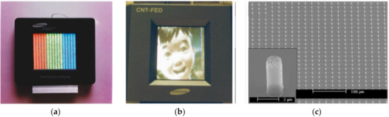
Figure 1.
Examples of the field-emission displays (FED): (a) the emitting color (red–green–blue) phosphor columns image of fully sealed SWNT-FED presented by Samsung (reprinted with permission from [65]); (b) further results from Samsung presenting the color image (reprinted with permission from [66]); and (c) a scanning electron microscopy (SEM) image of CNT arrays for the FED by Philips (reprinted with permission from [67]).
4. CNT Suspension for FE Cathodes
There are various methods for synthesizing CNTs for FE electron source cathodes, e.g., arc discharge, chemical vapor deposition (CVD), and laser vaporization [79]. The first FE cathodes were isolated multi-walled CNTs grown by a plasma arc discharging directly onto a substrate, then attached to a graphite fiber electrode [80] (Figure 2a), and followed by accurately aligned arrays of CNT forests [52,57] (Figure 2b,c). FE cathodes can be formed as well by the deposition of synthesized CNTs in electrophoresis (Figure 2d,e) [81,82]. However, each of these methods are difficult to incorporate into the technology flow of, e.g., the electron gun fabrication, because of a several reasons: (1) low-throughput [83], (2) neither the synthesized CNT forest nor deposited CNTs are fully technologically compatible with the common thin-film technology to fabricate electronics [84], and (3) the emission is affected by the screening effect between vertically standing nanotubes [85].
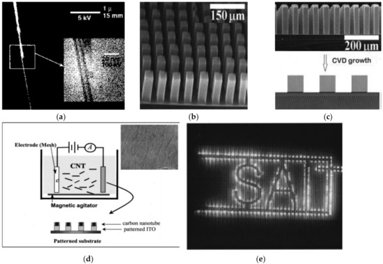
Figure 2.
First approaches toward CNT field-emission (FE) cathodes: (a) a single CNT attached to a stalk—a high-resolution SEM image and transmission electron microscope (TEM) image (inset) (reprinted with permission from [80]); (b,c) synthesized and aligned arrays of CNT forest (reprinted with permission from [52])—SEM images of CNT towers (b) and its side-view variation (c), and the schematic cross-section illustration of the array (c—lower image); (d) CNT film deposited by electrophoresis—a schematic illustration presenting the process (reprinted with permission from [82]) with an SEM image of the deposited CNT by electrophoresis (insert view) (reprinted with permission from [81]); (e) the working FED from CNTs deposited by electrophoresis (reprinted with permission from [82]).
A breakthrough to these issues was the development of an FE film cathode. It was made of dispersed CNTs in ethanol mixed into non-conducting epoxies [86]. Contrary to the vertical array, such CNT film/layer forms a mesh, i.e., randomly aligned CNTs, with a flattened surface with only a few jutting/protruding CNT tips (Figure 3a). The emission current was close to that of a single nanotube (0.1–10 μA vs. 0.1–1 μA) but at a higher bias voltage (200 V vs. 80 V) [80]. Research into this precursory film idea has been stopped for the next few years because of weak applicability, which is reflected in the lack of high brightness usually accomplished by a good electrical contact [87,88] and a high current [45]. One of the main reasons was the dependence of the emission current on the CNT density in the matrix [46]. The proof of this hypothesis was conducted by Nilsson et al. [85], who researched an FE cathode made by ink-jet printing CNT suspensions (Figure 3b,d).
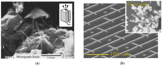
Figure 3.
The FE cathodes made of a CNT matrix: (a) an SEM image of the dispersed CNT laminated onto a 50 × 50 μm2 area, the inset—the schematic illustration presenting the CNTs matrix laminated between two glass slides (reprinted with permission from [86]); (b) an SEM image of FE cathode made by ink-jetting of dispersed CNTs—the inset presents a macroscopic emission image of 2.5 × 2.5 mm2 on the phosphor screen; (c) the illustration presenting the field screening effect issue—a simulation of the electric field penetration depth for various CNT inter-distances; (d) SEM images (left) and FE maps (right) of the FE film cathodes, relevant to simulations presented in (c)—from the top to the bottom: the FE film with the highest, medium, and the lowest density of CNTs. Figure 3b–d reprinted with permission from [85].
On the other hand, in the early stages of research on FE CNT film cathodes, the low content of CNTs in the suspensions represented a significant obstacle. Typically, these suspensions contained CNT concentrations below 0.3 wt.% and were well-suited for spraying and ink-jet printing [89,90,91,92,93]. Due to the low density of these formed films, these techniques were not extensively used for FE cathode technology [94]. Nonetheless, research into film FE cathodes has continued to reveal attractive findings: (1) CNTs can emit from sidewalls (Figure 4) [95,96], and (2) despite CNT degradation during FE, the current level for a single CNT in a film is relatively high, from 300 nA to even 10 μA per emitter. This is enough to raise the substrate temperature toward the melting point (e.g., silicon [97]). The emission current depends on the type of CNTs and the methods used to synthesize them [48]. The higher crystallinity of the CNTs resulted in less Joule heating and led to improved stability and enhanced emission current density [98], as well as in brightness homogeneity [99].
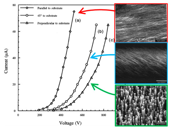
Figure 4.
Field emission from the sidewalls of CNTs: the voltage–current (I–V) characteristic of films made of CNTs aligned parallel, at 45°, and perpendicular to the substrate (reprinted with permission from [95]).
This research had an impact on the development of a uniform and large area of FE electron sources formed in a simplified process like dip-coating, drop-casting, or filtration (Figure 5a,b) [98,100,101,102,103], and finally screen printing (Figure 5c) [104,105,106], which is an established and well-known method for fine patterning, with increasing use for flexible electronics [107,108,109], including vacuum electronics [110,111]. The graph summarizing the techniques for the FE cathodes upon the alignment of the CNTs and the scalability is presented in Figure 6 (author’s work).
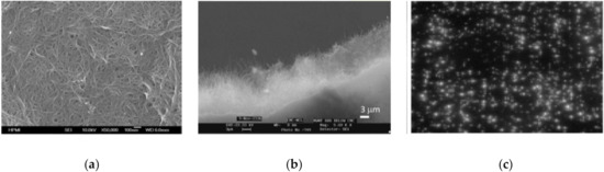
Figure 5.
Uniform and large area FE cathodes: (a,b) SEM images of the buckypaper surface reprinted with permission from [102] (a) and reprinted with permission from [103] (b); (c) the emission image of the screen-printed FED (reprinted with permission from [105]).
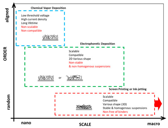
Figure 6.
The graph presenting the possible scalability (horizontal axis) and the alignment of CNTs (vertical axis) obtained for various techniques to form FE cathodes (the author’s work).
4.1. Screen-Printed CNT-FE Cathodes
Screen printing is a well-established and significantly old technique for reproducibly writing patterns on flat surfaces [112]. The print industry has been using it to transfer black-and-white and color patterns on solid and non-solid materials [113], without any limits on the patterned area. The technique uses a wire-mesh frame that is placed over a fixed substrate. The wire-mesh design and material type [114] are two important factors in considering the affinity of the wire mesh, together with the choice of the substrate and suspension (paste, ink, or emulsion) [109,114]. The important parameter in screen printing is the viscosity of the suspension, which depends on the solvent: if it is too viscous, it will not transfer through the wire-mesh opening; if it is insufficient, it will not hold the pattern [114,115]. The fabrication of the suspension is also important. Commonly used ultra-sonication or harsh mechanical crushing is well-known to damage CNTs, diminishing the suspension cohesion [115]. In addition, damage to the CNTs has shown to have a negative influence on I–V characteristics of the FE cathodes (Figure 7) [105], as well as on the resistivity of the obtained film from the suspension and threshold field (adequate voltage) at which the emission starts [55].
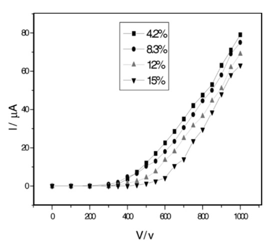
Figure 7.
The graph showing the I–V characteristic of an FE cathode made of dried CNT suspensions for different constitutes of CNTs (reprinted with permission from [105]).
The first report on screen CNT-FE cathodes came from Kwo et al. [104]. Initially, they synthesized multi-walled CNT (MWCNT) clusters by arc discharge between a pure graphite rod and a graphite disc in a helium atmosphere. They obtained micrometer-long CNT bundles and demonstrated FE condition with turn-on field (TOF) at 1.5 V/μm with an emission current density up to 7.3 mA/cm2. Next, the fibers were crushed in a ball mill for several hours, with the addition of binders (conductive pastes composed of carbonaceous particles), resulting in a CNT slurry. Finally, the slurry was screen-printed and heated (500 °C in air for 1 h), forming a CNT film. Next, its surface was etched in microwave Ar plasma for 30 s, in order to remove the binders. This improved emission characteristics (I–V). To demonstrate the potential large area patterning, the CNT cathode array was fabricated and worked as the FED (Figure 8a). The cathodes were characterized by cycling the I–V profiles, with similar emission current densities (1.5–6.5 mA/cm2) at 3 V/µm (Figure 8b) and lifetimes of about 1500 min (Figure 8b inset).
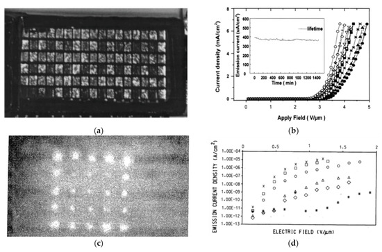
Figure 8.
One of the first screen-printed CNT-FE arrays: (a,c) images of the light emitted from various phosphors by use of the screen-printed FE cathode arrays; (b,d) FE characteristics of several screen-printed CNT films; the inset in (c)—a lifetime test showing the stability of the emission current. (a,b) reprinted with permission from [104]; (c,d) reprinted from [116].
An interesting concept to combine screen printing and lithography patterning was presented by Bouchard et al. [116]. This was one of the earliest ideas on how to make a flat panel display greater than 30 inches (76 cm) in size, with the resolution limited to single micrometers. The CNT-FE cathode was fabricated in a three-electrode setup (triode), with various components. In a sequence of patterning steps similar to thin-film technology, all of the triode setup components were screen-printed, layer by layer, as follows: a conductive path, a dielectric separator, a gate electrode, and a layer of emitting material (a cathode). Additionally, all components were screen-printed, using suspensions, to which a photosensitive agent was added. In this way, a series of various photo imageable pastes were developed that differed by composition and weight percentage (wt.%) content. A similar process used for photolithography, e.g., in semiconductor technology, was used to pattern all triode components. The screen-printed films were UV irradiated through the mask to transfer the patterns and then baked. Next, the unnecessary material was removed, leaving the patterned area. If the films, made of various pastes, were screen-printed layer by layer, then all components could be patterned at once. The technology prevented the formation of electrical shorts between electrodes and assured that the components were finely aligned and adjusted vertically. The FE cathode arrays emitting light from the phosphors are presented in Figure 8c, with the current density up to about 1 × 10⁻⁵ A/cm2 (Figure 8d).
It has been found that the design of the field emitter determines its performance. Kwon and Lee [117] showed that the peripheral length of the patterned emitters cannot be neglected as emission primarily occurred from the edges. Hence, changes in the cathode design, from the high aspect ratio lines to the matrix of squares have resulted in more uniform and 1.4 times higher emission current, probably due to the non-uniform distribution of CNT tips from the surface of the film. Further experiments by following researchers [118,119] showed an increase of emission currents with the reduction of the emitter area and the spacing between them (Figure 9a,b). All the results indicated the potential of a microscale design and the importance of the fine patterning for CNT-FE cathodes.
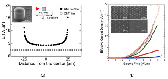
Figure 9.
Influence of a design of a cathode on its emission: (a) the graph presenting simulation results for the FE cathode being a flat film and a bundle—the trend in electric field enhancement upon the distance from the center of the cathode, and the inset shows the bundle SEM image (left) and a schematic image (right); (b) the FE characteristic of the cathodes arrays with various distances between them, and the inset shows SEM images of these FE cathodes. Figure 9a,b reprinted with permission from [118,119], respectively.
Currently, photo imageable pastes can achieve tens of micrometer resolutions of the patterns and the separation distances if used in screen printing. However, UV exposure is still limited to thin films, as the UV irradiation cannot completely penetrate thicker films to reach cross-linking agents at the bottom. Moving forward, this issue in advanced processing was presented by Chung et al. [66], and the resulting CNT FED product is presented in Figure 1b. The cathode consisted of an array of field emitting CNT with a diameter of 20 μm on indium tin oxide (ITO) (Figure 10—an upper inset). Over the tips, there was an opening window with a diameter of 30 μm in a chromium film (Figure 10 a lower inset). Both the cathode and opening were electrically isolated by silicon dioxide (SiO2) and amorphous silicon (a-Si) films. The role of the chromium film with the opening was to extract electrons that diverged radially. First, the films were deposited and patterned for conducting pads (ITO), electrical isolation (a-Si, SiO2) and photo-masking (a-Si). After that, the chromium film with the electron extraction opening was made and covered by photo imageable CNT paste. Next, the paste was UV-exposed through the transparent back-side substrate, revealing the CNT cathode film. Nonetheless, the cathode thickness was only a few micrometers (4 μm), showing that it is indeed an example of a smart technique for photopatterning thick films surrounded by other components. This is particularly important, as the usage of CNT paste usually takes place at the end of the process flow to preserve its properties. The FED worked in a triode configuration: 1.5 kV and 100 V were applied to the anode and gate, respectively. The FED achieved over 0.4 mA (see Figure 10a).
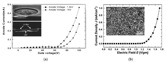
Another, but less popular, technique that was reported as using the viscous CNT suspension is electro-plating [120]. In the process, a glass substrate was dipped in a nickel sulfate bath containing CNTs, leaving on the glass surface a film with field-emission properties. After dipping for 60 s at 80 °C, the film was dried and washed in deionized (DI) water. Finally, the sample was plasma-treated to remove the organic materials present in the suspension and the plating bath. The addition of CNTs made a film with a matrix of sharp edges and tips (Figure 10b inset), which is believed to contribute to the electric field enhancement factor. However, in this case, uniformity characterization of this coating proved to be difficult, as well as making patterns on the film, as in the previous examples. The FE measurements resulted in 1 mA/cm2 at 1.7 V/μm (Figure 10b). However, during the long emission (> 20 h), the characteristics became less stable, and the TOF almost doubled. The authors related this to the degradation of the film, i.e., heat-induced fracturing. Although the morphological changes increased the film resistivity and finally increased Joule heating, the cathodes operated for about 80 h at their current density, which is a significant result for potential applications.
4.2. CNT-FE Cathodes on the Tip of a Rod/Wire
Because X-ray imaging and therapy require a highly focused beam, the CNT-FE cathodes on the tip of a rod or wire were found to be the best structure for this. At the beginning of technology for an FE cathode on a tip, either electrophoresis or direct synthesis was used to deposit CNTs on the tip [121]. A single CNT was also mounted on a tip by a specialized piezo nano-manipulator [54]. The use of printable CNT pastes for an FE cathode on a tip was first presented by Kim et al. [2], who made a sub-millimeter-wide cathode film on the tip (dia.~ 800 µm) of a W rod (Figure 11a). The cathode of such a small dimension was made by using the contact method: The rod was simply covered by a viscous CNT paste that bonded physically to the tip. The authors wanted to cover only the cross-section of the tip surface in order to get a focused beam; hence, they used only a 1 uL droplet of a prepared suspension of CNTs mixed with Ag nanoparticles. Next, the dropped suspension was dried and thermally annealed. The annealing conditions (800 °C for 2 h under vacuum) melted the Ag nanoparticles that are believed to contribute to physical bonding between the W tip and CNTs (Figure 11b inset). This kind of FE cathode achieved 10 mA/cm2 at 1.15 V/µm (Figure 11b).
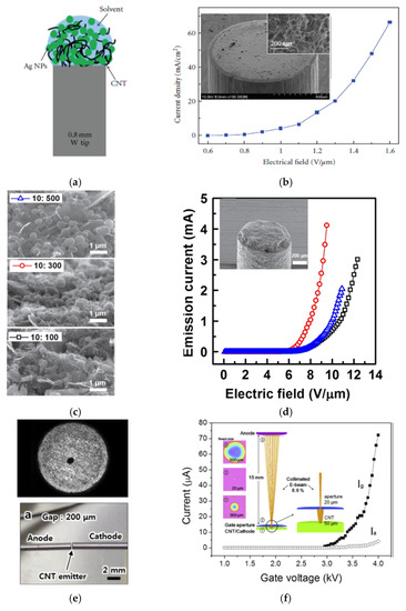
Figure 11.
The CNT-FE cathode on tip: (a) a schematic illustration of the FE cathode on a tip, using a CNT suspension with silver nanoparticles (NPs); (b,d) the FE characteristic of the cathode, the inset—a zoom on a tip with drop-casted suspension; (c) SEM images of the surface of CNT cathode on a tip with various ratios of graphite powder and CNTs; (e) an OM image of the top of CNT-FE cathode (upper view); (e) the photography of the diode configuration, including the FE cathode on a tip (lower view); (f) I–V characteristic of the CNT FED in a triode configuration, and insets shows the simulated result of a collimated electron beam. Figure 11a,b from [2], Figure 11c,d from [116], and Figure 11e,f reprinted with permission from [122].
A similar strategy was approached by Sun et al. [123]. Following the other research results, they concluded that the addition of powder graphite to a CNT paste is a better choice to enhance adhesion to the surface tip. This is due to the similar nature of the materials bonded together, i.e., graphite powder and a graphite rod. The paste was dropped on a rod tip (diameter ~700 μm) and annealed in air at least 100 °C (The authors actually performed annealing at various temperatures and duration times.), to remove residual materials. After polishing the tip in order to protrude the CNTs, the cathode was ready for testing. The cathodes were made of pastes with three various ratios of CNTs to graphite powder: 10:100, 10:300, and 10:500 (Figure 11c). As expected, the highest content of graphite powder resulted in fewer CNTs being visible on the surface of the tip (Figure 11d inset). However, surprisingly, the best FE characteristic was obtained for the cathode with a moderate ratio of CNTs (10:300) (Figure 11d). This might be explained by the diminished screening effect for a looser density of CNTs, following the conclusion raised by Nilsson et al. [85], that there exists an intermediate regime defining the optimal inter-distance between CNTs. The highest emission current was 4.1 mA and the lowest TOF was 2.8 V/µm. Additionally, the performed lifetime tests exhibited over 20 h of working, with the current declining from 1.0 to 0.6 mA.
A smaller FE cathode on the tip of a Kovar wire was reported by Choi et al. [122], and it was made by using the tip contact method. Here, CNT suspension was brought in a precisely defined contact with the polished tip surface through Ohm measurement, involving a dedicated tool. By using this method, the authors were able to make a smaller FE cathode with a diameter of 50 μm (Figure 11e—upper view). After all necessary drying, removal of organic binders, and postprocessing, the authors presented the working cathode in the diode (Figure 11e—lower view) and triode (Figure 11f inset) configuration. In such a configuration, the cathode achieved an emission current of 220 μA (11.2 A/cm2) at 3.7 kV (Figure 11f).
Further research might be provided to improve the stability and to lower TOF and threshold field at high field-emission current compared to pristine CNTs, by analogy to the reported field emitters, where CNT were grown/sprayed on or between low-melting-point (below 500 °C) metals [124], metal oxides [125], and alloys [126].
Additionally, the local deformation of the substrate should be considered. Svensson et al. [127] noticed the substrate deformation (silicon dioxide) during field emission from a single-walled CNT (SWCNT). In their experiments, they intended to grow SWCNTs by the CVD with the presence of the low electric field (10–4 Vcm−1). After the growth process, they noticed the radial deformation around the location, where SWCNT was anchored. This deformation, which is a few nm in height and a few hundred nm in width, Svensson attributed to local melting of the SiO2 in a small region underneath the SWCNTs. Because at the tip of a single CNT, a field can be on the order of V/nm, it might induce additional local field emission from the tubes. This induces Joule heating with temperatures on the order of 2000 K. Together with electron bombardment, the SiO2 substrate lower its viscosity, which causes the liquid silica to flow locally. This additionally reveals the complex nature of the field emission.
5. Methods to Enhance Field Emission
5.1. Postprocess Treatments
The FE cathode made of a viscous suspension contains randomly distributed and aligned CNTs within a medium containing additives, such as binders (Figure 12a,b). This raises the problem of electrical contact between the CNTs and the substrate [128]. Hence, to realize the optimal performance of the cathode, a post-treatment process, such as to remove additive materials and improve material cohesiveness, is needed (Figure 12c,d). This increases the emission current level and, in most cases, reduces the emission TOF. In addition, the removal of residual organic binders and additive materials diminishes the amount of outgassing of the high surface area cathode material and reduces the probability of the formation of amorphous carbon within the cathode. These aspects lead to a decrease in the overall performance of the emitter. Hence, an important issue is to remove organic additives from the dried CNT film. Most of these evaporate at a temperature above 300 °C. If the annealing is done in the air, there is a fear of burning CNTs, which can normally withstand temperatures up to 750 °C [129,130]. Hence, researchers performed a thermal process in a high vacuum, as this helps to stick to the to the temperature threshold and makes the outgassing of residual material easier [122]. A strong electric field can also be used to orient the CNTs along the field directions permanently [131], but this has not been reported for films of randomly aligned CNTs.
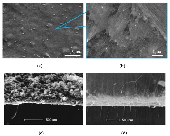
Figure 12.
CNT matrix films made of CNT suspension: (a,b) The SEM images of the CNT film made of dried suspensions, between CNTs there are visible additives in a form of balls; (c) the SEM image of CNT film with additives and (d) after they were removed; Figure 12a,b from author’s work. Figure 12c,d reprinted with permission from [132].
Zhao et al. [133] and Shin et al. [105] used the idea that specific wavelengths (266 and 349 nm) can break the chemical bonds in organic binders. As a consequence, the emission sites in the temperature threshold make the outgassing of residual material easier [122]. CNT cathodes became activated (Figure 13a,b). The authors assigned the emission improvement to photodecomposition or photo-oxidation rather than to the photothermal effect. Indeed, as irradiation intensity increased, the emission current rose from 0.0027 to 14.45 mA/cm2, while the TOF decreased from 3.7 to 1.2 V/μm (Figure 13b). A laser was also used by Rinzler et al. [80] for oxidative etching nanotubes, to open them, which contributed to field-emission enhancement. A similar approach was used by Kim et al. [134]. They developed oxidative trimming where O2 reacted selectively with the highly emitting CNTs. According to the authors, the film consisting of CNTs with uniform height ensures the spatial uniform field emission (Figure 13c,d). During the experiments, they observed gradual etching of selected CNTs. This was reflected in I–V trend lines, which exhibited the current decrease and increase with the operational time (Figure 13d inset). Despite that, during the trimming, the emission current became 80 times smaller (from 4 mA down to 0.05 mA, after the third oxidative trimming cycle), the final cathode presented a remarkably uniform emission (Figure 13d) with a stable lifetime.
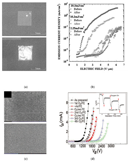
Figure 13.
Emission enhancement by a postprocess treatment: (a,c) the pair of emission patterns from CNT FE cathode arrays before (upper view), and after laser irradiation (lower view); (b,d) the FE characteristic of the cathodes before and after laser irradiation. The inset in (d) shows the cathode operation at a periodic O2 supply, i.e., oxygen trimming is on or off. Figure 13a,b reprinted with permission from [133], and Figure 13c,d reprinted with permission from [134].
Vink et al. [132], following Dupont patent [116], presented a mechanical approach to improve I–V characteristics. Cathodes were screen-printed on Al-coated glass and Au-coated Si, using a commercial screen printer, then dried (at 120 °C) and annealed (at 400 °C) for 1 h in the air. Then the adhesive tape was applied to modify the film morphology; this simple process created a sparsely distributed array of vertically oriented CNTs, which was significantly sparser than what could be grown. Meanwhile, the binders detached from the cathode surface by tensile forces and adhered to the tape (Figure 12c,d). As a result, the cathodes achieved one thousand times higher current (0.5 vs. 500 mA/cm2 at 400 V) (Figure 14a,b), close to that which was achieved by the CNT forest [52,135] or a CVD-grown CNT array net [131] (10 mA/cm2), and two orders higher than the screen-printed film cathode post-treated with Ar plasma (7 mA/cm2) [104].
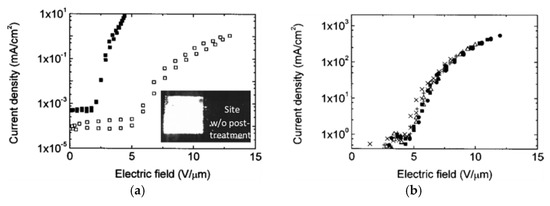
Figure 14.
Emission enhancement by a postprocess treatment: the FE characteristics of a screen-printed CNT film before (a) and after the postprocess treatment (b). The inset in (a)—the emission site density image with (left) and without (right) postprocess treatment.Figure 14a,b reprinted with permission from [132].
A similar postprocess treatment was also applied in [136,137,138,139]. However, it is difficult to discuss the effect of the treatment on emission due to a lack of data provided for comparison or other aspects influencing FE cathode properties, e.g., technology. Other methods were also investigated, such as the use of liquid elastomer [140], a soft rubber-roller [122,123,141,142,143], mechanical crush [144], and plasma [119,133,145,146,147]. The last one is believed not only to make CNTs protrude from the matrix (Figure 14c), but also to clear the cathode surface, improving the uniformity and reducing the cathode aging, and thus improving the FE characteristics (Figure 14d). In some instances, more than one technique was used [123,138,139,143]. For example, mechanical polishing and rubber rolling doubled the emission current (from 4.6 to 8.4 mA) [123]. On the other hand, the TOF increased from 2.8 to 3.2 V/µm, which the authors related to the shortened length of CNTs after the combined postprocess treatment methods.
From all reported postprocess treatment techniques, the most significant improvement was found by using poly-dimethylsiloxane elastomer (PDMS) [140]. Contrary to the other tools used in the mechanical approach, it offered several advantages: (1) It makes contact with a film surface with an inhomogeneous morphology, (2) it does not damage the CNTs, which ensures good electrical conductivity in the film, and (3) it can be applied for a complex structure containing a mask or a gate electrode, as was presented by the authors. The cathode was made from a mixture of CNTs, glass frits, and organic binders, screen-printed on an ITO glass, and dried in air (at room temperature for 10 min and at 150 °C for 1 h, and then at 300 °C.) and in a nitrogen atmosphere (at 400 °C for 30 min). Next, liquid PDMS was poured on the prepared cathode and cured at 150 °C for 10 min, to make it solid (Figure 15a). Finally, the solidified PDMS was detached from the cathode, leaving the CNT film surface with much microscale roughness (Figure 15b). The I–V characteristics improved, showing the rise of a nearly flat curve to a nonlinear shape with the emission current over 12 mA, with a uniform luminescence (Figure 15c). However, due to the lack of extensive data on optimizing the emission parameters, the possibility for significant improvement remains.
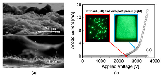
Figure 15.
Emission enhancement by a postprocess treatment: (a) SEM images of the printed CNT films before (upper view) and after (lower view) postprocess treatment; (b) I–V characteristic of the cathode before and after postprocess treatment with the inset, showing emission images of the relevant cathodes reprinted with permission from [140].
5.2. Fillers and Coatings
A filler might be understood as any type of material, other than the CNTs, that is not a solvent and has an insulating or conducting feature. The filler is added to a suspension during its preparation or postprocessing and forms solidified additives that can be geometrically defined. Common fillers are particles of nanometer or micrometer size (micro- or nano-particles), which benefit from a lower melting temperature (hundreds of °C) than their bulk form [148]. Fillers can be non-organic and organic, e.g., conductive pastes, glass frits, and metallic and polymer particles, as well as their composites and additives characterized by UV exposure sensitivity for fine patterning [105,149]. Fillers are added to the low content of CNTs in suspension, in order to serve as a bonding material for strengthening the film [150]. For example, fillers help to prevent field-dependent degradation, when the loosely bonded CNTs are extracted from the cathode by electrostatic force [97]. Fillers, then prevalent as binders, fill the empty spaces between the CNTs and the CNTs and the substrate. This improves the adhesion [2,123] necessary to perform mechanical post-treatment, ensures the recovery of the connection of CNTs which broke down due to Joule heating [72], but also enables us to avoid the arcing during emission [151]. It improves the field enhancement effects as a consequence of the protruding CNTs [139] or thermal stability, where fillers may play the role of oxidation-inhibiting compounds similar to the boron- or phosphorous-related compounds, as it has been presented by Floweri et al. [74], where the addition of Ni prevailed the degradation of the field emission.
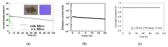
The right choice of fillers and their ratio content have shown to prolong the lifetime of the cathode by as high as 10 times [143] (Figure 16a), which, in the case of carbonaceous particles, is up to 20 h [123] (Figure 16b), while for metallic particles added to the suspension, it is up to 100 h [143] (Figure 16a,c). The ratio balance can also improve the electrical conductivity of the film [139]. Thus far, film cathodes without fillers enable current densities of tens of μA/cm2, which results in up to 1 μA (the author of the reference paper calculated the effective current density based on works of [118] and assuming that the area included in calculation is an effective emission area.), and, in some cases, to 1 mA (as previous notes.). Such a level is sufficient for the purpose of a FED source. However, for some applications, such as micro-thrusters in spacecraft or microwave amplifiers, the required current density is 100 μA/cm2 or more [152]. Cui et al. demonstrated the successful use of metal nanoparticle fillers to the cathode material [153]. In this way, they achieved emission levels at about 33.9 mA, with an emission current density of 4.2 A/cm2 from a 0.8 mm2 area of the film cathode. Despite significant progress in the technology of FE cathodes since this report, this level of performance remains exceptional.
There are also unexpected trends in the research provided toward knowing how the fillers and their ratio influence the performance of CNT film cathodes. Shin et al. [139], by changing the ratio of binders (glass frit vs. Ag paste) showed that the CNT film cathode with the highest resistance resulted in the highest current density, following the highest field enhancement factor for this sample. The authors claimed that this was due to the processing, as Ag paste served as a catalyst for the oxidation of the CNTs during the heat treatment (at 390 °C in the air). Hence, for the sample with the higher weight ratio of Ag paste, more CNTs were damaged by oxidation, which was visible by the lower number of protruded CNTs over the cathode film surface. Sun [123] showed that a high content of fillers might result in fewer emission sites. On the other hand, a lower content of fillers decreased the emission current as a consequence of the screening effect caused by higher CNT density.
One of the recent approaches to improve the field-emission performance is coating the CNT film with a low work-function material, to form a composite cathode. The approach is based on earlier findings, whereas grown-in-CVD-process CNTs were coated with lower work-function metal nanoparticles, such as Cs [154], Ti [155], Ag [156], Al [157], In [158], or Ta [159], and metal oxides, e.g., titanium oxide (TiO2) [160], and resulted in lower turn-on electric field, and threshold electric field could be achieved. In the case of a dielectric addition to the CNT array, the threshold electric field might be lower about a few times. Due to the presence of high dielectric constant material, the screening effect between CNTs is reduced, together with the mechanical stress that was generated by Joule heating. However, the work function was reported to be about half of the CNT [98,161].
The relevant work to the FE films made of CNT suspension comes from Wu et al. [35] and Song et al. [162]. The first group formed screen-printed carbon nanotubes (CNTs) and coated it with TiO2. The Ni-F was chosen as a substrate (Figure 17a) because of good electrical and thermal conductivities, whereas three-dimensional (3D) structure possessing high porosity and specific surface area enhances mechanical adhesion between the CNTs film and substrates. Finally, it can be easily and commercially obtained. The TiO2 in a form of the gel was spin-coated on the CNT film and tested. The results showed a significant reduction of the turn-on electric field and threshold voltage after coating with TiO2: from 0.75 and 1.75 V/μm to 0.40 and 0.75 V/μm, respectively (Figure 17b). The cathode operated without noticeable degradation for about 5 h. Moreover, the substrate, because of its morphology, allows for the increasing of FE sites by spreading the CNTs and, in consequence, the current density.
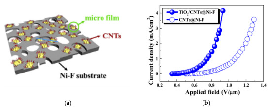
Figure 17.
The field-emission enhancement by use of film coating with the material different from CNTs: (a) a schematic illustration of CNT FE cathode on Ni–Fe foam coated with TiO2 film and (b) its FE characteristics with and without TiO2 film. Reprinted with permission from [35].
The second group chose LiF/Al (ϕ ~ 3.0 eV) to deposit on the CNT film due to the material’s low work function, equal to about 3.0 eV, and its usefulness as an efficient electron extraction layer in organic light-emitting diodes and organic solar cells [162]. In addition to the previous work, the authors precisely defined the thickness of LiF to be constant and equal to 5 nm, while the Al film to be 1 or 3 nm thick (Figure 17c). Both films were thermally evaporated on the already screen-printed CNT film. In addition to the above conditions, there was also a sample without Al coating. Next, they evaluated their relation to the field-emission properties. The authors found that the increase of the Al film thickness from 1 to 3 nm actually decreased the field-emission properties and resulted in bare improvement, considering the lifetime tests. Further research here is needed to get more data to define the right trend and confirm what the authors of the referred paper claimed, that the field-emission results are correlated with the conductivity of the composite film.
6. Summary
This paper presents field-emission-electron sources that use carbon nanotubes as the electron-emitting material. Approaches to form the FE cathode of the electron source from CNT suspensions were described and compared, including synthesis, electrophoresis, and screen printing. From all of these techniques, so far only screen printing offers a simple and scalable approach to fabricate large area and uniform for emission cathodes or cathode arrays, including their different arrangements and shapes. Meanwhile, the development of modified techniques, e.g., a combination of screen printing and photolithography, the resolution of a patterned single line can achieve even tens of micrometers. It has been shown that a suspension was successfully used for a cathode on the tip of a wire or a rod to get a highly focused electron beam. Additionally, it has been found that CNTs could emit from their sidewalls too. In many cases, various postprocess treatment methods or the addition of fillers to the suspension level up the CNTs, which indeed improves field emission and the lifetime of the cathode compared to the as-made mesh cathode. Though the overall performance of the FE cathodes fabricated from CNT suspensions is slightly inferior to that of synthesized CNTs (see the following table), from this review and other referenced works, postprocess treatments and the addition of fillers are viable approaches to improve the emission characteristics of these cathodes. As Kim [134] reported, theoretically, only a 10% difference in height of CNT tips leads to an almost 90% difference in emission currents. Thus, the precise control of the emitter array is essential to provide spatial emission uniformity. It is possible to assess the uniformity by the postprocess treatment. Therefore, it is important to adjust the parameters of post-treatment, such as process duration. For example, etching might result in over-etching of CNTs.
Table 1 and Table 2 summarize the selected cathodes mentioned in this review. Table 1 includes FE cathodes in the form of a film made of the suspension grouped by the technology used to make the cathode. Table 2 includes the cathodes made of pristine CNTs grown directly on the substrate by CVD-based methods and grouped by the structure of the cathode. The tables include the materials used for cathodes, technologies, the performance of the cathodes, and adequate references. For the performance, the best values were chosen, particularly a subsequent threshold electric field, Eth, or voltage, Vth, required for the particular emission current or current density, and duration of emission following the lifetime test. As can be seen from the wide spectrum of referenced works, the screen printing is, so far, the efficient and alternative technique to the CVD and perhaps the best solution for the large-area fabrication of the FE arrays. Additionally, the increased interest in this technique pushes forward dynamic development in viscous suspensions containing novel materials.

Table 1.
The summary of the FE cathodes in a form of a film made of the suspension, grouped according the method to form a film.
Table 2.
The summary of the remain FE cathodes, grouped according to the structure.
7. Issues and Perspectives
7.1. Field-Emission Theoretical Model
Though in the literature, for film cathodes, there is a developed theoretical model which might explain to some degree the evolution and self-assembly of the system of CNTs during field emission [158], the readers should also note the ongoing scientific discourse on the right theoretical model that describes the field emission; the commonly used Fowler–Nordheim equations were found to be inadequate and need to be corrected. So far, it is proposed to use the corrected F–N equation named Murphy–Good equations [19] in order to prevent the research-integrity problem, as it was called by R. Forbes in his latest paper [25]. Additionally, the Seppen–Katamuki (SK) analysis might be used to obtain the exact work function of the emitter, as well as to extract geometrical parameters of the field emitter [42,43,44].
7.2. Screen Printing
The major obstacle of screen printing and viscous suspensions as material for technology is the outgassing caused by the paste components during operation under vacuum conditions. In addition, the rheology of the suspension to more properly characterize the suspension is also needed to identify the critical properties, e.g., viscosity, viscoplasticity, homogeneity, etc., that determine the structure of the desired printed pattern. Another important point is that not all CNTs are the same. For example, the electronic properties of CNTs have a strong relationship with their structure, and so far it is a challenge to grow CNTs with unique electronic properties on an out-of-laboratory scale [81], making it difficult to repeat their field-emission performance. Therefore, it is important to consider that cathode performance and their processability depend on the type of CNTs used [70], as well as on their crystallinity. It was reported that high crystallinity reduced Joule heating, improved emission stability, and enhanced emission current [94] and brightness homogeneity [99]. If the FE cathode is made of CNT suspensions, its performance depends not only on the used CNTs but also on the type of solvents (organic, resins, and acids) and additives (surfactant, organic, and non-organic nanoparticles), as well as the process condition and postprocess treatment needed either to remove the solvent and additives or to protrude or rearrange the CNTs.
Finally, homogenous dispersion of the high crystalline metallic CNTs with minimal damage for field-emission purposes is not a trivial task. This point ensures the CNT cathode film stability during emission [30].
7.3. Screening Effect and Side-Wall Emission
With recent data about sidewall electron emission, flat CNT cathodes might bring some advantages, although this needs to be confirmed. Contrary to field emission from a CNT forest, in field emission from a flat CNT cathode, electric field screening phenomena seems to not play a major role. However, this issue has been not yet been investigated for the CNT matrix.
7.4. Electron Beam Focusing
Experimental data have already shown that, in the case of X-ray tubes, the sharp and irregular shape of the cathode surface causes problems with focusing the beam. An improvement was established by using a flat cathode, consisting of a CNT mesh or matrix [10]. On the other hand, the same group showed how the side-attached CNTs work as an emitter, which has a bad effect on the focusing of the electron beam, again providing an argument for planar cathodes.
7.5. Film Adhesion and Stability
Another issue related to the film cathodes is their self-assembly during emission caused by electrodynamic force and experimentally presented for CVD-grown CNTs [167]. Moreover, it will be good to investigate the influence of the adhesive layer on the field-emission properties of the CNT film, as it is suggested by Lim et al. [124], especially because there is already evidence that the weak adhesion between CNT and substrate might lead to emission instability and lowering the overall emission performance [168,169].
7.6. Addition of Fillers and Coating
Experimental proof prevailed that the presence of the intercalated metallic particles might enhance and reduce the field-emission parameters, depending on their ratio and type of the particles used [139]. The interesting comparison is between the works with attempts: (1) to make CNT film cathode free of organic or dielectric particles, and, in case of aligned CNT arrays, (2) to percolate the CNT aligned array with a dielectric material, which might have a significant impact on field-emission enhancement, and coating the cathode with a metallic film possessing lower work function than CNT showed it might be the right trend to improve the field-emission properties of the CNT film cathodes [170]. Although it had an effect on the decrease of the threshold voltage, the drawback of this approach is even three orders lower current density compared to the film cathodes without metal covering (see, for example, Figure 17 vs. Figure 4, Figure 9 and Figure 13). The influence of the coating film thickness on field-emission properties, as well as its correlation to the composite conductivity, should be further investigated to confirm the line trends and its correlation with the composite conductivity. It might also contribute to a better understanding.
All of these listed challenges should be again considered in order to have a better understanding of the electron emission from film cathodes made of CNT suspensions.
Funding
This research was financed by the National Science Centre Poland (project no. UMO-2016/21/B/ST7/02216) and statutory funds of the Wroclaw University of Science and Technology.
Acknowledgments
The author would like to thank Don N. Futaba from the National Institute of Advanced Industrial Science and Technology and Professor Anna Gorecka-Drzazga from the Wroclaw University of Science and Technology for their time to spent reviewing this paper and their valuable advice and notes.
Conflicts of Interest
The author declares no conflicts of interest.
References
- Kim, J.W.; Jeong, J.W.; Kang, J.T.; Choi, S.; Park, S.; Shin, M.S.; Ahn, S.; Song, Y.H. Great improvement in adhesion and uniformity of carbon nanotube field emitters through reactive nanometer-scale SiC fillers. Carbon 2015, 82, 245–253. [Google Scholar] [CrossRef]
- Kim, H.J.; Ha, J.M.; Heo, S.H.; Cho, S.O. Small-Sized Flat-Tip CNT Emitters for Miniaturized X-Ray Tubes. J. Nanomater. 2012, 2012, 1–6. [Google Scholar] [CrossRef]
- Basu, A.; Swanwick, M.E.; Fomani, A.A.; Velásquez-García, L.F. A portable x-ray source with a nanostructured Ptcoated silicon field emission cathode for absorption imaging of low-Z materials. J. Phys. D Appl. Phys. 2015, 48, 225501. [Google Scholar] [CrossRef]
- Evans-Nguyen, T.; Parker, C.B.; Hammock, C.; Monica, A.H.; Adams, E.; Becker, L.; Glass, J.T.; Cotter, R.J. Carbon Nanotube Electron Ionization Source for Portable Mass Spectrometry. Anal. Chem. 2011, 83, 6527–6531. [Google Scholar] [CrossRef] [PubMed]
- Krysztof, M.; Grzebyk, T.; Szyszka, P.; Laszczyk, K.U.; Gorecka-Drzazga, A.; Dziuban, J. Technology and parameters of mebrane- anode for MEMS transmission electron microscope. J. Vac. Sci. Technol. B 2018, 36, 02C107. [Google Scholar] [CrossRef]
- Chen, J.; Yang, B.; Su, D.L.; Yang, J.; Guo, R.; Tay, B.K.; Yan, X. Field emission cathode based on three-dimensional framework carbon and its operation under the driving of a triboelectric nanogenerator. Nano Energy 2018, 49, 308–315. [Google Scholar] [CrossRef]
- Chen, J.; Deng, S.Z.; Xu, N.S.; Wang, S.; Wen, X.; Yang, S.; Yang, C.; Wang, J.; Ge, W. Field emission from crystalline copper sulphide nanowire arrays. Appl. Phys. Lett. 2002, 80, 3620–3622. [Google Scholar] [CrossRef]
- Chang, T.H.; Panda, K.; Panigrahi, B.K.; Lou, S.C.; Chen, C.; Chan, H.C.; Lin, I.N.; Tai, N.H. Electrophoresis of Nanodiamond on the Growth of Ultrananocrystalline Diamond Films on Silicon Nanowires and the Enhancement of the Electron Field Emission Properties. J. Phys. Chem. C 2012, 116, 19867–19876. [Google Scholar] [CrossRef]
- Chen, L.; Yua, H.; Zhonga, J.; Wu, J.; Su, W. Graphene based hybrid/composite for electronfield emission: A review. J. Alloys Compd. 2018, 749, 60–84. [Google Scholar] [CrossRef]
- Shao, X.; Srinivasan, A.; Ang, W.K.; Khursheed, A. A high-brightness large-diameter graphene coated point cathode field emission electron source. Nat. Commun. 2018, 9, 1–8. [Google Scholar] [CrossRef]
- Gao, W.; Emaminejad, S.; Nyein, H.Y.Y.; Challa, S.; Chen, K.; Peck, A.; Fahad, H.M.; Ota, H.; Shiraki, H.; Kiriya, D.; et al. Fully integrated wearable sensor arrays for multiplexed in situ perspiration analysis. Nature 2016, 529, 509–514. [Google Scholar] [CrossRef] [PubMed]
- Huang, H.W.Y.; Xu, F.; Duan, Y.; Yin, Z. Energy Harvesters for Wearable and Stretchable Electronics: From Flexibility to Stretchability. Adv. Mater. 2016, 28, 9881–9919. [Google Scholar]
- Spindt, C.A. A Thin-Film Field-Emission Cathode. J. Appl. Phys. 1968, 39, 3504–3505. [Google Scholar] [CrossRef]
- Takao, U. Vacuum Microelectronics: What’s new and exciting. IEEE Trans. Electron Devices 1991, 38, 2276–2283. [Google Scholar]
- Schwoebel, P.R.; Brodie, I. Surface-science aspects of vacuum microelectronics. J. Vac. Sci. Technol. B 1995, 13, 1391–1410. [Google Scholar] [CrossRef]
- Chen, C.; Shao, W.; Ding, M.; Li, X.; Bai, G.; Zhang, F.; Feng, J. Development of micro-patterned carbon nanotube field emission arrays for high current applications. In Proceedings of the 2007 IEEE International Vacuum Electronics Conference, Kitakyushu, Japan, 15–17 May 2007. [Google Scholar]
- Li, X.; Bai, G.; Kou, J.; Li, H.; Hu, Y.; Cai, J.; Ding, M.; Feng, J.; Liao, F. Title of the conference paper. In Proceedings of the 2016 IEEE International Vacuum Electronics Conference, Monterey, CA, USA, 19–24 April 2016. [Google Scholar]
- Trucchi, D.M.; Melosh, N.A. Electron-emission materials: Advances, applications, and models. MRS Bull. 2017, 42, 488–492. [Google Scholar] [CrossRef]
- Murphy, E.L.; Good, R.H., Jr. Thermionic emission, field emission, and the transition region. Phys. Rev. 1956, 102, 1464–1473. [Google Scholar] [CrossRef]
- Fowler, R.H.; Nordheim, L. Electron emission in intense electric fields. Proc. R. Soc. Lond. A 1928, 119, 173–181. [Google Scholar]
- Jensen, K.L. A Tutorial on Electron Source. IEEE Trans. Plasma Sci. 2018, 46, 1881–1898. [Google Scholar] [CrossRef]
- Haase, J.R.; Go, D.B. Analysis of thermionic and thermo-field emission in microscale gas discharges. J. Phys. D Appl. Phys. 2016, 49, 1–9. [Google Scholar] [CrossRef]
- Saito, Y.; Uemura, S. Field emission from carbon nanotubes and its application to elecron sources. Carbon 2000, 38, 169–182. [Google Scholar] [CrossRef]
- Forbes, R.G. Field electron emission theory (October 2016). In Proceedings of the 2016 Young Researchers in Vacuum Micro/Nano Electronics (VMNE-YR), St. Petersburg, Russia, 5–6 October 2016. [Google Scholar]
- Forbes, R.G. Comments on the continuing widespread and unnecessary use of a defective emission equation in field emission related literature. J. App. Phys. 2019, 126, 1–14. [Google Scholar] [CrossRef]
- Forbes, R.G.; Fischer, A.; Mousa, M.S. Improved approach to Fowler–Nordheim plot analysis. J. Vac. Sci. B 2013, 31, 1–8. [Google Scholar] [CrossRef]
- Forbes, R.G. Extraction of emission parameters for large-area field emitters, using a technically complete Fowler–Nordheim type equation. Nanotechnology 2012, 23, 1–12. [Google Scholar] [CrossRef] [PubMed]
- Crewe, A.V. Electron Gun Using a Field Emission Source. Rev. Sci. Instrum. 1967, 39, 576–583. [Google Scholar] [CrossRef]
- Qian, L.; Wang, Y.Q.; Liu, L.; Fan, S.S. Nanoscale field emission in inert gas under atmospheric pressure. J. Vac. Sci. Technol. B 2010, 28, 562–566. [Google Scholar] [CrossRef]
- Shimoi, N.; Tohji, K. Current-Fluctuation Mechanism of Field Emitters Using Metallic Single-Walled Carbon Nanotubes with High Crystallinity. Appl. Sci. 2017, 7, 1322. [Google Scholar] [CrossRef]
- Tripathi, P.; Gupta, B.P.; Bhatnagar, A.; Patel, C.R.P.; Banker, P.K.; Late, D.J.; More, M.A.; Lalla, N.P.; Phase, D.M.; Choudhary, R.J.; et al. Highly efficient field emission properties of radially aligned carbon nanotubes. J. Mater. Chem. C 2018, 24, 6584–6590. [Google Scholar] [CrossRef]
- Giubileo, F.; Bartolomeo, A.D.; Iemmo, L.; Luongo, G.; Urban, F. Field Emission from Carbon Nanostructures. Appl. Sci. 2018, 8, 526. [Google Scholar] [CrossRef]
- Back, T.C.; Gruen, G.; Park, J.; Murray, P.T.; Ludwick, J.; Cahay, M.; Fairchild, S.B. Electron emission characteristics of wet spun carbon nanotube fibers. AIP Adv. 2019, 9, 065319. [Google Scholar] [CrossRef]
- de Jonge, N.; Allioux, M.; Doytcheva, M.; Kaiser, M.; Teo, K.B.K.; Lacerda, R.G.; Milne, W.I. Characterization of the field emission properties of individual thin carbon nanotubes. Appl. Phys. Lett. 2004, 85, 1607–1609. [Google Scholar] [CrossRef]
- Wu, Y.; Li, J.; Ye, J.; Song, Y.; Chen, X.; Hunag, S.; Sun, Z.; Ou-Yang, W. Outstanding field emission properties of titanium dioxide/carbon nanotube composite cathodes on 3D nickel foam. J. Alloy Compd. 2017, 726, 675–679. [Google Scholar] [CrossRef]
- Gadzuk, J.W.; Plummer, E.W. Field Emission Energy Distribution (FEED). Rev. Mod. Phys. 1973, 45, 487–548. [Google Scholar] [CrossRef]
- Michaelson, H.B. The work function of the elements and its periodicity. J. Appl. Phys. 1977, 48, 4729–4733. [Google Scholar] [CrossRef]
- Bonard, J.M.; Croci, M.; Arfaoui, I.; Noury, O.; Sarangi, D.; Chatelain, A. Can we reliably estimate the emission field and field enhancement factor of carbon nanotube film field emitters? Diam. Relat. Mater. 2002, 11, 763–768. [Google Scholar] [CrossRef]
- Lakalin, A.V.; Pavlov, A.A.; Shamanaev, A.A. Modelling of Emission Processes in Carbon Nanotubes. Russ. Microelectron. 2017, 46, 14–20. [Google Scholar] [CrossRef]
- Kyritsakis, A.; Xanthakis, J.P. Derivation of a generalized Fowler-Nordheim equation for nanoscopic field-emitters. Proc. R. Soc. A 2015, 471, 20140811. [Google Scholar] [CrossRef]
- Edgcombe, C.J.; de Jonge, N. Properties of a field emitter deduced from curvature of its Fowler-Nordheim plot. J. Vac. Sci. Technol. 2006, 24, 869–873. [Google Scholar] [CrossRef]
- Gotoh, Y.; Nozaki, D.; Tsuji, H.; Ishikawa, J.; Nakatani, T.; Sakashita, T.; Betsui, K. Significant improvement of the emission property of Spindt-type platinum field emitters by operation in carbon monoxide ambient. Appl. Phys. Lett. 2000, 77, 588–590. [Google Scholar] [CrossRef]
- Gotoh, Y.; Ohue, W.; Tsuji, H. Characterization of the electron emission properties of hafnium nitride field emitter arrays at elevated temperatures. J. Appl. Phys. 2017, 121, 234503. [Google Scholar] [CrossRef]
- Gotoh, Y.; Kawamura, Y.; Niiya, T.; Ishibashi, T.; Nicolaescu, D.; Tsuji, H.; Ishikawa, J.; Hosono, A.; Nakata, S.; Okuda, S. Derivation of length of carbon nanotube responsible for electron emission from field emission characteristics. J. Appl. Phys. 2007, 90, 203107. [Google Scholar] [CrossRef]
- Bocharov, G.S.; Eletskii, A.V. Theory of Carbon Nanotube (CNT)-Based Electron Field Emitters. Nanomaterials 2013, 3, 393–442. [Google Scholar] [CrossRef] [PubMed]
- Bonard, J.M.; Klinke, C.; Dean, K.A.; Coll, B.F. Degradation and failure of carbon nanotube field emitters. Phys. Rev. B 2003, 67, 115406. [Google Scholar] [CrossRef]
- Burden, A.P. Materials for field emission displays. Int. Mater. Rev. 2001, 46, 213–231. [Google Scholar] [CrossRef]
- Sekitani, T.; Noguchi, Y.; Hata, K.; Fukushima, T.; Aida, T.; Someya, T. A Rubberlike Stretchable Active Matrix Using Elastic Conductors. Science 2008, 321, 1468–1472. [Google Scholar] [CrossRef] [PubMed]
- Iijima, S. Helical microtubules of graphitic carbon. Nature 1991, 354, 56–58. [Google Scholar] [CrossRef]
- Ajayan, M.P. Nanotubes from Carbon. Chem. Rev. 1999, 99, 1787–1799. [Google Scholar] [CrossRef]
- Berber, S.; Kwon, Y.K.; Tomanek, D. Unusually High Thermal Conductivity of Carbon Nanotubes. Phys. Rev. Lett. 2000, 84, 4613–4616. [Google Scholar] [CrossRef]
- Fan, S.; Chapline, M.G.; Franklin, N.R.; Tombler, T.W.; Cassell, A.M.; Dai, H. Self-Oriented Regular Arrays of Carbon Nanotubes and Their Field Emission Properties. Science 1999, 283, 512–514. [Google Scholar] [CrossRef]
- Bonard, J.M.; Kind, H.; Stockli, T.; Nilsson, L.O. Field emission from carbon nanotubes: First five years. Solid-State Electron. 2001, 45, 893–914. [Google Scholar] [CrossRef]
- de Jonge, N.; Lamy, Y.; Schoots, K.; Oosterkamp, T.H. High brightness electron beam from a multi-walled carbon nanotube. Nature 2002, 420, 393–395. [Google Scholar] [CrossRef] [PubMed]
- Silva, S.R.P.; Carey, J.D.; Chen, G.Y.; Cox, D.C.; Forrest, R.D.; Poa, C.H.P.; Smith, R.C.; Tang, Y.F.; Shannon, J.M. Nanoengineering of materials for field emission display technologies. Nanoelectron 2004, 151, 489–496. [Google Scholar] [CrossRef]
- Choi, Y.C.; Kang, J.T.; Park, S.; Go, E.; Jeon, H.; Kim, J.W.; Jeong, J.W.; Park, K.H.; Song, Y.H. High performance field emission and Nottingham effect observed from carbon nanotube yarn. Physica E 2017, 86, 52–57. [Google Scholar] [CrossRef]
- de Heer, W.A.; Chatelain, A.; Ugarte, D. A carbon nanotube field-emission electron source. Science 1995, 270, 1179–1180. [Google Scholar] [CrossRef]
- Groning, O.; Kuttel, O.M.; Emmenegger, C.; Groning, P.; Schlapbach, L. Field emission properties of carbon nanotubes. J. Vac. Sci. Technol. 2000, 18, 665–678. [Google Scholar] [CrossRef]
- Filipa, V.; Nicolaescu, D.; Tanemura, M.; Okuyama, F. Modeling the electron field emission from carbon nanotube films. Ultramicroscopy 2001, 89, 39–49. [Google Scholar] [CrossRef]
- Li, Y.; Sun, Y.; Yeow, J.T.W. Nanotube field electron emission: Principles, development and applications. Nanotechnology 2015, 26, 242001. [Google Scholar] [CrossRef]
- Parveen, S.; Kumar, A.; Husain, S.; Husain, M. Fowler Nordheim theory of carbon nanotube based field emitters. Physica B 2017, 505, 1–8. [Google Scholar] [CrossRef]
- Xu, N.S.; Huq, E.S. Novel cold cathode materials and applications. Mater. Sci. Eng. R. 2005, 48, 47–189. [Google Scholar] [CrossRef]
- Williams, L.T.; Kumsomboone, V.S.; Ready, W.J.; Walker, M.L.R. Lifetime and Failure Mechanisms of an Arrayed Carbon Nanotube Field Emission Cathode. IEEE Trans. Electron Devices 2011, 57, 3163–3168. [Google Scholar] [CrossRef]
- The Archive of SONY Candescent and Sony to Jointly Develop High-Voltage Field Emission Display (FED) Technology. 1998. Available online: https://www.sony.net/SonyInfo/News/Press_Archive/199811/98-1102/index.html (accessed on 9 January 2019).
- Choi, W.B.; Chung, D.S.; Kang, J.H.; Kim, H.Y.; Jin, Y.W.; Han, I.T.; Lee, Y.H.; Jung, J.E.; Lee, N.S.; Park, G.S.; et al. Fully sealed, high-brightness carbon-nanotube field-emission display. Appl. Phys. Lett. 1999, 75, 3129–3131. [Google Scholar] [CrossRef]
- Chung, D.S.; Park, S.H.; Lee, H.W.; Choi, J.H.; Cha, S.N.; Kim, J.W.; Jang, J.E.; Min, K.W.; Cho, S.H.; Yoon, M.J.; et al. Carbon nanotube electron emitters with a gated structure using backside exposure. Appl. Phys. Lett. 2002, 80, 4045–4047. [Google Scholar] [CrossRef]
- Chen, Z.; Zhang, Q.; Zhu, B.; den Engelsen, D.; Bachmann, P.K.; Lewalter, A. Growth of uniform carbon-nanotube arrays with sandwich technology. J. Soc. Inf. Disp. 2008, 16, 645–650. [Google Scholar] [CrossRef]
- Serkan, T. FED: Sony Calls it Quits, Basically Burying the Technology as a Whole 2009. Available online: https://techcrunch.com/2009/03/31/fed-sony-calls-it-quits-basically-burying-the-technology-as-a-whole/?guccounter=1 (accessed on 9 January 2019).
- DIGITIMES. Available online: http://www.digitimes.com/search/results.asp (accessed on 9 January 2019). (limited access information due to payment).
- Lepetit, B. Electronic field emission models beyond the Fowler-Nordheim one. J. Appl. Phys. 2017, 122, 215105. [Google Scholar] [CrossRef]
- Kleshch, V.I.; Eremina, V.A.; Serbun, P.; Orekhov, A.S.; Lützenkirchen-Hecht, D.; Obraztsova, E.D.; Obraztsov, A.N. A Comparative Study of Field Emission from Semiconducting and Metallic Single-Walled Carbon Nanotube Planar Emitters. Phys. Status Solidi B 2018, 255, 1700268. [Google Scholar] [CrossRef]
- Santini, C.A.; Vereecken, P.M.; Volodin, A.; Groeseneken, G.; de Gendt, S.; van Haesendonck, C. A study of Joule heating-induced breakdown of carbon nanotube interconnects. Nanotechnology 2011, 22, 395202. [Google Scholar] [CrossRef]
- Purcell, S.T.; Vincent, P.; Journet, C.; Binh, V.T. Hot Nanotubes: Stable Heating of Individual Multiwall Carbon Nanotubes to 2000 K Induced by the Field-Emission Current. Phys. Rev. Lett. 2002, 88, 105502. [Google Scholar] [CrossRef]
- Floweri, O.; Jo, H.; Seo, Y.; Lee, N. Improving the thermal stability of carbon nanotubes and their field emission characteristics by adding boron and phosphorus compounds. Carbon 2018, 139, 404–414. [Google Scholar] [CrossRef]
- Zhu, W.; Cahay, M.; Jensen, K.L.; Forbes, R.G.; Fairchild, S.B.; Back, T.C.; Murray, P.T. Development of a multiscale model for the field electron emission properties of carbon-nanotube-based carbon fibers. In Proceedings of the 2017 Eighteenth International Vacuum Electronics Conference (IVEC), London, UK, 24–26 April 2017. [Google Scholar]
- Fairchild, S.B.; Boeckl, J.; Back, T.C.; Ferguson, J.B.; Koerner, H.; Murray, P.T.; Maruyama, B.; Lange, M.A.; Cahay, M.M.; Behabtu, N.; et al. Morphology dependent field emission of acid-spun carbon nanotube fibers. Nanotechnology 2015, 26, 105706. [Google Scholar] [CrossRef]
- Sun, Y.; Shin, D.H.; Yun, K.N.; Hwang, Y.M.; Song, Y.; Leti, G.; Jeon, S.G.; Kim, J.I.; Saito, Y.; Lee, C.J. Field emission behavior of carbon nanotube field emitters after high temperature. AIP Adv. 2014, 4, 077110. [Google Scholar] [CrossRef]
- Shin, D.H.; Yun, K.N.; Jeon, S.G.; Kim, J.I.; Saito, Y.; Milne, W.I.; Lee, C.J. High performance field emission of carbon nanotube film emitters with a triangular shape. Carbon 2015, 89, 404–410. [Google Scholar] [CrossRef]
- Szabo, A.; Perri, C.; Csato, A.; Giordano, C.; Vuono, D.; Nagy, J.B. Synthesis Methods of Carbon Nanotubes and Related Materials. Materials 2010, 3, 3092–3140. [Google Scholar] [CrossRef]
- Rinzler, A.G.; Hafner, J.H.; Nikolaev, P.; Nordlander, P.; Colbert, D.T.; Smalley, R.E.; Lou, L.; Kim, S.G.; Tomanek, D. Unreveling the carbon nanotubes: Field emission from a nanotube wire. Science 1995, 269, 1550–1553. [Google Scholar] [CrossRef] [PubMed]
- Gao, B.; Guozhen, Q.; Yue, Q.; Qiu, Q.; Cheng, Y.; Shimoda, H.; Fleming, L.; Zhou, O. Fabrication and Electron Field Emission Properties of Carbon Nanotube Films by Electrophoretic Deposition. Adv. Mater. 2001, 13, 1770–1773. [Google Scholar] [CrossRef]
- Choi, W.B.; Jin, Y.W.; Kim, H.Y.; Lee, S.J.; Yun, M.J.; Kang, J.H.; Choi, Y.S.; Park, N.S.; Lee, N.S.; Kim, J.M. Electrophoresis deposition of carbon nanotubes for triode-type field emission display. Appl. Phys. Lett. 2001, 78, 1547–1549. [Google Scholar] [CrossRef]
- Rao, R.; Pint, C.L.; Islam, A.E.; Weatherup, R.S.; Hoffman, S.; Meshot, E.R.; Wu, F.; Zhou, C.; Dee, N.; Amama, P.B.; et al. Carbon Nanotubes and Related Nanomaterials: Critical Advances and Challenges for Synthesis toward Mainstream Commercial Applications. ACS Nano 2018, 12, 11756–11784. [Google Scholar] [CrossRef]
- Cook, E.H.; Carter, D.J.D. MEMS process compatibility of multiwall carbon nanotubes. J. Vac. Sci. Technol. B 2011, 29, 06FE04. [Google Scholar] [CrossRef]
- Nilsson, L. Scanning field emission from patterned carbon nanotube films. Appl. Phys. Lett. 2000, 76, 2071–2073. [Google Scholar] [CrossRef]
- Collins, P.G.; Zettla, A. A simple and robust electron beam source from carbon nanotubes. Appl. Phys. Lett. 1996, 69, 1969–1971. [Google Scholar] [CrossRef]
- Minoux, E.; Groening, O.; Teo, K.B.K.; Dalal, S.H.; Gangloff, L.; Schnell, J.P.; Hudanski, L.; Bu, I.Y.Y.; Vincent, P.; Legagneux, P.; et al. Achieving High-Current Carbon Nanotube Emitters. Nano Lett. 2005, 5, 2135–2138. [Google Scholar] [CrossRef]
- Zhang, P.; Fairchild, S.B.; Back, T.C.; Luo, Y. Field emission from carbon nanotube fibers in varying anode-cathode gap with the consideration of contact resistance. AIP Adv. 2017, 7, 125203. [Google Scholar] [CrossRef]
- Ramasamy, E.; Lee, W.J.; Lee, D.Y.; Song, J.S. Spray coated multi-wall carbon nanotube counter electrode for tri-iodide (I-3) reduction in dye-sensitized solar cells. Electrochem. Commun. 2008, 10, 1087–1089. [Google Scholar] [CrossRef]
- Schindler, A.; Brill, J.; Fruehauf, N.; Novak, J.P.; Yaniv, Z. Solution-deposited carbon nanotube layers for flexible. Physica E 2007, 37, 119–123. [Google Scholar] [CrossRef]
- Kordas, K.; Mustonen, T.; Tóth, G.; Jantunen, H.; Lajunen, M.; Soldano, C.; Talapatra, S.; Kar, S.; Vajtai, R.; Ajayan, P.M. Inkjet printing of electrically conductive patterns of carbon nanotubes. Small 2006, 2, 1021–1025. [Google Scholar] [CrossRef] [PubMed]
- Wei, T.; Ruan, J.; Fan, Z.J.; Luo, G.H.; Wei, F. Preparation of a carbon nanotube film by ink-jet printing. Carbon 2007, 45, 2712–2714. [Google Scholar] [CrossRef]
- Beecher, P.; Servati, P.; Rozhin, A.; Colli, A.; Scardaci, V.; Pisana, S.; Hasan, T.; Flewitt, A.J.; Robertson, J.; Hsieh, G.W.; et al. Ink-jet printing of carbon nanotube thin film transistors. J. Appl. Phys. 2007, 102, 043710. [Google Scholar] [CrossRef]
- Jeong, H.J.; Choi, H.K.; Kim, G.Y.; Song, Y.I.; Tong, Y.; Lim, S.C.; Lee, Y.H. Fabrication of efficient field emitters with thin multiwalled carbon nanotubes using spray method. Carbon 2006, 44, 2689–2693. [Google Scholar] [CrossRef]
- Chen, Y.; Shaw, D.T.; Guo, L. Field emission of different oriented carbon nanotubes. Appl. Phys. Lett. 2000, 76, 2469–2471. [Google Scholar] [CrossRef]
- Cheng, Y.; Zhou, O. Electron field emission from carbon nanotubes. C. R. Physique 2003, 4, 1021–1033. [Google Scholar] [CrossRef]
- Nilsson, L.; Groening, O.; Groening, P.; Schlapbach, L. Collective emission degradation behavior of carbon nanotube thin-film electron emitters. Appl. Phys. Lett. 2001, 79, 1036–1038. [Google Scholar] [CrossRef]
- Pandey, A.; Prasad, A.; Moscatello, J.P.; Engelhard, M.; Wang, C.M.; Yap, Y.K. Very Stable Electron Field Emission from Strontium Titanate Coated Carbon Nanotube Matrices with Low Emission Thresholds. ACS Nano 2013, 7, 117–125. [Google Scholar] [CrossRef] [PubMed]
- Shimoi, N.; Estrada, A.L.; Tanaka, Y.; Tohji, K. Properties of a field emission lighting plane employing highly crystalline single-walled carbon nanotubes fabricated by simple processes. Carbon 2013, 65, 228–235. [Google Scholar] [CrossRef]
- Lyth, S.M.; Stephen, M.; Silva, S.R.P. Field emission from multiwall carbon nanotubes on flexible paper substrates. In Proceedings of the 2007 8th IEEE International Vacuum Electronics Conference, Kitakyushu, Japan, 15–17 May 2007. [Google Scholar]
- Lyth, S.M.; Henley, S.J.; Silva, S.R.P. Improved field emission via laser processing of carbon nanotubes on paper substrates. J. Vac. Sci. Technol. 2009, 27, 1068–1071. [Google Scholar] [CrossRef]
- Chen, Y.; Miao, H.Y.; Zhang, M.; Liang, R.; Zhang, C.; Wang, B. Analysis of a laser post-process on a buckypaper field emitter for high and uniform electron emission. Nanotechnology 2009, 20, 325302. [Google Scholar] [CrossRef] [PubMed]
- Kakade, B.A.; Pillai, V.K.; Late, D.J.; Chavan, P.G.; Sheini, F.J.; More, M.A.; Joag, D.S. High current density, low threshold field emission from functionalized carbon nanotube bucky paper. Appl. Phys. Lett. 2010, 97, 073102. [Google Scholar] [CrossRef]
- Kwo, J.L.; Yokoyama, M.; Wang, W.C.; Chuang, F.Y.; Lin, I.N. Characteristics of flat panel display using carbon nanotubes as electron emitters. Diam. Relat. Mater. 2000, 9, 1270–1274. [Google Scholar] [CrossRef]
- Shi, Y.S.; Zhu, S.C.C.; Qikun, W.; Xin, L. Large area screen-printing cathode of CNT for FED. Diam. Relat. Mater. 2003, 12, 1449–1452. [Google Scholar] [CrossRef]
- Fennimore, A.M.; Cheng, L.T.; Roach, D.H. A stable under-gate triode CNT field emitter fabricated via screen printing. Diam. Relat. Mater. 2008, 17, 2005–2009. [Google Scholar] [CrossRef]
- Wang, L.; Liu, J. Pressured liquid metal screen printing for rapid manufacture of high resolution electronic patterns. RSC Adv. 2015, 5, 57686–57691. [Google Scholar] [CrossRef]
- Cai, L.; Wang, C. Carbon Nanotube Flexible and Stretchable Electronics. Nanoscale Res. Lett. 2015, 10, 320. [Google Scholar] [CrossRef]
- Li, D.; Lai, W.Y.; Zhang, Z.; Huang, W. Printable Transparent Conductive Films for Flexible Electronics for Flexible Electronics. Adv. Mater. 2018, 30, 1704738. [Google Scholar] [CrossRef] [PubMed]
- Park, J.H.; Son, G.H.; Moon, J.S.; Han, J.H.; Berdinsky, A.S.; Kuvshinov, D.G.; Yoo, J.B.; Park, C.Y. Screen printed carbon nanotube field emitter array for lighting source application. J. Vac. Sci. Technol. 2005, 23, 749–753. [Google Scholar] [CrossRef]
- Yoshihara, K.; Fujii, S.; Kawai, H.; Ishida, K.; Honda, S.; Katayama, M. Fabrication of screen-printed field electron emitter using length-controlled and purification-free carbon nanotubes. Appl. Phys. Lett. 2007, 91, 113109. [Google Scholar] [CrossRef]
- Mackenzie, F.W. Silk Screen Printing. J. Soc. Dyers Colour. 1938, 54, 196. [Google Scholar] [CrossRef]
- Lomas, M.; Short, I.G. Screen printing variables and their effect on print paste consumption. J. Soc. Dyers Colour. 1999, 115, 263–269. [Google Scholar] [CrossRef]
- Riemer, D.E. The Theoretical Fundamentals of the Screen Printing Process. Microelectron. Intl. 1989, 6, 8–17. [Google Scholar] [CrossRef]
- Tran, T.S.; Dutta, N.K.; Choudhury, N.R. Graphene inks for printedflexible electronics: Graphene dispersions, inkformulations, printing techniques and applications. Adv. Colloid Interface Sci. 2018, 261, 41–61. [Google Scholar] [CrossRef]
- Bouchard, R.J.; Cheng, L.T.A.; Lavin, J.G.; Roach, D.H. International Patent Application WO 01/99146, 27 December 2001.
- Kwon, S.J.; Lee, S.H. Field Emission Characteristics Depending on Emitter Patterns of A Screen-Printed Carbon Nanotube Field Emission Array. Jpn. J. Appl. Phys. 2006, 45, 355–358. [Google Scholar] [CrossRef]
- Fujii, S.; Honda, S.I.; Machida, H.; Kawai, H.; Ishida, K.; Katayama, M.; Furuta, H.; Hirao, T.; Oura, K. Efficient field emission from an individual aligned carbon nanotube bundle. Appl. Phys. Lett. 2007, 90, 153108. [Google Scholar] [CrossRef]
- Chouhan, V.; Noguchi, V.; Kato, S. Field emission from optimized structure of carbon nanotube field emitter array. J. Appl. Phys. 2016, 119, 134303. [Google Scholar] [CrossRef]
- Huang, B.R.; Lin, T.C.; Yang, Y.K.; Tzeng, S.D. The stability of the CNT/Ni field emission cathode fabricated by the composite plating method. Diam. Relat. Mater. 2010, 19, 158–161. [Google Scholar] [CrossRef]
- Kim, J.P.; Yun, S.J.; Kim, Y.K.; Kim, W.; Kim, J.U.; Park, J.S. Field-emission properties of carbon nanotubes grown on a submicron-sized. Diam. Relat. Mater. 2008, 17, 1826–1830. [Google Scholar]
- Choi, Y.C.; Kang, J.T.; Park, S.; Shin, M.S.; Jeon, H.; Kim, J.W.; Jeong, J.W.; Song, Y.H. Preparation of a miniature cabon nanotube paste emitter for very high resolution X-ray imagining. Carbon 2016, 100, 302–308. [Google Scholar] [CrossRef]
- Sun, Y.; Yun, K.N.; Leti, G.; Lee, S.H.; Song, Y.H.; Lee, C.J. High-performance field emission of carbon nanotube paste emitters fabricate. Nanotechnology 2017, 28, 065201. [Google Scholar] [CrossRef]
- Lim, S.C.; Choi, H.K.; Jeong, H.J.; Song, Y.I.; Kim, G.Y.; Jung, K.T.; Lee, Y.H. A strategy for forming robust adhesion with the substrate in a carbon-nanotube field-emission array. Carbon 2006, 44, 2809–2815. [Google Scholar] [CrossRef]
- Pan, L.; Konishi, Y.; Tanaka, H.; Chakrabarti, S.; Hokushin, S.; Akita, S.; Nakayama, Y. Effect of MgO coating on field emission of a stand-alone carbon nanotube. J. Vac. Sci. Technol. B 2007, 25, 1581–1583. [Google Scholar] [CrossRef]
- Yan, X.I.; Wu, Y.I.; Wang, B.; Zhang, Q.; Zheng, R.T.; Wu, X.L.; Cheng, G.A. Fabrication of carbon nanotube on nickel-chromium alloy wire for high-current field emission. Appl. Surf. Sci. 2018, 450, 38–45. [Google Scholar] [CrossRef]
- Svensson, J.; Bulgakova, N.M.; Nerushev, O.A.; Campbell, E.E.B. Field emission induced deformations in SiO2 during CVD growth of carbon nanotubes. Phys. Status Solidi 2006, 243, 3524–3527. [Google Scholar] [CrossRef]
- Lee, H.J.; Moon, S.I.; Kim, J.K.; Lee, Y.D.; Nahm, S.; Yoo, J.E.; Han, J.H.; Lee, Y.H.; Hwang, S.W.; Ju, B.K. Improvement of field emission from printed carbon nanotubes by a critical bias field. J. Appl. Phys. 2006, 98, 016107. [Google Scholar] [CrossRef]
- Xu, F.; Sun, L.X.; Zhang, J.; Qi, Y.N.; Yang, L.N.; Ru, H.Y.; Wang, C.Y.; Meng, X.; Lan, X.F.; Jiao, Q.Z. Thermal stability of carbon nanotubes. J. Therm. Anal. Calorim. 2010, 102, 785–791. [Google Scholar] [CrossRef]
- Thostenson, E.T.; Li, C.; Chou, T.W. Nanocomposites in context. Compos. Sci. Technol. 2005, 65, 491–516. [Google Scholar] [CrossRef]
- Wei, Y.; Xie, C.; Dean, K.A.; Coll, B.F. Stability of carbon nanotubes under electric field studied by scanning electron microscopy. Appl. Phys Lett. 2001, 79, 4527–4529. [Google Scholar] [CrossRef]
- Vink, T.J.; Gillies, M.; Kriege, J.C.; van de Laar, H.W.J.J. Enhanced field emission from printed carbon nanotubes by mechanical surface modification. Appl. Phys. Lett. 2003, 83, 3552–3554. [Google Scholar] [CrossRef]
- Zhao, W.J.; Kawakami, N.; Sawada, A. Field emission from screen-printed carbon nanotubes irradiated by tunable ultraviolet laser in different atmospheres. J. Vac. Sci. Technol. 2003, 21, 1734–1737. [Google Scholar] [CrossRef]
- Kim, Y.C.; Nam, J.W.; Hwang, M.I.; Kim, I.H.; Lee, C.S.; Choi, Y.C.; Park, J.H.; Kim, H.S.; Kim, J.M. Uniform and stable field emission from printed carbon nanotubes through oxygen trimming. Appl. Phys. Lett. 2008, 92, 263112. [Google Scholar] [CrossRef]
- Xu, X.; Brandes, G.R. A method for fabricating large-area, patterned, carbon nanotube field emitters. Appl. Phys. Lett. 1999, 74, 2549–2551. [Google Scholar] [CrossRef]
- Chen, G.; Zhao, B.; Kimura, H.; Kurachi, H.; Matsumoto, N.; Yamada, T.; Hata, K.; Uemura, S.; Futaba, D.N. Low turn-on and uniform field emission from structurally engineered carbon nanotube arrays through growth on metal wire mesh substrates. Mater. Res. Express 2017, 4, 105041. [Google Scholar] [CrossRef]
- Park, S.; Floweri, O.; Lee, N. CNT paste emitters with minimal damage during high temperature vacuum brazing fabricated using fillers having low catalytic activities. In Proceedings of the 29th International Vacuum Nanoelectronics Conference (IVNC), Vancouver, BC, Canada, 11–15 July 2016. [Google Scholar]
- Kim, S.J.; Park, S.A.; Kim, Y.C.; Ju, B.K. Enhanced field emission properties from carbon nanotube emitters on the nanopatterned substrate. J. Vac. Sci. Technol. 2017, 35, 011802. [Google Scholar] [CrossRef]
- Shin, H.Y.; Chung, W.S.; Kim, K.H.; Cho, Y.R.; Shin, B.C. Effects of bonding materials in screen-printing paste on the field-emission properties of carbon nanotube cathodes. J. Vac. Sci. Technol. 2005, 23, 2369–2372. [Google Scholar] [CrossRef]
- Lee, H.J.; Lee, Y.D.; Cho, W.S.; Ju, B.K.; Lee, Y.H.; Han, J.H.; Kim, J.K. Field emission enhancement from change of printed carbon nanotube morphology by an elastomer. Appl. Phys. Lett. 2006, 88, 093115. [Google Scholar] [CrossRef]
- Kim, Y.C.; Sohn, K.H.; Cho, Y.M.; Yoo, E.H. Vertical alignment of printed carbon nanotubes. Appl. Phys. Lett. 2004, 85, 5350–5352. [Google Scholar] [CrossRef]
- Kang, J.T.; Choi, S.; Ahn, S.; Song, Y.H. A vacuum-sealed compact x-ray tube based on focused carbon nanotube field-emission electrons. Nanotechnology 2013, 24, 085201. [Google Scholar]
- Kim, J.W.; Jeong, J.W.; Kang, J.T.; Choi, S.; Ahn, S.; Song, Y.H. Highly reliable field electron emitters produced from reproducible damage free-carbon nanotube composite pastes with optimal inorganic fillers. Nanotechnology 2014, 25, 065201. [Google Scholar] [CrossRef] [PubMed]
- Zeng, F.G.; Zhu, C.C.; Liu, W.; Liu, X. The fabrication and operation of fully printed carbon nanotube field emission displays. Microelectron. J. 2006, 37, 495–499. [Google Scholar] [CrossRef]
- Kim, D.H.; Kim, C.D.; Lee, H.R. Effects of the ion irradiation of screen-printed carbon nanotubes for use in field emission display applications. Carbon 2004, 42, 1807–1812. [Google Scholar] [CrossRef]
- Yu, J. Preparation of the printed Carbon Nanotubes Cold Cathode in field emission display and post-treatment technique using Reactive Ion Etching. Jpn. J. Appl. Phys. 2013, 52, 025002. [Google Scholar] [CrossRef]
- Machida, H.; Honda, S.; Ohkura, S.; Oura, K.; Inakura, H.; Katayama, M. Improvement in Field Emission Uniformity from Screen-Printed Double-Walled Carbon Nanotube Paste by Grinding. Jpn. J. Appl. Phys. 2006, 45, 1044–1046. [Google Scholar] [CrossRef]
- Moon, K.S.; Dong, S.H.; Maric, R.; Pothukuchi, S.; Hunt, A.; Li, Y.; Wong, C.P. Thermal Behavior of Silver Nanoparticles for Low-Temperature Interconnect Applications. J. Electron. Mater. 2005, 34, 168–175. [Google Scholar] [CrossRef]
- Yonathan, P.; Kim, H.T.; Yoon, D.H. Field emission from multi-walled carbon nanotubes with various fillers. Mater. Lett. 2008, 62, 2795–2798. [Google Scholar] [CrossRef]
- Kim, J.H.; Lee, H.S.; Goak, J.C.; Seo, Y.H.; Kim, K.B.; Park, K.S.; Lee, N.S. Effect of micro and nanoparticle inorganic fillers on the field emission characteristics of photosensitive carbon nanotube pastes. Appl. Surf. Sci. 2010, 256, 2636–2642. [Google Scholar] [CrossRef]
- An, Y.J.; Chung, W.S.; Chang, J.; Lee, H.C.; Cho, Y.R. Effect of nano-silver particles in bonding material on field emission properties for carbon nanotube cathodes. Mater. Lett. 2008, 62, 4277–4279. [Google Scholar] [CrossRef]
- Marrese, C.M.; Gallimore, A.D.; Polk, J.E.; Good, K.D. Field Emission Array Cathodes for Electric Propulsion Systems. In Proceedings of the 34th AIAA/ASME/SAE/ASEE Joint Propulsion Conference and Exhibit, Cleveland, OH, USA, 13–15 July 1998; pp. 1–14. [Google Scholar]
- Cui, Y.; Zhang, X.; Lei, W.; Di, Y.; Yang, X.; Chen, J. High emission current density from printed CNTs by enhanced emitters-substrate contact. In Proceedings of the Technical Digest of the 24th International Vacuum Nanoelectronics Conference (IVNC), Wuppertal, Germany, 18–22 July 2011; pp. 192–193. [Google Scholar]
- Wadhawan, A.; Stallcup, R.E.; Perez, J.M. Effects of Cs deposition on the field-emission properties of single-walled carbon-nanotube bundles. Appl. Phys. Lett. 2001, 78, 108–110. [Google Scholar] [CrossRef]
- Zuo, Y.; Ren, Y.; Wang, Z.; Han, X.; Xi, L. Enhanced field emission and hysteresis characteristics of aligned carbon nanotubes with Ti decoration. Org. Electron. 2013, 14, 2306–2314. [Google Scholar] [CrossRef]
- Lin, Z.D.; Hsiao, C.H.; Chang, S.J.; Huang, C.S. Improved Field Emission Properties of Ag-Decorated Multi-Walled Carbon Nanotubes. IEEE Photon. Technol. Lett. 2013, 25, 1017–1019. [Google Scholar] [CrossRef]
- Sridhar, S.; Tiwary, C.; Vinod, S.; Taha-Tijerina, J.J.; Sridhar, S.; Kalaga, K.; Sirota, B.; Hart, A.H.C.; Ozden, S.; Sinha, R.K.; et al. Field Emission with Ultralow Turn On Voltage from Metal Decorated Carbon Nanotubes. ACS Nano 2014, 8, 7763–7770. [Google Scholar] [CrossRef] [PubMed]
- Sreekanth, M.; Ghosh, S.; Biswas, P.; Kumar, S.; Srivastava, P. Improved field emission from indium decorated multi-walled carbon nanotubes. Appl. Surf. Sci. 2016, 383, 84–89. [Google Scholar] [CrossRef]
- Wang, Z.; Zuo, Y.L.; Li, Y.; Han, X.M.; Guo, X.B.; Wang, J.B.; Cao, B.; Xi, L.; Xue, D.S. Improved field emission properties of carbon nanotubes decorated with Ta layer. Carbon 2014, 73, 114–124. [Google Scholar] [CrossRef]
- Chen, P.H.; Huang, Y.S.; Su, W.J.; Lee, K.Y.; Tiong, K.K. Characterization and enhanced field emission properties of carbon nanotube bundle arrays coated with N-doped nanocrystalline anatase TiO2. Mater. Chem. Phys. 2014, 143, 1378–1383. [Google Scholar] [CrossRef]
- Pontes, F.M.; Lee, E.J.H.; Leite, E.R.; Longo, E.; Varela, J.A. High dielectric constant of SrTiO3 thin films prepared by chemical process. J. Mater. Sci. 2000, 35, 4783–4787. [Google Scholar] [CrossRef]
- Song, Y.; Li, J.; Ou-Yang, W. Thickness Effect on Field-Emission Properties of Carbon Nanotube Composite Cathode. IEEE Trans. Electron Dev. 2019, 66, 716–721. [Google Scholar] [CrossRef]
- Park, J.H.; Choi, J.H.; Moon, J.S.; Kushinov, D.G.; Yoo, J.B.; Park, C.Y.; Nam, J.W.; Lee, C.K.; Park, J.H.; Choe, D.H. Simple approach for the fabrication of carbon nanotube field emitter using conducting paste. Carbon 2005, 43, 698–703. [Google Scholar] [CrossRef]
- Park, S.; Gupta, A.P.; Yeo, S.; Jung, J.; Paik, S.H.; Mativenga, M.; Kim, S.H.; Shin, J.H.; Ahn, J.; Ryu, J. Carbon Nanotube Field Emitters Synthesized on Metal Alloy Substrate by PECVD for Customized Compact Field Emission Devices to Be Used in X-Ray Source Applications. Nanomaterials 2018, 8, 378. [Google Scholar] [CrossRef] [PubMed]
- Gupta, A.P.; Park, S.; Yeo, S.J.; Jung, J.; Cho, C.; Paik, S.H.; Park, H.; Cho, Y.C.; Kim, S.H.; Shin, J.H.; et al. Direct Synthesis of Carbon Nanotube Field Emitters on Metal Substrate for Open-Type X-ray Source in Medical Imaging. Materials 2017, 10, 878. [Google Scholar] [CrossRef] [PubMed]
- Lim, J.; Gupta, A.P.; Yeo, S.; Mativenga, M.; Kong, M.; Cho, C.-G.; Ahn, J.; Kim, S.H.; Ryu, J. Design and Fabrication of CNT-Based E-Gun Using Stripe-Patterned Alloy Substrate for X-Ray Applications. IEEE Trans. Electron Devices 2019, 66, 5301–5304. [Google Scholar] [CrossRef]
- Ummethala, R.; Wenger, D.; Tedde, S.F.; Taschner, C.; Leonhardt, A.; Buchner, B.; Eckert, J. Effect of substrate material on the growth and field emission characteristics of large-area carbon nanotube forests. J. Appl. Phys. 2016, 119, 044302. [Google Scholar] [CrossRef]
- Zhang, J.H.; Wang, X.; Yang, W.W.; Yu, W.D.; Feng, T.; Li, Q.; Liu, X.H.; Yang, C.R. Interaction between carbon nanotubes and substrate and its implication on field emission mechanism. Carbon 2006, 44, 418–422. [Google Scholar] [CrossRef]
- Ubnoske, S.M.; Radauscher, E.J.; Meshot, E.R.; Stoner, B.R.; Parker, C.B.; Glass, J.T. Integrating carbon nanotube forests into polysilicon MEMS: Growth kinetics, mechanisms, and adhesion. Carbon 2017, 113, 192–204. [Google Scholar] [CrossRef]
- Sinha, N.; Mahapatra, D.R.; Yeow, J.T.W.R.; Melnik, V.N.; Jaffray, D.A. Characterization of Self-Assembly and Evolution in Carbon Nanotube Thin Film Field Emitter. In Proceedings of the Sixth IEEE Conference on Nanotechnology, Cincinnati, OH, USA, 17–20 July 2006; pp. 673–676. [Google Scholar]
© 2020 by the author. Licensee MDPI, Basel, Switzerland. This article is an open access article distributed under the terms and conditions of the Creative Commons Attribution (CC BY) license (http://creativecommons.org/licenses/by/4.0/).