Communication

Antireflective Transparent Conductive Oxide Film Based on a Tapered Porous Nanostructure

1
Next E&M Research Institute, Environmental Research Center, 410 Jeongseojin-ro, Seo-gu, Incheon 22689, Korea
2
Department of Chemical Engineering, Inha University, 100 Inha-ro, Nam-gu, Incheon 22212, Korea
3
National Nanofab Center, Korea Advanced Institute of Science and Technology, 291 Daehak-ro, Yuseong-gu, Daejeon 34141, Korea
*
Author to whom correspondence should be addressed.
Micromachines 2020, 11(2), 206; https://doi.org/10.3390/mi11020206
Submission received: 11 November 2019 / Revised: 3 February 2020 / Accepted: 12 February 2020 / Published: 17 February 2020

Abstract

:
A new architecture for antireflection (AR) has been developed to break the trade-off between the optical transmittance and the electrical conduction impeding the performance of transparent conductive oxide (TCO) films. The tapered porous nanostructure with a complex continuous refractive index effectively eliminates reflections from the interfaces between air and the TCO and TCO and the substrate. Compared to the conventional TCO film, the AR TCO film exhibited the same electrical conduction, with an average transmittance of 88.7% in the 400–800 nm range, a 10.3% increase. The new AR TCO film is expected to improve the performance of various optoelectronic devices.

1. Introduction

A transparent conductive oxide (TCO) film, applied as a transparent electrode, is an essential component of various optoelectronic devices such as solar cells, display panels, and light-emitting devices [1,2,3,4,5,6,7]. TCO films are required to have both sufficient electrical conduction and good optical transmittance. However, there is a trade-off between these parameters, thus presenting a major challenge in the development of TCO films. In this study we propose a new architecture for antireflection (AR) employing a tapered porous nanostructure with a complex continuous refractive index and demonstrate its potential for breaking this trade-off.
Among various TCO materials indium tin oxide (ITO) has been extensively used in a wide range of applications due to its high transmittance and low sheet resistance [8,9,10]. Figure 1a shows a schematic diagram of the conventional ITO film structure having three interfaces (air-ITO, ITO-substrate, and substrate-air). Reflection occurs at the interfaces between two media having a different refractive index and this causes decreased transmittance and contrast, resulting in performance degradation of optoelectronic devices based on ITO films.
Various AR technologies such as a λ/4 AR coating, multilayer coating, and antireflective structure (ARS) have been developed to minimize the reflection from the air-substrate [11,12,13,14]. However, most reflection occurs from the air-ITO and ITO-substrate interfaces rather than from the air-substrate interface, and thus it is necessary to develop a new AR technology to reduce the reflection from all three interfaces. A typical approach to control the reflection from the interface between two media having different refractive indices is to insert a layer with a continuous refractive index change from one medium to another [12]. By optimizing the optical impedance matching with the continuous refractive index layer it is theoretically possible to realize broadband as well as omnidirectional AR performance.
With the recent progress of ITO deposition technologies, nanostructured continuous refractive index ITO film methods such as nano-porous ITO [15] and highly branched ITO nanowire methods [16,17] have been developed. When the nanostructured continuous refractive index ITO film is used as a topmost contact electrode in light-emitting devices, its efficiency can be significantly enhanced. Figure 1b,c show schematic diagrams of AR ITO films based on nanostructured continuous refractive index layers [15,16,17]. As these layers consist of two components, air and ITO, they may provide a less abrupt refractive index change at the interfaces from air to ITO. Nevertheless, owing to the refractive index difference between the ITO and the substrate, strong reflection from the ITO-substrate still cannot be avoided. Furthermore, owing to the high roughness of the nanostructured ITO surface, delicate patterning with photolithography and etching cannot be easily carried out.
Figure 1d shows a schematic diagram of the new structure for an ideal complex continuous refractive index (CCRI) ITO film. As the film consisting of three components, air, ITO, and substrate, offers a continuous refractive index change from the top air layer to the bottom substrate, reflection from the air-ITO and ITO-substrate can be effectively reduced. If the surface takes the form of smooth curves and rounded edges, lamination on the ITO layer and patterning of the layer are expected to be easily carried out.
It has been reported that the reflection from the air-substrate can be successfully removed by forming either tapered nipples or tapered pores (negative ARS, N-ARS) on the substrate [18,19]. Monolithic tapered structures of subwavelength size induce a continuous material fraction change from air to the substrate, resulting in very low surface reflection. In the case of a monolithic N-ARS film, its high mechanical stability enables it to be mass-produced through a roll-to-roll process [19]. By coating the ITO layer evenly on the surface of N-ARS film, it is possible to simply fabricate CCRI ITO film for the industrial production.

2. Materials and Methods

Figure 2a shows the fabrication process of the CCTI ITO film. In order to produce the CCRI ITO film, a GaAs template with paraboloidal nipples of subwavelength size in a hexagonal array was initially prepared, as shown in Figure 2b [20]. Using a thermal nanoimprint process, tapered pores of approximately 200 nm depth with a 290 nm lattice period were fabricated on the PMMA film surface [19]. Afterward, ITO was coated on the surface of an N-ARS film via sputtering. Thereafter, no additional heat treatment was performed due to the low thermal properties of the PMMA film (not only CCRI but all ITO films on PMMA in this study). Figure 2c shows that while ITO somewhat depended on the position of the nipples, ITO was coated continuously on the surface of the N-ARS film. It is also noted that the thickness was smaller than 50 nm on the flat PMMA surface without ARS coated simultaneously, because the N-ARS increases the actual surface area by more than 1.8 times.
To evaluate electrical conduction, the sheet resistance of flat ITO and CCRI ITO films has been measured with a 4-point probe method [21]. The sheet resistance of the CCRI ITO film (142.0 Ω/sq) is more than 1.8 times that of the flat ITO film (77.2 Ω/sq). If the actual surface area is considered to be more than 1.8 times greater, the sheet resistance of the CCRI ITO film can be considered reasonable. This confirms that ITO covered the surface of N-ARS film without any gaps. Also, when ITO was deposited twice on the surface of the N-ARS film, the sheet resistance of CCRI ITO film was 75.2 Ω/sq, which is comparable to the resistance of the flat ITO film of 50 nm thickness.

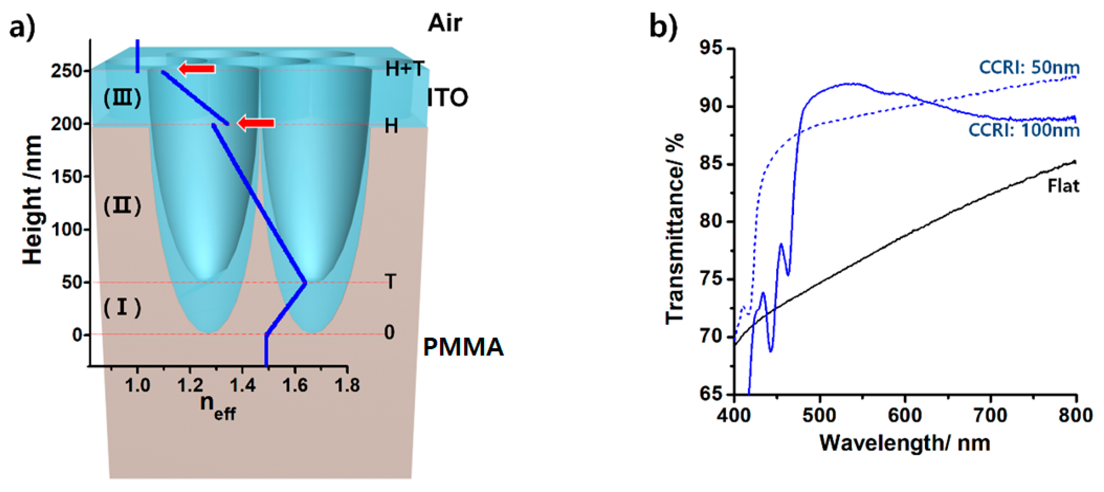
3. Results and Discussion

The reflection at the interfaces in the CCRI ITO film is governed by the refractive index profile along the film thickness direction, from the top air to the bottom substrate. The effective refractive index profiles of the corresponding structure to the CCRI ITO film are shown in Figure 3a. Assuming that the ARS is the subwavelength structure, that is, assuming the lattice period (d) of ARS is sufficiently smaller than the wavelength of light in the medium (d < λ/n; at a low visible wavelength range, d > λ/n), according to the Bruggeman effective medium model, the effective refractive index (neff) of a plane of any specific height (z) in the CCRI ITO film is given as follows [22,23]
f P M M A n P M M A 2 n e f f 2 n P M M A 2 + 2 n e f f 2 + f I T O n I T O 2 n e f f 2 n I T O 2 + 2 n e f f 2 + f a i r n a i r 2 n e f f 2 n a i r 2 + 2 n e f f 2 = 0
Here, f is the material fraction at z. nPMMA, nITO, and nair are 1.49, 2.19, and 1, respectively. As noted in Figure 3a, the z-axis is perpendicular to the PMMA film surface and the tips of pores in the N-ARS are at z = 0. H and T are the height of ARS and the thickness of the ITO layer, respectively. On the basis of its components, the CCRI ITO film can be divided into three different sections: section I (0 ≤ z < T) consisting of PMMA and ITO, section II (T ≤ z < H) consisting of PMMA, ITO, and air, and section III (H ≤ z ≤ H+T) consisting of ITO and air. In section I, fPMMA(z) + fITO(z) = 1 and fair(z) = 0; in section II, fPMMA(z) + fITO(z) + fair(z) = 1; and in section III, fITO(z) + fair(z) = 1 and fPMMA(z) = 0. Using these material fraction relations and equation (1), the effective refractive index profile of the CCRI ITO film with H = 200 nm and T = 50 nm has been calculated, as shown in Figure 3a. Owing to the tapered shape of ARS, it is possible to significantly reduce the abrupt refractive index change from air to the end of ARS. However, there are two refractive index discontinuities, at z = H and H + T, which is inevitable because there are abrupt changes of the material fraction.
As the ITO films are generally evaluated by the transmittance, the AR property of CCRI ITO films was confirmed by measuring the transmittance. The transmittance (normal incidence) of visible light through CCRI ITO films of the same (CCRI1, blue dotted line) and twofold greater (CCRI2, blue solid line) deposition time as employed for the 50 nm thick flat ITO film has been measured and the results are shown in Figure 3b. Compared to the flat ITO film (black line), the transmittance of both CCRI ITO films is significantly improved. The transmittance of the CCRI2 ITO film with similar electrical conduction to the flat ITO film varies from 69.3% to 92.8%. The average transmittance is 88.7%, which is 10.3% higher than that of the flat ITO film. The sudden decrease of transmittance over a range of 400–450 nm for the CCRI ITO films is ascribed to a diffraction phenomenon occurring at a low wavelength range where d > λ/n. Since various factors such as d, H, T, and the nipple diameter are precisely tunable, further enhancement of the optical transmittance of the CCRI ITO film (to the UV region of 400 nm or less) can be expected.

4. Conclusions

In summary, a new architecture has been designed to efficiently eliminate the reflection at the interfaces of multilayer-based optical systems. A complex continuous refractive index structured ITO film that alleviates the sudden refractive index changes in the existing ITO films was successfully fabricated. The obtained film showed significantly enhanced optical transmittance while maintaining high electrical conduction. Furthermore, delicate processes can subsequently be performed, and thus the AR ITO film is expected to significantly enhance the optical performance of various optoelectronic devices.

Author Contributions

K.C. conceived, designed and analyzed the experiments; K.C. conducted the experiments with J.J., J.K. and J.L.; H.S.L. advised on the experiments; K.C. and I.-S.K. wrote the manuscript with comments and input from all authors, and directed the project. All authors have read and agreed to the published version of the manuscript.

Funding

This work was supported by the Industry technology R&D program (20006476) funded by Ministry of Trade, Industry & Energy (MOTIE, Korea). This research was also funded by MINISTRY of LAND, INFRASTRUCTUR and TRANSPORT of KOREAN GOVERNMENT, grant number 17CTAP-C133309-01.

Conflicts of Interest

The authors declare no conflict of interest.

References

  1. Reineke, S.; Lindner, F.; Schwartz, S.; Seidler, N.; Walzer, K.; Lussem, B.; Leo, K. White organic light-emitting diodes with fluorescent tube efficiency. Nature 2009, 459, 234–238. [Google Scholar] [CrossRef]
  2. Sakthivel, P.; Murugan, R.; Asaithambi, S.; Karuppaiah, M.; Vijayaprasath, G.; Rajendran, S.; Hayakawa, Y.; Ravi, G. Studies on optoelectronic properties of magnetron Sputtered cadmium stannate (Cd2SnO4) thin films as alternative TCO materials for solar cell applications. Ceram. Int. 2018, 44, 2529–2538. [Google Scholar] [CrossRef]
  3. Caruge, J.M.; Halpert, J.E.; Wood, V.; Bulovic, V.; Bawendi, M.G. Colloidal quantum-dot light-emitting diodes with metal-oxide charge transport layers. Nat. Photonics 2008, 2, 247–250. [Google Scholar] [CrossRef]
  4. Sun, Y.; Forrest, S.R. Enhanced light out-coupling of organic light-emitting devices using embedded low-index grids. Nat. Photonics 2008, 2, 483–487. [Google Scholar] [CrossRef]
  5. Wu, W.-Q.; Feng, H.-L.; Chen, H.-Y.; Kuang, D.-B.; Su, C.-Y. Recent advances in hierarchical three-dimensional titanium dioxide nanotree arrays for high-performance solar cells. J. Mater. Chem. A 2017, 5, 12699–12717. [Google Scholar] [CrossRef]
  6. Yip, H.-L.; Hau, S.K.; Baek, N.S.; Ma, H.; Jen, A.K.-Y. Polymer Solar Cells That Use Self-Assembled-Monolayer-Modified ZnO/Metals as Cathodes. Adv. Mater. 2008, 20, 2376–2382. [Google Scholar] [CrossRef]
  7. Wu, Z.; Yang, Z.; Xue, K.; Fei, C.; Wang, F.; Yan, M.; Zhang, H.; Ma, D.; Huang, W. Performance enhancement of single layer organic light-emitting diodes using chlorinated indium tin oxide as the anode. RSC Adv. 2018, 8, 11255–11261. [Google Scholar] [CrossRef]
  8. Ham, E.V.D.; Elen, K.; Bonneux, G.; Maino, G.; Notten, P.; Van Bael, M.; Hardy, A. 3D indium tin oxide electrodes by ultrasonic spray deposition for current collection applications. J. Power Sources 2017, 348, 130–137. [Google Scholar]
  9. Kim, H.; Gilmore, C.M.; Horwitz, J.S.; Piqué, A.; Murata, H.; Kushto, G.P.; Schlaf, R.; Kafafi, Z.H.; Chrisey, D.B. Transparent conducting aluminum-doped zinc oxide thin films for organic light-emitting devices. Appl. Phys. Lett. 2000, 76, 259–261. [Google Scholar] [CrossRef]
  10. Batzill, M.; Diebold, U. The surface and materials science of tin oxide. Prog. Surf. Sci. 2005, 79, 47–154. [Google Scholar] [CrossRef]
  11. Walheim, S. Nanophase-Separated Polymer Films as High-Performance Antireflection Coatings. Science 1999, 283, 520–522. [Google Scholar] [CrossRef] [PubMed] [Green Version]
  12. Poitras, D.; Dobrowolski, J.A. Toward perfect antireflection coatings. 2. Theory. Appl. Opt. 2004, 43, 1286–1295. [Google Scholar] [CrossRef]
  13. Chhajed, S.; Schubert, M.F.; Kim, J.K.; Schubert, E.F. Nanostructured multilayer graded-index antireflection coating for Si solar cells with broadband and omnidirectional characteristics. Appl. Phys. Lett. 2008, 93, 251108. [Google Scholar] [CrossRef] [Green Version]
  14. Choi, K.; Yoon, Y.; Jung, J.; Ahn, C.W.; Lee, G.J.; Song, Y.M.; Ko, M.J.; Lee, H.S.; Kim, B.; Kang, I.-S. Antireflective Films: Super-Antireflective Structure Films with Precisely Controlled Refractive Index Profile. Adv. Opt. Mater. 2017, 5, 1600616. [Google Scholar] [CrossRef]
  15. Kim, J.K.; Chhajed, S.; Schubert, M.F.; Schubert, E.F.; Fischer, A.J.; Crawford, M.H.; Cho, J.; Kim, H.; Sone, C. Light-Extraction Enhancement of GaInN Light-Emitting Diodes by Graded-Refractive-Index Indium Tin Oxide Anti-Reflection Contact. Adv. Mater. 2008, 20, 801–804. [Google Scholar] [CrossRef]
  16. Yu, H.K.; Dong, W.J.; Jung, G.H.; Lee, J.-L. Three-Dimensional Nanobranched Indium–Tin-Oxide Anode for Organic Solar Cells. ACS Nano 2011, 5, 8026–8032. [Google Scholar] [CrossRef]
  17. O’Dwyer, C.; Szachowicz, M.; Visimberga, G.; Lavayen, V.; Newcomb, S.B.; Torres, C.M.S. Bottom-up growth of fully transparent contact layers of indium tin oxide nanowires for light-emitting devices. Nat. Nanotechnol. 2009, 4, 239–244. [Google Scholar] [CrossRef] [Green Version]
  18. Choi, K.; Park, S.H.; Song, Y.M.; Lee, Y.T.; Hwangbo, C.K.; Yang, H.; Lee, H.S. Nano-tailoring the Surface Structure for the Monolithic High-Performance Antireflection Polymer Film. Adv. Mater. 2010, 22, 3713–3718. [Google Scholar] [CrossRef]
  19. Choi, K.; Park, S.H.; Song, Y.M.; Cho, C.; Lee, H.S. Robustly nano-tailored honeycomb structure for high-throughput antireflection polymer films. J. Mater. Chem. 2012, 22, 17037. [Google Scholar] [CrossRef]
  20. Song, Y.M.; Jang, S.J.; Yu, J.S.; Lee, Y.T. Bioinspired Parabola Subwavelength Structures for Improved Broadband Antireflection. Small 2010, 6, 984–987. [Google Scholar] [CrossRef]
  21. Aberle, A.G.; Harder, N.P.; Oelting, S. Recent advances in crystalline silicon film and thin-film solar cell growth by ion-assisted deposition. In Proceedings of the 17th European Photovoltaic Solar Energy Conference, Munich, Germany, 22–26 October 2001; p. 1432. [Google Scholar]
  22. Luo, R. Effective medium theories for the optical properties of three-component composite materials. Appl. Opt. 1997, 36, 8153–8158. [Google Scholar] [CrossRef] [PubMed]
  23. Astrova, E.; Tolmachev, V. Effective refractive index and composition of oxidized porous silicon films. Mater. Sci. Eng. B 2000, 69, 142–148. [Google Scholar] [CrossRef]
Figure 1. Schematic diagrams showing the structures of the conventional λ/4 antireflection (AR) coating transparent conductive oxide (ITO) film (a) and the nano-porous ITO film (b) and highly branched ITO nanowire film (c) and the new structure for an ideal complex continuous refractive index (CCRI) ITO film designed in this work (d).
Micromachines 11 00206 g001
Figure 2. (a) Fabrication process of CCRI ITO film. (b) AFM height image of GaAs template having paraboloid-shaped nipples. (c) Top and cross-sectional SEM images of CCRI ITO film. An enlarged image is provided in the inset.
Micromachines 11 00206 g002
Figure 3. (a) Effective refractive index profile (neff, blue line) of CCRI-ITO film along the film thickness direction. The refractive index discontinuities are indicated by the red arrows. (b) Optical transmittance over the visible wavelength range for CCRI-ITO films with the same (CCRI1, blue dotted line) and twofold higher (CCRI2, blue solid line) deposition time as the 50 nm thick flat ITO film (transmittance indicated by black line).
Micromachines 11 00206 g003

