Article

Flexible Copper Mesh Electrodes with One-Step Ball-Milled TiO2 for High-Performance Dye-Sensitized Solar Cells

1
Sustainable Energy & Power Systems Research Center (RISE), University of Sharjah, Sharjah P.O. Box 27272, United Arab Emirates
2
Faculty of Engineering, International University for Science and Technology, Ghabageb 12710, Syrian Arab Republic
3
Department of Chemical Engineering, American University of Sharjah, Sharjah P.O. Box 26666, United Arab Emirates
4
Sustainable and Renewable Energy Engineering Department, University of Sharjah, Sharjah P.O. Box 27272, United Arab Emirates
*
Author to whom correspondence should be addressed.
Sustainability 2025, 17(21), 9478; https://doi.org/10.3390/su17219478 (registering DOI)
Submission received: 3 September 2025 / Revised: 5 October 2025 / Accepted: 21 October 2025 / Published: 24 October 2025

Abstract

Advancements in flexible, low-cost, and recyclable alternatives to transparent conductive oxides (TCOs) are critical challenges in the sustainability of third-generation solar cells. This work introduces a copper mesh-based transparent electrode for dye-sensitized solar cells, replacing conventional fluorine doped-tin oxide (FTO)-coated glass to simultaneously reduce spectral reflection losses, enhance mechanical flexibility, and enable material recyclability. Titanium dioxide (TiO2) photoanodes were synthesized and directly deposited onto the mesh via a single-step, low-energy ball milling process, which eliminates TiO2 paste preparation and high-temperature annealing while reducing fabrication time from over three hours to 30 min. Structural and surface analyses confirmed the deposition of high-purity anatase-phase TiO2 with strong adhesion to the mesh branches, enabling improved dye loading and electron injection pathways. Optical studies revealed higher visible light absorption for the copper mesh compared to FTO in the visible range, further enhanced upon TiO2 and Ru-based dye deposition. Electrochemical measurements showed that TiO2/Cu mesh electrodes exhibited significantly higher photocurrent densities and faster photo response rates than bare Cu mesh, with dye-sensitized Cu mesh achieving the lowest charge transfer resistance in impedance analysis. Techno–economic and sustainability assessments revealed a decrease of 7.8% in cost and 82% in CO2 emissions associated with the fabrication of electrodes as compared to conventional TCO electrodes. The synergy between high conductivity, transparency, mechanical durability, and a scalable, recyclable fabrication route positions this architecture as a strong candidate for next-generation dye-sensitized solar modules that are both flexible and sustainable.

1. Introduction

In recent years, renewable and sustainable energy systems have gained more prominence and importance within the energy mix, and this is primarily driven by the rising need for power and energy. Initially designed to complement the main grid and address periods of high demand, these systems are now being explored as a feasible choice for a self-sufficient continuous power supply. This aligns with initiatives to lower greenhouse gas emissions and promote sustainable electricity generation. Among the various renewable energy sources, solar power—specifically solar photovoltaic (PV) systems—holds the highest popularity due to its ability to directly convert solar energy into electricity [1]. The technology behind PV systems has made significant strides in terms of cost-effectiveness, thanks to developments in cell materials, module production, and large-scale distribution [2].
Typically composed of crystalline silicon, first-generation solar cells are widely available in the market. Despite their commercial prevalence, these cells are inundated by certain drawbacks such as high expenses, fragility, and restricted design adaptability [3]. The following generation of PV systems encompass thin-film technologies that are also commonly found in the market. These include copper indium gallium selenide, cadmium telluride, gallium arsenide, and amorphous silicon [4]. Third-generation PV systems encompass an array of emerging technologies that aim to surmount the limitations of the first- and second-generation systems. These innovations are built upon dye-sensitized solar cells (DSSCs), organic solar cells (OSCs), and perovskite solar cells (PSCs) [5]. Third-generation solar cells allow for novel and creative applications, including see-through solar cells suitable for incorporation into windows, adaptable solar cells suitable for integration into garments or other portable gadgets, and dye-sensitized solar cells capable of serving indoor lighting needs. Furthermore, these advanced solar cells have the potential to decrease the environmental footprint connected with the fabrication of the devices, and can thus address concerns like the utilization of harmful substances and risky chemicals [6]. DSSCs, also known as Grätzel cells [7], present a unique and innovative approach to harnessing solar energy. These photovoltaic devices utilize a layered structure composed of a semiconducting photoanode, a counter electrode, and active materials presented by an electrolyte and an absorbing dye. Its cost-effective manufacturing process, which involves simple fabrication techniques and the use of abundant materials, is considered as one of the main advantages of DSSCs [8].
The significant benefit of DSSCs lies in the capability to enhance cell performance through the optimization of various components, including electron transport and active materials, counter electrodes, and photoanodes. Semiconducting metal oxides such as titanium oxide (TiO2) and zinc oxide (ZnO) are commonly used to make electron transport material in DSSCs [9]. In an attempt to boost the kinetics of electron transportation, the addition of nanoparticles has been investigated. For instance, dispersing graphene microplatelets and copper nanopowder on a TiO2 layer resulted in efficiency increases of up to 30% and 53.7%, respectively [10,11]. Holmium-doped TiO2 and ZnO nanomaterials and co-doped TiO2 with Zn and Cu have been synthesized and used as electron transport materials, resulting in an efficiency increase of up to 1.51% and 3%, respectively [12,13]. Natural and green dyes, derived from plants and natural resources, have been studied as an economical and environmentally friendly alternative to conventional ruthenium-based dyes utilized in DSSCs. For instance, Peltophorum pterocarpum leaves were used to extract natural dyes and showed a DSSC efficiency of 6.07% [14]. Additionally, Calotropis plants, which are harmful non-food plants, were investigated as a dye source, resulting in a solar cell efficiency of 0.214% [15]. Further research investigated the effect of the Calotropis leaves’ orientation on the performance of DSSCs and revealed that plant leaves facing west reported the highest efficiency of 0.157% [16]. Sinha et al. [17] tested devices with natural dyes obtained from cabbage, spinach, and turmeric, and their combination, and obtained efficiencies of 0.1%, 0.13%, 0.30%, and 0.6%, respectively.
The preferred electrodes in DSSCs are typically glass substrate coated with fluorine-doped tin oxide (FTO) in the case of photoanodes, or coated with platinum or gold in the case of the counter electrode [18]. Platinum (or gold) metals serve as a catalyst, aiding in the dye regeneration process. Nevertheless, due to their high cost, research has been directed towards discovering more economical and suitable sustainable alternatives, such as carbon-based materials. For instance, a DSSC with a counter electrode fabricated from a reduced graphene oxide layer reported an efficiency of 9.22% [19]. Moreover, transition metal dichalcogenides like tungsten disulfide and molybdenum disulfide revealed great potential as counter electrodes [20]. Tellurium-doped graphene (Te-Gr) resulted in a 28% increase in efficiency compared to Pt-based counter electrodes [21]. Fiber-shaped DSSCs have also been investigated by integrating two transition metal dichalcogenide materials onto a conductive fibrous substrate, in order to enhance the electrocatalytic activity, interfacial contact, and mechanical robustness of the counter electrode [22]. These DSSCs showed an efficiency of 8.90% and a long-term stability, retaining 90.1% of the initial efficiency after approximately 1000 h.
Glass substrates offer a smooth and even surface, ensuring effective adhesion and uniform contact with subsequently deposited layers. While glass maintains excellent solar radiation transmission, FTO also provides electronic conductivity to the photoanode, facilitating the collection and transport of electrons to an external load. Although this arrangement is conventional, there are efficiency losses due to decreased transmissivity from the reflection of incoming radiation on the glass surface. Additionally, FTO exhibits relatively higher resistivity compared to opaque metals, in addition to its rigid structure that offers no flexibility. Hence, numerous studies have investigated the fabrication of flexible DSSCs. Thus, several metals have been studied as potential electrodes for DSSC applications. Ismail et al. [23] examined the effect of bending angle on DSSC performance using a Ti foil photoanode and ITO-PET counter electrode under back-illumination conditions. The results reported a maximum conversion efficiency of 2.03%, with device performance remaining stable up to a bending angle of 20°, beyond which efficiency declined due to surface cracking and microstructural damage on the TiO2/Ti substrate. Putra et al. [24] employed TiO2 P25 films on a flexible ITO/PET substrate for utilization as a photoanode. The device was fabricated through screen printing and hot-pressing methods and achieved a conversion efficiency of 0.29%. Khir et al. [25] developed a flexible photoanode through screen printing of TiO2-Bithmus inks. This modification reduced resistance by 57–65%, suppressed recombination, and extended electron lifetime (0.0036 ms). Jin et al. [26] reported a low-temperature approach for integrating a metal–organic framework into flexible DSSCs made from ITO-PEN photoanodes. The devices showed fast electron diffusion and an efficiency of 4.41%. Opaque metals have also been utilized as photoanode material. For instance, silver (Ag) garnered significant attention for its application as a counter electrode, especially as Ag nanowires [27]. Nevertheless, the high cost associated with the mass production of Ag remains a substantial concern. Therefore, it is worth noting that copper (Cu), in particular Cu mesh, can be an alternative due to its feasibility and elevated electrical conductivity, as well as mechanical and electrical stability [28]. In addition, Cu substrates can be easily and effectively coated with various materials in order to enhance corrosion resistance and behavior [29,30]. For instance, the efficiency of a DSSC increased by 260% when Cu2S mesh was utilized as a counter electrode [31]. The use of Cu mesh as an electrode in solar cells enables the fabrication of flexible devices with improved efficiency, such as a flexible DSSC with TiO2/CuI/Cu mesh. Such a device exhibited outstanding mechanical stability and performance, with an efficiency of 4.73% [32]. Cu meshes can also enhance the visible photocatalytic properties of devices, as demonstrated by growing Cu sulfide and Cu oxide nanowire heterostructures on copper mesh, which showed efficient degradation of dye under visible light irradiation [33]. For instance, efficiencies of 87.4% and 98.6% were recorded after 20 min and 40 min, respectively [33].
In this paper, the viability of Cu mesh as a promising substitute for FTO-coated glass in DSSC photoelectrodes is explored. It is anticipated that the resulting cell will outperform conventional FTO setups due to the low cost, flexibility, enhanced strength, and conductivity offered by Cu meshes. A TiO2 layer is deposited on the mesh, employing ball milling, which is a technique that offers a facile and one-step process for the synthesis and deposition of the TiO2 layer. Such a technique eliminates the necessity for the preparation of the TiO2 paste and the TiO2 film annealing, enabling the deposition of thin films with controlled thicknesses. This presents distinct advantages compared to conventional techniques like doctor blading and screen printing. The inherent structure of the Cu mesh facilitates multi-directional interaction between incident radiation and the deposited TiO2/dye layers, thereby augmenting photon-to-electron conversions. The fabricated electrodes will be examined from various vantage points such as microstructural, spectral, and electrochemical, to quantify their potential for solar cell applications.

2. Experimental Materials and Methods

2.1. Electrodes Preparation

In this work, three variations of the electrodes are presented: Cu1, Cu2, and Cu3, resembling the treated Cu mesh, treated Cu mesh with TiO2 layer, and dye-sensitized/TiO2 layer Cu mesh, respectively. The preparation of the Cu mesh starts with cutting it into 5 × 5 cm pieces. The substrates are cleaned, first with ethanol and then with deionized (DI) water for a period of 15 min using an ultrasonic bath. The mesh is then rinsed, dried, and placed under UV–Ozone treatment for 30 min. Thermal treatment is then carried out to obtain copper oxide by annealing the Cu mesh substrates for 30 min at 450 °C under an open atmosphere. The deposition of the TiO2 layer on the treated Cu mesh is processed using the high-energy yet facile ball milling process. A known mass of nanoparticle-sized TiO2 powder is added to a crucible made from stainless steel with a volume of 25 mL. The Cu mesh is restricted on the edge of the crucible to ensure uniform deposition. The milling conditions are set to 450 rpm for a duration of 30 min. The ruthenium-based dye is prepared by dissolving a known amount of ruthenium into a certain volume of ethanol at a ratio of 0.3mg/mL. The dye is then introduced to the substrates by adsorption, and the Cu mesh/TiO2 substrates are immersed in the dye in a container that is placed in an unilluminated and dry room for a minimum period of 24 h. Figure 1 shows the process of fabricating and preparing the electrodes.
In order to assess the performance of the fabricated electrodes, a comparison with conventional FTO electrodes is carried out. The deposition of the TiO2 and Ru dye on the FTO is carried out through the methodology described in [15,21].

2.2. Electrode Characterization

The crystalline structure of the various electrodes is studied through X-ray diffraction (XRD) and is performed using the Bruker D8 Advance device (Manning Park Billerica, MA, USA). Raman spectra of the electrodes are recorded using a Renishaw InVia spectrophotometer (Stroud, UK), at a laser excitation wavelength of 514.5 nm with an acquisition time of approximately 30 s. The Raman spectra are utilized to study the structural and chemical characteristics of the various electrodes. X-ray photoelectron spectroscopy (XPS) is performed through a Nexsa G2 machine (Thermo Fisher Scientific Inc., Waltham, MA, USA), and is utilized to examine the elemental state and chemical compositions of the various electrode materials using mono-chromatized Al-Kα radiation (1486.6 eV) under ultra-high vacuum (~10–9 mbar). Scanning electron microscopy (SEM) is employed to investigate the deposition of the TiO2 layer and to study the surface characteristics of the electrodes. SEM is performed through the Tescan Vega machine (Brno, Czechia) under 15k magnification and a beam intensity of 20 kV.

2.3. Electrode Testing

The spectral absorbance of the various electrodes is measured in the UV–Vis spectrum via a Shimadzu UV-2600iUV–Vis spectrophotometer (Kyoto, Japan). The spectra are carried using the double beam mode and utilizing air as a background reference. Chronoamperometry analysis through the Bio-Logic SP300 potentiostat (Paris, France) is utilized to study the photo response of the electrodes. A three-electrode system is used in the analysis, where the variations in the Cu mesh (Cu1, Cu2, and Cu3) act as a working electrode, a platinum (Pt) substrate acts as the counter electrode with silver/silver chloride (Ag/AgCl) saturated in potassium chloride (KCl) acting as a reference electrode. Figure 2 shows the experimental setup.
The measurements are obtained at an open circuit voltage for a time interval of 10 min with both illuminated and dark cycles in a sodium hydroxide (NaOH) solution naturalized with hydrochloric acid (HCl). Throughout the testing process, the electrodes are kept at a fixed distance from the light source (tungsten lamp). The same setup is utilized to study the impedance of the electrodes and deduce the consequences of incorporating the TiO2 layer and the regenerative dye. The electrochemical impedance spectroscopy (EIS) measurements are recorded for frequencies in the range of 10 mHz to 0.1 MHz, with a resolution of 50 μV. The Z-fit tool, available on the EC-lab software, is employed to process the data in terms of fitting.

3. Results and Discussion

The following sections present the surface, elemental, and spectral characterization results of the fabricated electrodes. In addition, the photo response and electrochemical testing results are provided.

3.1. Elemental and Surface Characterization

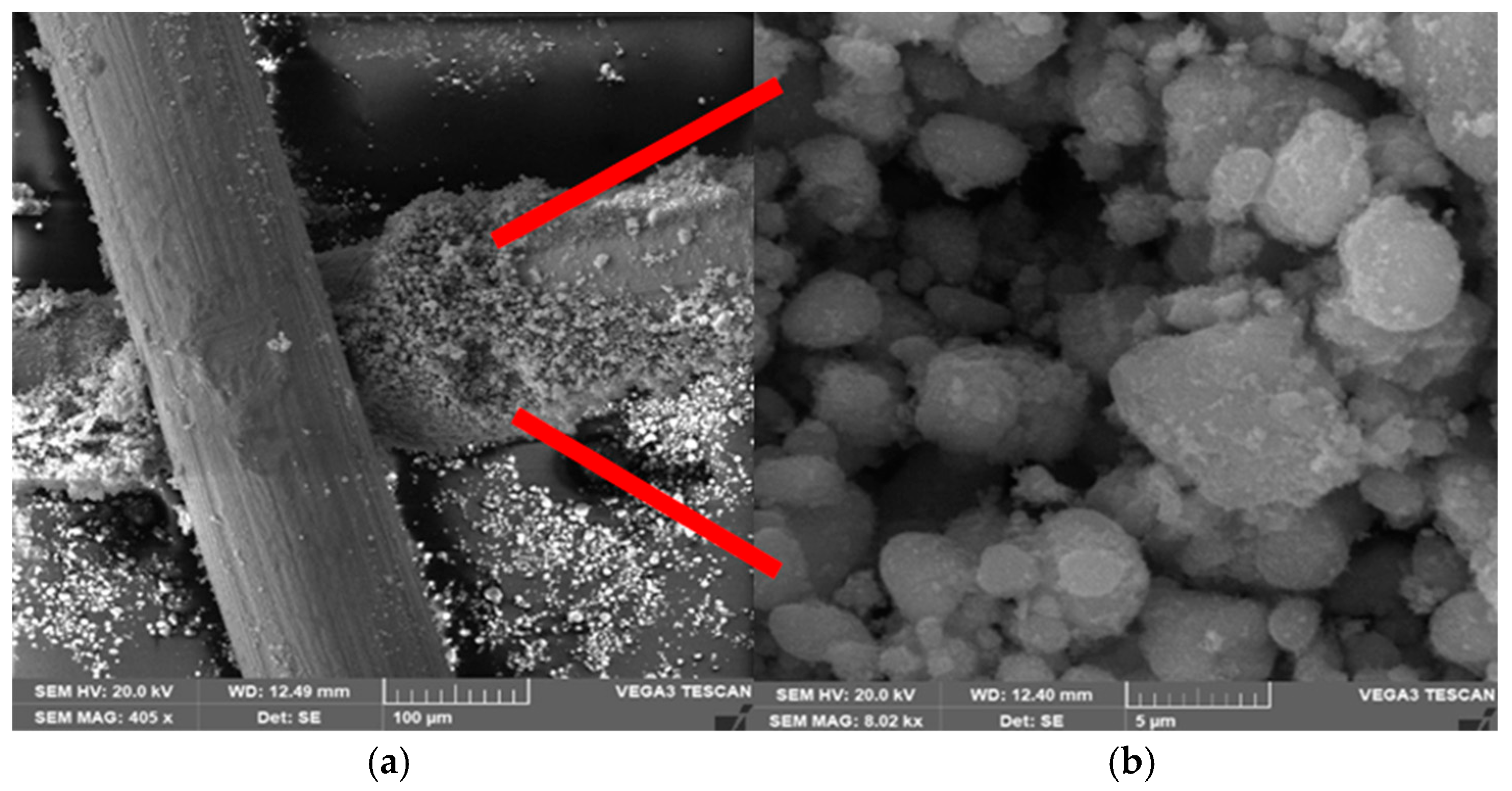
The deposition of the TiO2 nanoparticles at a microscale level is investigated using SEM, and information on the grain size and formation of the TiO2 layer are provided as well. Figure 3 shows the SEM images of the Cu mesh with TiO2 layer at various scales. The images are obtained with a beam intensity of 20 kV and magnification of 15k. The image on the right is the magnified TiO2 layer marked by the red arrows in the image of the left. Inspection of the images reveals that the TiO2 grains are tightly secured with the Cu mesh fingers, due to the sturdy, disordered arrangement of the substrate that promotes increased interaction between the surface and incoming solar radiation. Based on Gwyddion software analysis [34], the size of TiO2 grains is in the range of 3.3–4.2 μm, depending on the region and electrode. The SEM image also proves the successful deposition of the TiO2 layer on the Cu mesh. This outcome holds significance, as the strong bond between the TiO2 and the supporting Cu substrate will lead to reduced resistance in charge transfer.
Figure 4 displays the XRD spectra of the Cu1 and Cu2 electrodes with the Cu mesh and TiO2 layer. The XRD analysis is not conducted for the Cu3 electrode as Ru-based dyes cannot be directly detected by XRD, since they are molecular complexes that adsorb as ultrathin amorphous layers on the TiO2 surface. As such, they do not produce distinct crystalline diffraction peaks that can be resolved over the much stronger TiO2 signals. The results indicate the presence of copper and its oxides, which appear due to the thermal treatment. The presented peaks are in line with data that investigate the structure of copper mesh and its oxides [35]. In addition, the Cu mesh spectrum is aligned with the Cu card (ICDD 00-004-0836) obtained from the International Center for Diffraction Data (ICDD). Moreover, the spectra show the presence of the anatase-phase TiO2 which is favorable for solar cell and photo response applications given its high stability and surface area [36]. The presented peaks are sharp and narrow in shape which indicates the presence of TiO2 particles with high crystallinity. In addition, the XRD patterns verify that there are no impurities present from the surrounding environment during both the synthesis and deposition processes.
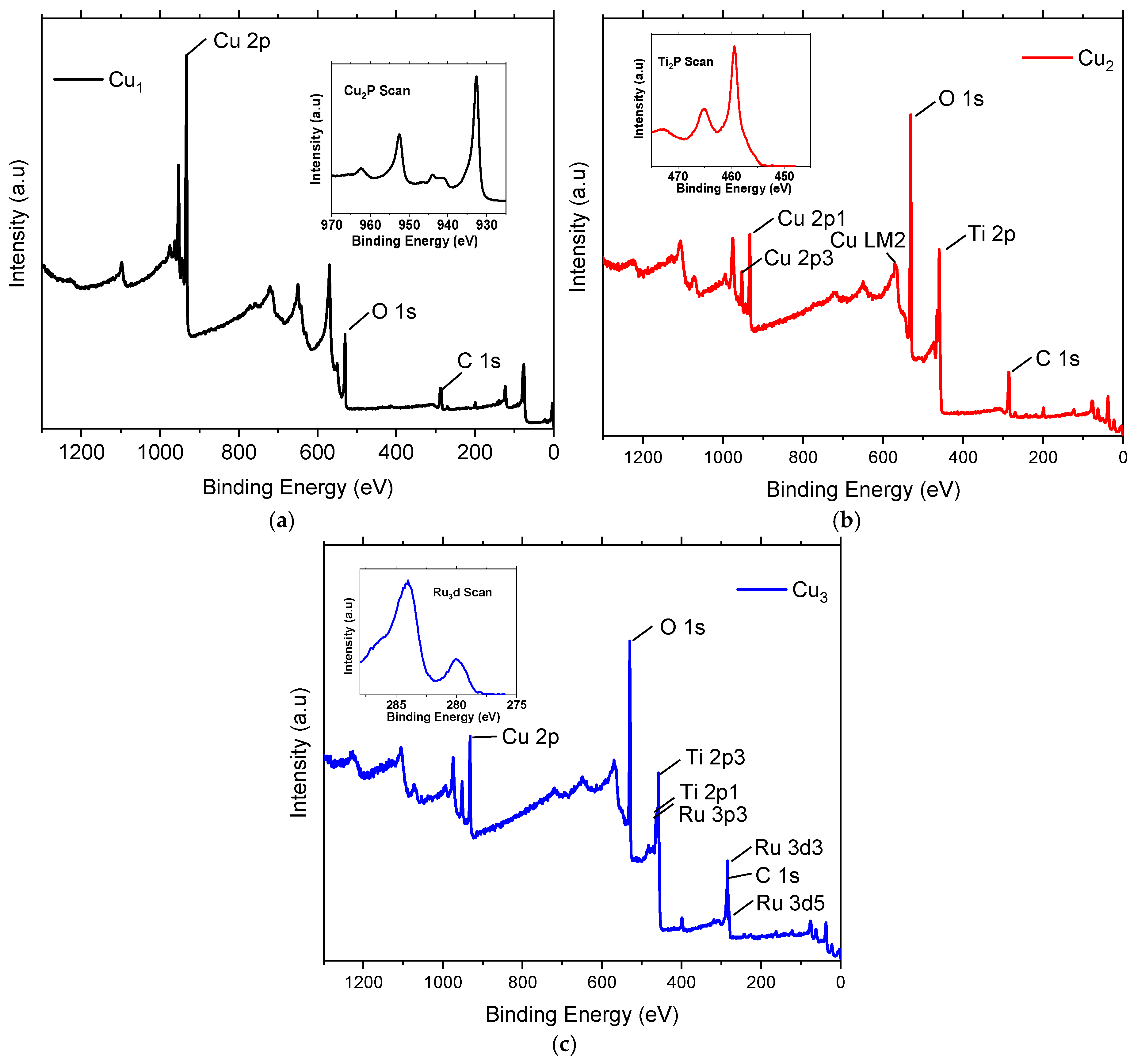
Figure 5 shows the measured XPS spectra survey of Cu1, Cu2, and Cu3 electrodes. In all cases, it is seen that the binding energy of the Cu 2p peaks is in the typical range of 932–934 eV [37]. Close inspection (inset graph in Figure 5a) reveals the presence of the characteristic doublet peaks related to Cu 2p1/2 and Cu 2p3/2 at ~ 952 eV and ~ 932 eV, respectively [38]. Figure 5b focuses on the XPS data of Cu2 electrodes, where peaks related to Cu 2p, Ti 2P, O 1s, and C 1s are present. Peaks related to Cu 2p are apparent because of the copper substrate and are comparable to those of Cu1 electrodes. A close up view of the Ti 2p peaks (seen in the inset of Figure 5b) shows binding energy peaks at 459 eV and 465 eV corresponding to Ti 2p3/2 and Ti 2p1/2 and are assigned to Ti4+ in TiO2 [39]. The presence of an O 1s peak in the vicinity of 530 eV is a typical representation of the Ti-O bonds on TiO2 [40]. These peaks are also apparent in the XPS spectrum of electrodes Cu3 shown in Figure 5c. In addition, inset of Figure 5c shows peaks corresponding to Ru 3d5/2 and Ru 3d3/2 and they are apparent at the binding energies of 280 eV and 284 eV, respectively. The peak around 280 eV can be assigned to the Ru0 metallic atom [41]. In all cases, the C 1s peak implies the presence of impurities and ambient contamination that are adsorbed on the electrodes.
Figure 6 displays the Raman scattering of the fabricated electrodes Cu1, Cu2, and Cu3. Raman is employed to confirm the phase of the deposited TiO2 layer and the presence of the sensitizing dye. Inspection of the Cu1 spectrum shows the presence of peaks in the vicinity of 215, 356, and 642 cm−1 which correspond to the phonon scattering of the three Raman active optical phonon branches Ag + 2Bg, respectively [38]. Regarding Cu2 electrodes, Raman is used to validate the purity of the synthesized anatase TiO2 layer. Six fundamental Raman active modes are identified, denoted as A1g + 2B1g + 3Eg, distinguishing it from the rutile phase which features four active modes A1g + 2B1g +B2g + 3Eg [42,43].
The Raman spectrum depicted in Figure 6 distinctly manifests characteristic attributes of TiO2 anatase, with discernible peaks at 144 (Eg), 197 (Eg), 399 (B1g), 513 (A1g), 519 (B1g), and 639 cm−1 (Eg). Thus, it can be proven that the high-purity anatase phase of TiO2 is attained via the ball milling method. The same peaks can be observed in the spectrum regarding the Cu3 electrode. Moreover, a peak around 700 cm−1 signaling the presence of the Ru-based sensitizing dye is observed [44]. In both Cu2 and Cu3 spectra, the peaks corresponding to the copper oxide are still present, yet they have diminished in amplitude, implying uniform and even deposition of the TiO2 layer over the Cu mesh substrate [37].

3.2. Photoelectrical Response

The UV–Vis absorption analysis of the fabricated electrodes, presented in Figure 7, reveals a noteworthy advantage in employing copper mesh as an electrode material compared to the conventional choice, FTO. Cu electrodes exhibit superior absorption within the visible light range (400–800 nm), whereas FTO demonstrates higher absorption in the UV region (200–400 nm), with absorbance intensities reaching 4–5 (a.u), especially when compared to Cu1 and Cu2 electrodes. The incorporation of a TiO2 layer significantly enhances the absorption of the Cu mesh electrodes, as evident in the absorption spectra of Cu1 and Cu2 electrodes, where an enhancement of 0.3 (a.u) is recorded. It was expected that there would be a decrease in absorption for the Cu2 electrode in the 450–750 nm range, given the greater activity of TiO2 when closer to UV light. To address these limitations, the addition of the Ru-based dye becomes crucial. Notably, the Cu3 electrode displays the highest light absorption across the UV–Vis spectrum.
The UV–Vis spectra confirm the successful and uniform deposition of the TiO2 layer, achieved through ball milling and establishing Cu mesh-based electrodes as a promising alternative to conventional materials like FTO. These results are promising, particularly considering the porous nature of the Cu mesh. Thus, the UV–Vis spectra affirm that in comparison to FTO, the light irradiation is highly absorbed in the Cu mesh due to the scaffolding-like structure, which also boasts higher reflectance properties. These attributes ensure proper dispersion of light irradiation onto the substrate hosting the light active materials such as the TiO2 layer and the sensitized dye. Additionally, due to the commendable thermal conductivity of the Cu mesh, any emitted radiation dissipates rapidly, thereby not contributing to heat-induced degradation of the substrate. The optical transparency of the fabricated electrodes is also evaluated using UV–Vis spectroscopy. The transmittance profile across the visible region provides a direct measure of transparency, with lower absorbance corresponding to higher optical transmission. This confirms that the UV–Vis data not only demonstrate enhanced light absorption upon TiO2/dye deposition but also serve as a quantitative indicator of the electrode’s transparency.
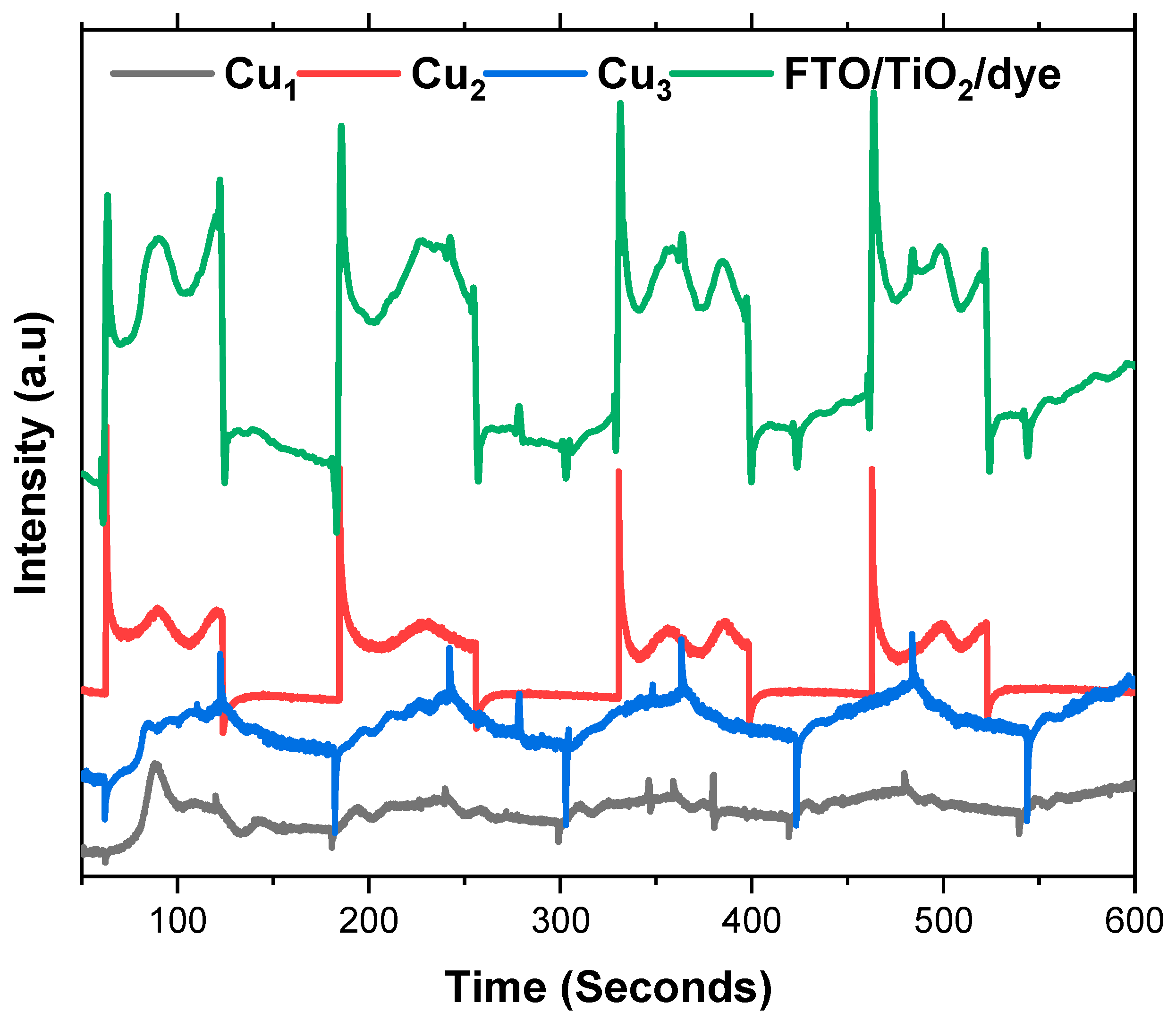
The photoelectric response of the electrodes is studied through chronoamperometry by applying a light source at various time intervals. Figure 8 shows the photocurrent response of the Cu1, Cu2, and Cu3 electrodes, in addition to the conventional FTo/TiO2/Ru dye electrode. Cu1 electrodes show adequate photo response as the Cu mesh is thermally annealed, and a semiconducting oxide is formed. Nevertheless, the addition of the TiO2 layer (Cu2 electrodes) greatly enhances the photocurrent of the Cu mesh electrodes and the photo response rate. This increase is a result of the improved charge separation and transport, which is seen with the addition of the TiO2 that has a wider bandgap than the Cu mesh oxide. Moreover, the introduction of Ru-based dye aids in the increase in the photocurrent and photo response of the electrodes. The utilization of the dye improves the electron injection rate, as the excited state of the ruthenium dye allows electrons to easily inject into the conduction band of the TiO2 layer. This accelerates the charge separation process, leading to a higher photo response rate. Furthermore, by efficiently injecting electrons, the ruthenium dye helps to minimize the recombination of charge carriers, which occurs when electrons and holes recombine rather than contribute to the current. In comparison, the FTO/TiO2/dye electrode delivers the largest, most reproducible on/off signals with sharp rise spikes followed by high, stable plateaus, reflecting fast injection from the dye, efficient percolation of electrons through the TiO2 network, and low-resistance collection by the FTO substrate.
Impedance spectroscopy is utilized to study the electrical behavior of solar cells under various conditions. This includes crucial parameters such as series resistance, shunt resistance, capacitance, and ideality factors, which are essential for understanding losses and efficiency limitations. Additionally, impedance spectroscopy aids in studying carrier dynamics, characterizing interfaces, detecting degradation, and optimizing device performance. The interface between the Cu mesh, TiO2 layer, and regenerative dye is modeled based on the equivalent circuit shown in the inset of Figure 9. Given the unconventional structure of the Cu mesh, its double-layer capacitance is modeled as a Constant Phase Element (CPE). The charge transfer resistance at the Cu mesh/active layer (TiO2/dye) interface is modeled by Rct. The series resistance (Rs) represents the overall resistance associated with the Cu mesh, including any resistance due to the metal itself and any contact resistances.
Figure 9 illustrates the Nyquist plot depicting the behavior of Cu1, Cu2, and Cu3 electrodes. While a semicircular pattern is typically observed in most electrochemical systems, the distinctive structure of the Cu mesh leads to a deviation in the Nyquist plot. Nonetheless, the plot yields valuable insights into the interactions at the interface of the Cu mesh, TiO2 layer, and Ru-based dye. The diameter of the semicircle directly correlates with the system’s charge transfer resistance, with a smaller diameter indicating more efficient charge transfer processes. Table 1 shows a summary of the series and charge transfer resistances of the various electrodes. Rs is estimated from the x-axis intercept at the start of the curve, while Rct is estimated from the width of the semicircle along the x-axis (difference between the start and end of the arc).
The Nyquist plots clearly reveal distinct electrical behaviors for the three electrode configurations. For the bare copper mesh electrode (Cu1), the series resistance is approximately 90 Ω, with a relatively high charge transfer resistance of about 900 Ω. These values suggest that while the Cu mesh provides baseline conductivity, significant barriers remain for efficient electron transfer at the electrode–electrolyte interface. Upon introducing the TiO2 layer as seen in electrode Cu2, Rs decreases slightly to 80 Ω, indicating improved interfacial contact and reduced overall ohmic losses. More importantly, the Rct is reduced to 800 Ω, which highlights the beneficial role of TiO2 in enhancing charge separation and facilitating electron injection. However, despite this improvement, the charge transfer resistance remains comparatively high, implying that further optimization is needed to minimize recombination processes. The most notable performance enhancement is observed for the dye-sensitized Cu mesh electrode Cu3. Here, Rs drops further to 70 Ω, while Rct decreases significantly to 380 Ω, which is less than half that of the untreated mesh. The high reduction demonstrates the synergistic effect of combining the conductive copper mesh with a high-purity anatase TiO2 layer and an efficient Ru-based dye. The dye not only enhances light absorption but also accelerates electron injection into TiO2, thereby reducing recombination and improving overall charge transfer kinetics. Despite the non-standard shapes, it is evident that Cu3 electrodes exhibit the closest approximation to a semicircle, implying superior charge transfer resistance compared to Cu1 and Cu2 electrodes.

3.3. Techno–Economic and Sustainability Assessment

In order to completely evaluate the viability of the Cu mesh electrodes, an economical and environmental analysis investigating the materials cost and fabrication process is carried out. Table 2 shows the bill and cost of the materials utilized for the fabrication of the conventional and flexible DSSCs based on Cu mesh electrodes. The prices are based on quotations from local suppliers, and a batch of DSSCs contains 10 different cells. The materials are separated into materials for the photoanode electrodes and for the sensitizer and counter electrode. For both conventional and flexible DSSCs, the sensitizer and counter electrode materials are the same. It can be seen that due to the low cost of Cu mesh, the total price for the fabrication of flexible DSSCs is lower than that of conventional DSSCs. Moreover, the ball milling technique requires less amounts of TiO2 as the synthesis and deposition are both achieved in one step, reducing losses and the amount of material needed.
Table 3 shows the cost of electricity and CO2 emissions associated with the fabrication of the conventional (FTO) and flexible electrodes. The cost linked to energy consumption is determined as 0.367 United Arab Emirates Dirham (AED) per kWh, aligning with the electricity tariff of the Dubai Electricity and Water Authority [45], while the CO2 emissions of electricity are estimated as 0.8 kg/kWh [46]. The utilization of the facile ball milling technique not only simplifies the synthesis and the deposition of the TiO2 into one step but also reduces the total time taken for the fabrication by almost an hour and a half. This reduction is manifested by a lower electricity cost and CO2 emission for the fabrication of the Cu mesh electrodes.
In order to assert metallic-based electrodes as a viable alternative for conventional electrodes, an industry-oriented comparison of common commercially available photoanodes is carried out. Table 4 shows a summarized comparative analysis between commercially available glass electrodes, and polymer-based and metallic-based electrodes [47,48,49,50,51,52,53,54,55,56]. The comparison highlights three distinct value propositions across the electrode classes. The trade space is governed by the conductivity and transparency figure of merit, electrochemical durability, and manufacturability. FTO on glass delivers the most stable optoelectronic baseline with negligible drift under illumination, heat, and oxidizing electrolytes. Nevertheless, intrinsically mechanical limitations such as brittleness and poor flexural endurance, in addition to high process temperatures, constrain substrate applications. Thus, glass is suitable for rigid modules and benchmarking, but it is less than ideal for flexible or low-temperature stacks. Polymer electrodes such as PEDOT: PSS invert those constraints with low solution processing temperatures, and roll-to-roll manufacturing compatibility which enables low-CAPEX and large-area coating with excellent bendability. However, the achievable conductivity and transparency is typically inferior to FTO, or metal meshes at comparable transmittance. Additionally, moisture, oxygen, UV, and acidic formulations accelerate conductivity loss unless barrier layers and post-treatments are employed. Metallic meshes (e.g., Cu) with conformal TiO2 passivation and Ru dye sensitization achieve the highest current headroom because series resistance can approach the milliohm regime while the optical aperture remains high. If the TiO2 layer is dense and continuous, it functions as both an electron-selective layer and as a corrosion barrier, reducing recombination at the metal/electrolyte interface and enabling dye-assisted injection into the TiO2 conduction band. Nevertheless, incomplete coverage or rough edges can dominate failure through localized pitting and rising dark currents.
Recommendations follow from these constraints. For instance, applications prioritizing metrological stability, long operational lifetimes, and straightforward benchmarking, FTO/TiO2/Ru-dye remains the preferred architecture. For flexible or temperature-limited substrates, polymer electrodes are viable provided the stack includes (i) neutralized/high-conductivity PEDOT: PSS, (ii) an inorganic or multilayer moisture/oxygen barrier and (iii) UV filtering or stabilizers. Even with these recommendations, lower peak photocurrents are expected, and encapsulation costs need to be planned for. In cases where flexibility is required and maximum photo response per materials cost is the objective, a Cu-mesh/TiO2/Ru-dye stack is advantageous if process control is available. A well-deposited thin and dense TiO2 film is essential to act as a passivation layer and prevent under-film ingress.
From a sustainability and end-of-life perspective, glass offers durability and recyclability if the device is designed for clean delamination; nevertheless, the remelting process is heavy and energy intensive. Polymer substrates enable low-temperature and lightweight manufacturing, yet once laminated with metals and oxides, it becomes hard to separate. Thus, these substrates are usually downcycled or incinerated unless a validated mono-material or chemical-recycling route exists. Cu mesh exhibits a robust circular end-of-life pathway, with high residual value and efficient recovery via mature smelting and refining infrastructure. Given the elevated impacts of primary copper production, substrates should target highly recycled content and incorporate strippable passivation layers to enable clean reclamation and minimize corrosion.

4. Conclusions

This work demonstrates the successful fabrication of copper mesh-based electrodes for DSSCs, evaluated through structural, optical, and electrochemical characterization, and in addition to applying techno–economic and sustainability assessments to assess the viability of the electrodes as an alternative to conventional FTO on glass electrodes. Three electrode configurations were investigated: pristine copper mesh, TiO2-coated copper mesh, and dye-sensitized TiO2/copper mesh. The TiO2 layer was deposited using a one-step ball milling process, which effectively simplified electrode fabrication by eliminating the need for paste preparation and high-temperature annealing. Compared to traditional doctor blading or screen printing methods that require several hours, the proposed approach achieved both synthesis and deposition in just 30 min, significantly reducing time and energy consumption. Structural analyses (XRD, Raman, XPS, SEM) confirmed the formation of high-purity anatase TiO2, with uniform adhesion on the copper mesh branches, enabling enhanced dye adsorption and efficient electron injection.
The results highlight that the copper mesh substrate offers clear advantages over conventional FTO/glass electrodes. In terms of fabrication, the Cu mesh electrodes show a lower cost (7.8%) and less CO2 emission (82%) as compared to conventional electrodes. The copper mesh’s distinctive open structure enhances optical transparency, reduces sheet resistance, and provides superior electrical conductivity. Moreover, the flexibility, recyclability, and mechanical stability of copper mesh make it well suited for the development of next-generation flexible and sustainable solar cells. Electrochemical impedance spectroscopy confirmed improved charge transfer characteristics for the dye-sensitized TiO2/copper mesh configuration, correlating with enhanced photocurrent generation and reduced recombination losses.
The study establishes copper mesh electrodes combined with one-step ball-milled TiO2 deposition as a promising alternative to glass/TCO-based DSSCs. Beyond simplifying fabrication, this approach enables scalable, modular device designs, where multiple cells can be integrated on a single mesh substrate in series or parallel to achieve higher power outputs. These findings underscore the potential of copper mesh-based architectures as a pathway toward sustainable, cost-effective, and high-performance DSSC technologies.

Author Contributions

Conceptualization, A.A. and A.H.A.; methodology, A.A. and A.H.A.; software, A.A.; validation, A.A., A.H.A. and T.I.; formal analysis, A.A.; investigation, A.A.; resources, A.H.A. and T.I.; data curation, A.A.; writing—original draft preparation, A.A.; writing—review and editing, A.H.A. and T.I.; visualization, A.A.; supervision, A.H.A. and T.I.; project administration, A.H.A. and T.I. All authors have read and agreed to the published version of the manuscript.

Funding

This research received no external funding.

Institutional Review Board Statement

Not applicable.

Informed Consent Statement

Not applicable.

Data Availability Statement

Data available on request.

Conflicts of Interest

The authors declare no conflicts of interest.

References

  1. Nwaigwe, K.N.; Mutabilwa, P.; Dintwa, E. An overview of solar power (PV systems) integration into electricity grids. Mater. Sci. Energy Technol. 2019, 2, 629–633. [Google Scholar] [CrossRef]
  2. Kannan, N.; Vakeesan, D. Solar energy for future world—A review. Renew. Sustain. Energy Rev. 2016, 62, 1092–1105. [Google Scholar] [CrossRef]
  3. Alami, A.H.; Alasad, S.; Aljaghoub, H.; Ayoub, M.; Alashkar, A.; Mdallal, A.; Hasan, R. First-Generation Photovoltaics: History and Conventional Manufacturing. In PV Technology and Manufacturing; Springer International Publishing: Cham, Switzerland, 2023; pp. 7–19. [Google Scholar] [CrossRef]
  4. Pastuszak, J.; Węgierek, P. Photovoltaic Cell Generations and Current Research Directions for Their Development. Materials 2022, 15, 5542. [Google Scholar] [CrossRef]
  5. Ananthakumar, S.; Kumar, J.R.; Babu, S.M. Third-Generation Solar Cells: Concept, Materials and Performance—An Overview. In Emerging Nanostructured Materials for Energy and Environmental Science; Springer: Berlin/Heidelberg, Germany, 2019; pp. 305–339. [Google Scholar] [CrossRef]
  6. Sharma, S.; Jain, K.K.; Sharma, A. Solar Cells: In Research and Applications—A Review. Mater. Sci. Appl. 2015, 6, 1145–1155. [Google Scholar] [CrossRef]
  7. O’Regan, B.; Grätzel, M. A low-cost, high-efficiency solar cell based on dye-sensitized colloidal TiO2 films. Nature 1991, 353, 737–740. [Google Scholar] [CrossRef]
  8. Dhonde, M.; Sahu, K.; Das, M.; Yadav, A.; Ghosh, P.; Murty, V.V.S. Review—Recent Advancements in Dye-Sensitized Solar Cells; From Photoelectrode to Counter Electrode. J. Electrochem. Soc. 2022, 169, 066507. [Google Scholar] [CrossRef]
  9. Alashkar, A.; Ibrahim, T.; Khamis, M.; Alami, A.H. Electrolytes, Dyes, and Perovskite Materials in Third Generation Photovoltaic Cells. In Encyclopedia of Smart Materials; Elsevier: Amsterdam, The Netherlands, 2022; pp. 621–634. [Google Scholar] [CrossRef]
  10. Shah, S.; Baharun, N.N.S.; Yusuf, S.N.F.; Arof, A.K. Efficiency Enhancement of Dye-Sensitized Solar Cells (DSSCs) using Copper Nanopowder (CuNW) in TiO2 as Photoanode. IOP Conf. Ser. Mater. Sci. Eng. 2019, 515, 012002. [Google Scholar] [CrossRef]
  11. Mehmood, U.; Harrabi, K.; Hussein, I.A.; Ahmed, S. Enhanced Photovoltaic Performance of Dye-Sensitized Solar Cells Using TiO2-Graphene Microplatelets Hybrid Photoanode. IEEE J. Photovolt. 2016, 6, 196–201. [Google Scholar] [CrossRef]
  12. Ullah, N.; Shah, S.M.; Hussain, H.; Ansir, R.; Hussain, M.N. Pyrocatechol violet sensitized Ho-TiO2/ZnO nanostructured material: As photoanode for dye sensitized solar cells Pyrocatechol violet sensitized Ho-TiO2/ZnO nanostructured material: As photoanode for dye sensitized solar cells. Mater. Res. Express 2020, 7, 035003. [Google Scholar] [CrossRef]
  13. Khan, M.I.; Rehman, M.A.; Saleem, M.; Baig, M.R.; Rehman, S.; Farooq, W.A.; Atif, M.; Hanif, A. Synthesis and characterization of nanostructured photoanodes for dye sensitized solar cells. Ceram. Int. 2019, 45, 20589–20592. [Google Scholar] [CrossRef]
  14. Sanjay, P.; Deepa, K.; Madhavan, J.; Senthil, S. Optical, spectral and photovoltaic characterization of natural dyes extracted from leaves of Peltophorum pterocarpum and Acalypha amentacea used as sensitizers for ZnO based dye sensitized solar cells. Opt. Mater. 2018, 83, 192–199. [Google Scholar] [CrossRef]
  15. Alami, A.; Alachkar, A.; Alasad, S.; Alawadhi, M.; Zhang, D. Investigating Calotropis Procera natural dye extracts and PEDOT: PSS hole transport material for dye-sensitized solar cells. Agron. Res. 2021, 19, 333–343. [Google Scholar] [CrossRef]
  16. Alashkar, A.; Alasad, S.; Aljaghoub, H.; Ayoub, M.; Francois, T.; El-Keblawy, A.; Zhang, D.; Alami, A.H. Comprehensive assessment of the Calotropis procera natural dye extracts with weather effects for photovoltaic solar cell manufacturing. Int. J. Energy Res. 2022, 46, 17295–17307. [Google Scholar] [CrossRef]
  17. Sinha, D.; De, D.; Ayaz, A. Photo sensitizing and electrochemical performance analysis of mixed natural dye and nanostructured ZnO based DSSC. Sādhanā 2020, 45, 175. [Google Scholar] [CrossRef]
  18. Zhou, H.; Aftabuzzaman, M.; Masud; Kang, S.H.; Kim, H.K. Key Materials and Fabrication Strategies for High-Performance Dye-Sensitized Solar Cells: Comprehensive Comparison and Perspective. ACS Energy Lett. 2025, 10, 881–895. [Google Scholar] [CrossRef]
  19. Sarkar, A.; Bera, S.; Chakraborty, A.K. CoNi2S4-reduced graphene oxide nanohybrid: An excellent counter electrode for Pt-free DSSC. Sol. Energy 2020, 208, 139–149. [Google Scholar] [CrossRef]
  20. Rashidi, S.; Rashidi, S.; Heydari, R.K.; Esmaeili, S.; Tran, N.; Thangi, D.; Wei, W. WS2 and MoS2 counter electrode materials for dye-sensitized solar cells. Prog. Photovolt. Res. Appl. 2021, 29, 238–261. [Google Scholar] [CrossRef]
  21. Alami, A.H.; Aokal, K.; Zhang, D.; Taieb, A.; Faraj, M.; El Hajjar, J. Low-cost dye-sensitized solar cells with ball-milled tellurium-doped graphene as counter electrodes and a natural sensitizer dye. Int. J. Energy Res. 2019, 43, 5824–5833. [Google Scholar] [CrossRef]
  22. Mahmoud, M.M.A.; Fayzullaev, N.; Ibrahem, R.A.; Kanjariya, P.; Bhanot, D.; Ramesh, B.; Yadav, Y.; Mamory, T.R.A.; Hanoon, T.M. Fabrication of CF/WS2/MoS2 composite counter electrodes for enhancing efficiency in fiber-shaped dye-sensitized solar cells (FDSSCs). J. Alloys Compd. 2025, 1010, 177276. [Google Scholar] [CrossRef]
  23. Ismail, I.S.A.M.; Shafiee, F.N.; Hamidon, M.N.; Shafie, S. Performance of Flexible Dye-Sensitized Solar Cell (FDSSC) Using Flexible Substrate at Different Angles Under Back-Illumination Configurations. J. Electron. Mater. 2024, 53, 1982–1988. [Google Scholar] [CrossRef]
  24. Putra, K.L.H.; Silmi, N.; Nugroho, F.G.; Himmah, S.N.; Siddik, M.N.; Fauziah, N.; Steky, F.V.; Benu, D.P.; Milana, P.; Yuliarto, B.; et al. Fabrication of binder-free TiO2 P 25 films on flexible PET/ITO substrate for photoanode in dye-sensitized solar cells. Opt. Mater. 2024, 154, 115690. [Google Scholar] [CrossRef]
  25. Khir, H.; Pandey, A.K.; Saidur, R.; Ahmad, M.S.; Abd Rahim, N.; Bhutto, Y.A.; Zaed, M.A.; Islam, A. TiO2-bismuth screen printing ink for flexible low temperature dye sensitized solar cells. E3S Web Conf. 2024, 488, 02001. [Google Scholar] [CrossRef]
  26. Jin, J. Low-temperature fabrication of metal-organic-frameworks/TiO2 photoanode for flexible dye-sensitized solar cells. Mater. Sci. Eng. B 2024, 310, 117755. [Google Scholar] [CrossRef]
  27. Chou, J.C.; Lin, Y.C.; Lai, C.H.; Kuo, P.Y.; Nien, Y.H.; Syu, R.H.; Yong, Z.R.; Wu, Y.T. Silver Nanowires Modified Flexible Dye-Sensitive Solar Cells and Application With the Internet of Things Under Low Illumination. IEEE J. Photovolt. 2021, 11, 1243–1250. [Google Scholar] [CrossRef]
  28. Kim, W.K.; Lee, S.; Hee Lee, D.; Hee Park, I.; Seong Bae, J.; Woo Lee, T.; Kim, J.Y.; Hun Park, J.; Chan Cho, Y.; Ryong Cho, C.; et al. Cu Mesh for Flexible Transparent Conductive Electrodes. Sci. Rep. 2015, 5, 10715. [Google Scholar] [CrossRef]
  29. Lala, S.R.F.; Srivastava, C. Correlation Between Texture, Grain Boundary Constitution and Corrosion Behaviour of Copper–Chromium Coatings Containing Graphene Oxide. Metall. Mater. Trans. A 2023, 54, 634–645. [Google Scholar] [CrossRef]
  30. Lala, S.R.F.; Gupta, A.; Srivastava, C. Evolution of Texture, Strain, and Grain Boundary Constitution in Copper–Chromium Coatings and its Effect on Coating Corrosion Behavior. Metall. Mater. Trans. A 2022, 53, 679–688. [Google Scholar] [CrossRef]
  31. Xu, P.; Chang, X.; Liu, R.; Wang, L.; Li, X.; Zhang, X.; Yang, X.; Wang, D.; Lü, W. Boosting Power Conversion Efficiency of Quantum Dot-Sensitized Solar Cells by Integrating Concentrating Photovoltaic Concept with Double Photoanodes. Nanoscale Res. Lett. 2020, 15, 188. [Google Scholar] [CrossRef]
  32. Heng, L.; Wang, X.; Yang, N.; Zhai, J.; Wan, M.; Jiang, L. P-n-Junction-based flexible dye-sensitized solar cells. Adv. Funct. Mater. 2010, 20, 266–271. [Google Scholar] [CrossRef]
  33. Wu, C.; Sun, Y.; Cui, Z.; Song, F.; Wang, J. Fabrication of CuS/CuO nanowire heterostructures on copper mesh with improved visible light photocatalytic properties. J. Phys. Chem. Solids 2020, 140, 109355. [Google Scholar] [CrossRef]
  34. Gwyddion—Free SPM (AFM, SNOM/NSOM, STM, MFM, …) Data Analysis Software. Available online: http://gwyddion.net/ (accessed on 29 July 2022).
  35. Mardiansyah, D.; Badloe, T.; Triyana, K.; Mehmood, M.Q.; Raeis-Hosseini, N.; Lee, Y.; Sabarman, H.; Kim, K.; Rho, J. Effect of temperature on the oxidation of Cu nanowires and development of an easy to produce, oxidation-resistant transparent conducting electrode using a PEDOT:PSS coating. Sci. Rep. 2018, 8, 10639. [Google Scholar] [CrossRef]
  36. Malevu, T.D.; Mwankemwa, B.S.; Motloung, S.V.; Tshabalala, K.G.; Ocaya, R.O. Effect of annealing temperature on nano-crystalline TiO2 for solar cell applications. Phys. E Low Dimens. Syst. Nanostruct. 2019, 106, 127–132. [Google Scholar] [CrossRef]
  37. Kozak, D.S.; Sergiienko, R.A.; Shibata, E.; Iizuka, A.; Nakamura, T. Non-electrolytic synthesis of copper oxide/carbon nanocomposite by surface plasma in super-dehydrated ethanol. Sci. Rep. 2016, 6, 21178. [Google Scholar] [CrossRef] [PubMed]
  38. Akgul, F.A.; Akgul, G.; Yildirim, N.; Unalan, H.E.; Turan, R. Influence of thermal annealing on microstructural, morphological, optical properties and surface electronic structure of copper oxide thin films. Mater. Chem. Phys. 2014, 147, 987–995. [Google Scholar] [CrossRef]
  39. Zhang, E.; Pan, Y.; Lu, T.; Zhu, Y.; Dai, W. Novel synthesis of S-doped anatase TiO2 via hydrothermal reaction of Cu–Ti amorphous alloy. Appl. Phys. A 2020, 126, 606. [Google Scholar] [CrossRef]
  40. Fan, C.; Chen, C.; Wang, J.; Fu, X.; Ren, Z.; Qian, G.; Wang, Z. Black Hydroxylated Titanium Dioxide Prepared via Ultrasonication with Enhanced Photocatalytic Activity. Sci. Rep. 2015, 5, 11712. [Google Scholar] [CrossRef] [PubMed]
  41. Jozwiak, L.; Balcerzak, J.; Tyczkowski, J. Plasma-Deposited Ru-Based Thin Films for Photoelectrochemical Water Splitting. Catalysts 2020, 10, 278. [Google Scholar] [CrossRef]
  42. Cheng, G.; Akhtar, M.S.; Yang, O.-B.; Stadler, F.J. Structure modification of anatase TiO2 nanomaterials-based photoanodes for efficient dye-sensitized solar cells. Electrochim. Acta 2013, 113, 527–535. [Google Scholar] [CrossRef]
  43. Orendorz, A.; Brodyanski, A.; Lösch, J.; Bai, L.H.; Chen, Z.H.; Le, Y.K.; Ziegler, C.H.; Gnaser, H. Phase transformation and particle growth in nanocrystalline anatase TiO2 films analyzed by X-ray diffraction and Raman spectroscopy. Surf. Sci. 2007, 601, 4390–4394. [Google Scholar] [CrossRef]
  44. León, C.P. Vibrational Spectroscopy of Photosensitizer Photosensitizer Dyes for Organic Solar Cells; Cuvillier Verlag: Göttingen, Germany, 2005. [Google Scholar]
  45. Dubai Electricity and Water Authority, “Slab Tarrif”. 2024. Available online: https://www.dewa.gov.ae/en/consumer/billing/slab-tariff (accessed on 17 July 2025).
  46. Zhang, X.; Zhu, Q.; Zhang, X. Carbon Emission Intensity of Final Electricity Consumption: Assessment and Decomposition of Regional Power Grids in China from 2005 to 2020. Sustainability 2023, 15, 9946. [Google Scholar] [CrossRef]
  47. Han, J.W.; Jung, B.; Kim, D.W.; Lim, K.T.; Jeong, S.-Y.; Kim, Y.H. Transparent conductive hybrid thin-films based on copper-mesh/conductive polymer for ITO-Free organic light-emitting diodes. Org. Electron. 2019, 73, 13–17. [Google Scholar] [CrossRef]
  48. Abdulagatov, A.I.; Yan, Y.; Cooper, J.R.; Zhang, Y.; Gibbs, Z.M.; Cavanagh, A.S.; Yang, R.G.; Lee, Y.C.; George, S.M. Al2O3 and TiO2 Atomic Layer Deposition on Copper for Water Corrosion Resistance. ACS Appl. Mater. Interfaces 2011, 3, 4593–4601. [Google Scholar] [CrossRef]
  49. Fan, X.; Nie, W.; Tsai, H.; Wang, N.; Huang, H.; Cheng, Y.; Wen, R.; Ma, L.; Yan, F.; Xia, Y. PEDOT:PSS for Flexible and Stretchable Electronics: Modifications, Strategies, and Applications. Adv. Sci. 2019, 6, 1900813. [Google Scholar] [CrossRef]
  50. Sekkat, A.; Sanchez-Velasquez, C.; Bardet, L.; Weber, M.; Jiménez, C.; Bellet, D.; Muñoz-Rojas, D.; Nguyen, V.H. Towards enhanced transparent conductive nanocomposites based on metallic nanowire networks coated with metal oxides: A brief review. J. Mater. Chem. A Mater. 2024, 12, 25600–25621. [Google Scholar] [CrossRef]
  51. Duong, T.-H.; Kim, H.-C. Extremely Simple and Rapid Fabrication of Flexible Transparent Electrodes Using Ultralong Copper Nanowires. Ind. Eng. Chem. Res. 2018, 57, 3076–3082. [Google Scholar] [CrossRef]
  52. Wang, Y.; Zhu, C.; Pfattner, R.; Yan, H.; Jin, L.; Chen, S.; Molina-Lopez, F.; Lissel, F.; Liu, J.; Rabiah, N.I.; et al. A highly stretchable, transparent, and conductive polymer. Sci. Adv. 2017, 3, e1602076. [Google Scholar] [CrossRef] [PubMed]
  53. Gao, T.; Leu, P.W. Copper nanowire arrays for transparent electrodes. J. Appl. Phys. 2013, 114, 063107. [Google Scholar] [CrossRef]
  54. Althumayri, M.; Das, R.; Banavath, R.; Beker, L.; Achim, A.M.; Ceylan Koydemir, H. Recent Advances in Transparent Electrodes and Their Multimodal Sensing Applications. Adv. Sci. 2024, 11, 2405099. [Google Scholar] [CrossRef]
  55. Ding, Y.; Xiong, S.; Sun, L.; Wang, Y.; Zhou, Y.; Li, Y.; Peng, J.; Fukuda, K.; Someya, T.; Liu, R.; et al. Metal nanowire-based transparent electrode for flexible and stretchable optoelectronic devices. Chem. Soc. Rev. 2024, 53, 7784–7827. [Google Scholar] [CrossRef]
  56. Sharma, S.; Shriwastava, S.; Kumar, S.; Bhatt, K.; Tripathi, C.C. Alternative transparent conducting electrode materials for flexible optoelectronic devices. Opto-Electron. Rev. 2018, 26, 223–235. [Google Scholar] [CrossRef]
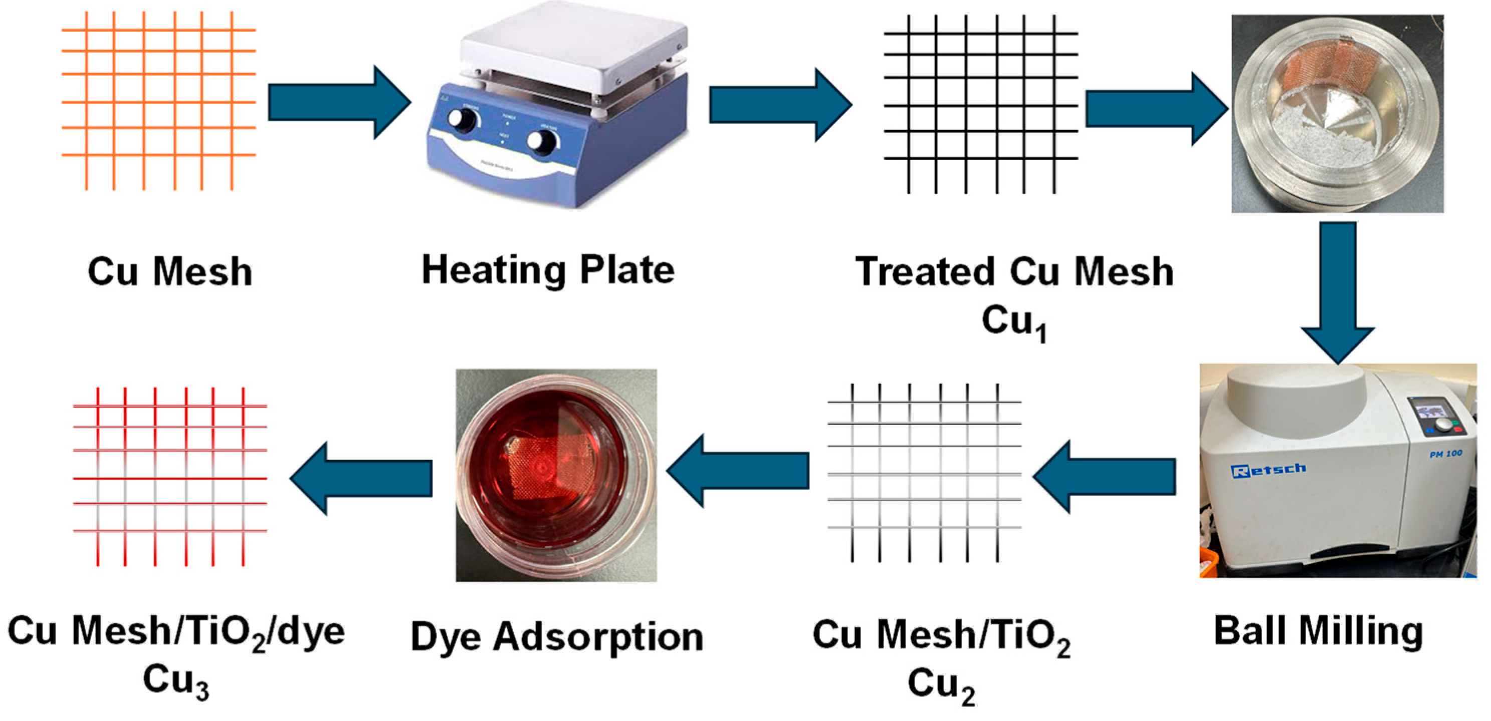
Figure 1. Flowchart outlining the process of fabricating and preparing the electrodes.
Sustainability 17 09478 g001
Figure 2. Experimental setup for testing the photo and electrical response of the fabricated electrodes.
Sustainability 17 09478 g002
Figure 3. SEM images of Cu mesh electrodes showing successful TiO2 deposition at (a) 100 μm and (b) 5 μm. Images are taken a magnification of 15k and beam intensity of 20 kV. The image on the right is the magnified TiO2 layer marked by the red arrows in the image of the left.
Sustainability 17 09478 g003
Figure 4. XRD spectra of Cu mesh electrodes and the anatase TiO2 layer.
Sustainability 17 09478 g004
Figure 5. XPS spectra of the (a) Cu mesh (Cu1), (b) Cu mesh and TiO2 layer (Cu2), and (c) Cu mesh with TiO2 layer and Ru dye loading (Cu3).
Sustainability 17 09478 g005
Figure 6. Raman spectra of the Cu mesh (Cu1), Cu mesh and TiO2 layer (Cu2), and Cu mesh with TiO2 layer and Ru dye loading (Cu3).
Sustainability 17 09478 g006
Figure 7. UV–Vis absorption spectra of the Cu mesh (Cu1), Cu mesh and TiO2 layer (Cu2), Cu mesh with TiO2 layer and Ru dye loading (Cu3), and FTO.
Sustainability 17 09478 g007
Figure 8. Photo response of the Cu mesh (Cu1), Cu mesh and TiO2 layer (Cu2), and Cu mesh with TiO2 layer and Ru dye loading (Cu3).
Sustainability 17 09478 g008
Figure 9. Nyquist plot for Cu mesh (Cu1), Cu mesh and TiO2 layer (Cu2), andCu mesh with TiO2 layer and Ru dye loading (Cu3).
Sustainability 17 09478 g009
Table 1. Summary of the resistance from the Nyquist plot for Cu mesh (Cu1), Cu mesh and TiO2 layer (Cu2), and Cu mesh with TiO2 layer and Ru dye loading (Cu3).
PhotoelectrodeRsRct
Cu190 Ω900 Ω
Cu280 Ω800 Ω
Cu370 Ω380 Ω
Table 2. Bill and cost of materials utilized for the fabrication of the conventional and proposed flexible DSSCs.
Conventional DSSCProposed Flexible DSSC
Electrode Materials
MaterialPrice (AED/unit)Required Quantity (Unit/Batch)MaterialPrice ($/Unit)Required Quantity (Unit/Batch)
FTO340/30 × 30 cm230 cm2Cu mesh54/30 × 100 cm230 cm2
TiO2537/1 kg5 gTiO2537/1 kg2.5 g
PEG60/0.5 L4.5 mL---
Sensitizer and counter electrode materials
MaterialPrice (AED/unit)Required Quantity (unit/batch)
Ruthenium144/200 mg6.84 mg
Ethanol60/2.5 L50 mL
Electrolyte 246/20 mL2 mL
Pt counter electrode246/16 pieces10 pieces
Total Price184 AEDTotal Price172 AED
Table 3. Electricity cost and CO2 emissions associated with the fabrication of conventional and flexible electrodes.
EquipmentProcessPower Rating (kW)Time (min)Energy (kWh)Electricity Cost (AED)CO2 Emission (kg)
Conventional Electrodes
UV-CleanerUV Treatment0.66200.220.0810.18
Hot PlateTiO2 deposition1.05200.350.1290.67
FurnaceTiO2 film annealing4.497.57.152.6455.72
Total Electricity Cost2.864 AEDTotal CO2 Emission6.57 kg
Cu Mesh-based Electrodes
Hot PlateCu mesh treatment1.05300.5250.1940.67
Ball millingTiO2 synthesis and deposition1.25300.6250.2310.50
Total Electricity Cost0.425 AEDTotal CO2 Emission1.17 kg
Table 4. Comparative analysis between conventional, polymer-based, and metallic-based electrodes.
Electrode/CriteriaFTO on GlassPolymer-BasedMetallic-Based
Sheet Resistance7–15 Ω/sq30–500 Ω/sq1–10 Ω/sq
Optical Transmittance80–90%85–95%80–95%
Mechanical FlexibilityPoorExcellentExcellent
Chemical/thermal stabilityExcellent; stable to UV and heatModerate; moisture/UV sensitive, needs encapsulationCu prone to oxidation; TiO2 passivation and encapsulation required
PEC/photo response trendReliable baseline; moderate spikes/plateausFast but lower current density vs. oxides/metalsHighest amplitude and fast transients, good injection via dye → TiO2
Process temperatureHighLowLow
Fabrication complexitySingle thin-film deposition; well-standardizedCoat → mild anneal → (dopants/encapsulation)Facile using ball milling or screen printing
Equipment CAPEXHighLowMedium
Material costModerateLowLow
ScalabilityVery highVery highHigh
Durability in electrolytesHighNeeds barrier layersGood
Recyclability/EHSGlass recyclable; energy-intensive processingMixed (polymer films harder to recycle)Recyclable
SummaryLow risk, proven supply chainLowest CAPEX; great for flexible, low-cost modules but lower conductivity/performance ceilingStrong performance at low material cost (Cu), recyclable, attractive if made via R2R mesh + facile deposition of TiO2
Disclaimer/Publisher’s Note: The statements, opinions and data contained in all publications are solely those of the individual author(s) and contributor(s) and not of MDPI and/or the editor(s). MDPI and/or the editor(s) disclaim responsibility for any injury to people or property resulting from any ideas, methods, instructions or products referred to in the content.