Article

Adaptive Virtual Impedance Control with MPC’s Cost Function for DG Inverters in a Microgrid with Mismatched Feeder Impedances for Future Energy Communities

by
Mubashir Hayat Khan
1,
Shamsul Aizam Zulkifli
2,*,
Nedim Tutkun
3,* and
Alessandro Burgio
4
1
Department of Electrical Engineering, Faculty of Engineering and Technology, University of Poonch Rawalakot, Ghazi e Millat Road-Rawalakot AJ&K, Rawalakot 12350, Pakistan
2
Department of Electrical Engineering, Faculty of Electrical and Electronic Engineering, Universiti Tun Hussein Onn Malaysia, Parit Raja, Batu Pahat 86400, Johor, Malaysia
3
Department of Electrical and Electronics Engineering, Istanbul Ticaret University, 34840 Istanbul, Türkiye
4
Independent Researcher, 87036 Rende, CS, Italy
*
Authors to whom correspondence should be addressed.
Sustainability 2024, 16(2), 525; https://doi.org/10.3390/su16020525
Submission received: 31 October 2023 / Revised: 21 December 2023 / Accepted: 30 December 2023 / Published: 8 January 2024
(This article belongs to the Special Issue Sustainable Electric Power System and Renewable Energy)

Abstract

:
More and more distributed generations (DGs), such as wind, PV or battery bank sources, are connected to electric systems or customer loads. However, the locations of these DGs are based on the highest energy that can be potentially harvested for electric power generation. Therefore, these locations create different line impedances based on the distance from the DGs to the loads or the point of common coupling (PCC). This paper presents an adaptive virtual impedance (AVI) in the predictive control scheme in order to ensure power sharing accuracy and voltage stability at the PCC in a microgrid network. The reference voltage from mismatched feeder impedances was modified by utilizing the suggested AVI-based predictive control for creating equal power sharing between the DGs in order to avoid overburdening any individual DG with low-rated power. The AVI strategy used droop control as the input control for generating equal power sharing, while the AVI output was used as the reference voltage for the finite control set–model predictive control (FCS-MPC) for creating a minimum voltage error deviation for the cost function (CF) for the inverter’s vector switching pattern in order to improve voltage stability at the PCC. The proposed AVI-based controller was tested using two DG inverter circuits in a decentralized control mode with different values of line impedance and rated power. The performance of the suggested controller was compared via MATLAB/Simulink with that of a controller based on static virtual impedance (SVI) in terms of efficiency of power sharing and voltage stability at the PCC. From the results, it was found that (1) the voltage transient magnitude for the AVI-based controller was reduced within less than 0.02 s, and the voltage at the PCC was maintained with about 0.9% error which is the least as compared with those for the SVI-based controller and (2) equal power sharing between the DGs increased during the change in the load demand when using the AVI-based controller as compared with using the SVI-based controller. The proposed controller was capable of giving more accurate power sharing between the DGs, as well as maintaining the voltage at the PCC, which makes it suitable for the power generation of consumer loads based on DG locations for future energy communities.

1. Introduction

Distributed generations (DGs) are capable of providing reliable electric power with a reasonable control ability to meet energy demands. It is apparent that microgrids have higher security and reliability as compared with traditional power grids, such as control flexibility and offering higher power quality to consumers [1]. As microgrids provide several advantages over traditional power grids, researchers have been working on better control mechanisms for different rated values of DGs [2,3,4,5]. It is well known that more renewable energy resources are integrated into power grids to achieve less carbon emissions worldwide.
DG inverter controls in microgrid systems can be categorized as centralized and decentralized controls [6]. In a decentralized control, each DG unit is connected to an inverter that has its own dedicated controller and the feeder line impedance depends on the distance from the DG source to the point of common coupling (PCC). For better power sharing between DGs, the mismatch in feeder line impedances needs to be treated using a control based on the virtual impedance loop, as suggested in [7]. Virtual impedance only needs to be applied in low-voltage microgrids, in which the ratio of reactance to resistance (X/R) or the impedance ratio is usually higher. However, in microgrids with a high impedance ratio, there can be a cross coupling between the active power and reactive power, leading to a power system with an unstable condition [8], which is not suitable for the DG configuration. The basic function of virtual impedance is to manage frequency deviation, voltage stability and load power sharing when there are several DG inverters connected in parallel in a microgrid system [7,9,10]. To design virtual impedance, the rated power capacity and power decoupling for each DG and the power at the PCC are taken into account with inductive and resistive line impedances in the microgrids [11].
Usually, virtual impedance is used in systems with a stationary behavior to extend the transient power regulation due to the systems’ inability to share equal power between the DGs [12]. Virtual impedance in microgrids can be applied for voltage-source converters (VSCs) or current-source converters (CSCs) for power flow control, unbalanced-harmonics compensation and ancillary services, which are needed due to mismatched line impedances [11,13,14]. Generally, DG inverters are based on the VSC model, which is suitable for developing virtual impedance control. Two types of strategies, which are a strategy based on the proportional relation [15,16] and a filter-based strategy using the feedback response of the output filter, have been taken into consideration [17,18]. It is reported in a number of publications that virtual impedance is affected by time delay and control complexity due to the dependency on the structure of virtual impedance and the pulse-width modulation (PWM) switching pattern [14,17] applied in current and voltage control loops in most control schemes [19,20].
Model predictive control (MPC) in power electronic converters has been investigated as an alternative for removing the complex multi-looped-based voltage and current controller, as well as for controlling the flexibility and expandability of the inverter switching operation. MPC, based on the finite control set (FCS), is currently used extensively in inverter control approaches in order to enhance the dynamic performance of systems. As is known, the control technique based on FCS-MPC is implemented without using any external PWM switching, and the inner current-control loop is not necessarily required for output voltage control. Moreover, the FCS-MPC formulation is simple to implement and provides a fast dynamic response when applied in inverter-based microgrids [21,22]. The performance of FCS-MPC for parallel-connected inverters in microgrids in the decentralized control mode using virtual impedance has also been investigated, where a fixed/static virtual impedance (SVI) was added to the system, as suggested in [23,24]. The SVI can ensure power sharing accuracy and voltage compensation at the PCC if the feeder line impedances are equal, but in the case of mismatched line impedances, the accuracy as per connected load/loads is not guaranteed. The voltage deviation in a system with mismatched feeder line impedances with the addition of the SVI keeps increasing when more loads are added [25,26,27].
This paper focuses on the designing of a controller for a DG inverter circuit with mismatched feeder line impedances in order to ensure power sharing accuracy and voltage magnitude compensation at the PCC using the virtual impedance loop with MPC for the generation of switching vectors. The proposed control strategy combines the predictive control scheme with the voltage error algorithm of the MPC’s cost function to create a new reference voltage based on the virtual impedance strategy. Furthermore, the use of adaptive virtual impedance (AVI) is for regulating power sharing between DGs, as well as ensuring voltage stability at the PCC during load changes. The overall control scheme is modeled in the decentralized DG inverter mode in order to avoid miscommunication among the DGs. The controller has two parts, which are the AVI and the FCS-MPC mechanism, in order for it to become an adaptive controller. The contribution of the AVI is to generate the reference voltage based on mismatched line impedances in combination with droop power sharing control as the input for the AVI for high-vector MPC switching to compensate for the fast transience of the voltage at the PCC.
Moreover, it is a dream of authors to see that this controller can be applied in local grid networks. As is known, in the future, an electrical grid network will be localized generation, where energy generation comes from residential energy generation, low-rated solar farm networks, fast-charging stations and portable energy storages that are placed in local communities to create a nano-grid system. This will create continuous and sustainable energy generation and at the same time will increase the awareness of having responsible communities for the environment and will provide a green living condition.
This paper is divided into several sections. Section 1 presents the overview of a microgrid system and control schemes based on the virtual impedance loop, as well as the MPC and issues of power sharing between DGs with different line impedances. In Section 2, the LC filter and inverter voltage control loop based on the transfer function model are referenced for vector control switching. The proposed AVI-based reference voltage for mismatched feeder impedances and the cost function for the MPC’s voltage error generation are given in Section 3 and Section 4, respectively. Section 5 provides the parameter data for the simulation experiment for the DGs used, along with load values and load transition times. The results and discussion are given in Section 6, where the PCC voltage stability and power sharing capability for the AVI-based and SVI-based control schemes are compared for efficiency evaluation. This paper will not discuss the SVI-based controller’s formulation because it has been explained in detail in [15]. This paper ends with the conclusion in Section 7 on whether the proposed controller can be helpful to future energy communities.

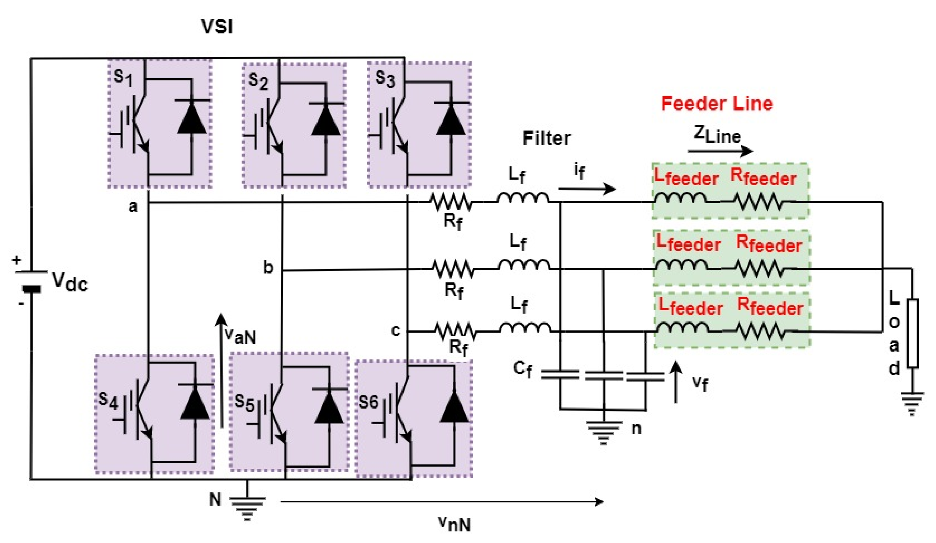
2. LC Filter and Voltage Loop Transfer Function with Switching Voltage Vectors

An LC filter was used to improve the quality of the voltage output, which is a part of the inverter control’s transfer function for the VSC model, as shown in Figure 1 and Figure 2 with the new reference voltage V r e f d q * . The filter voltage’s input and output v i , v o filter and output current i o and i f voltage at the LC filter can be expressed as in the α β transformation to simplify the three-phase circuit to represent a single-circuit diagram:
v o α β = v o α + j v o β = T · v o a b c i f α β = i f α + j i f β = T · i f a b c i o α β = i o α + j i o β = T · i o a b c v i α β = v i α + j v i β = T · v i a b c
From the Clarke transformation, T , i f a b c , i o a b c , v o a b c   and   v i a b c in Equation (1) are expressed as follows:
T = 2 3 [ 1 e j 2 3 π e j 4 3 π ] i f a b c = [ i f a i f b i f c ] , i o a b c = [ i o a i o b i o c ] , v o a b c = [ v o a v o b v o c ] , v i a b c = [ v i a v i b v i c ]
Considering the rate of change of the current and voltage in the α β -reference frame:
d d t ( v o α β ) = 1 C f i f α β 1 C f i o α β
d d t ( i f α β ) = 1 C f ( v i α β ) R f L f ( i f α β ) 1 L f ( v o α β )
where C f   ,   L f are the capacitance and inductance in the filter circuit, respectively. In the state-space form, Equations (2) and (3) are expressed as follows:
d d t [ v o α β i f α β ] = A · [ v f α β i f α β ] + B · [ v i α β i o α β ]
where A and B are given as the following:
A = [ R f L f 1 L f 1 C f 0 ] B = [ 1 L f 0 0 1 C f ]
The inverter voltage can be obtained by subtracting the common voltage from the voltage in each phase, as shown in Equation (5):
V i a b c = [ v i a v i b v i c ] = [ v i a N v i b N v i c N ] v i a N + v i b N + v i c N 3
The inverter voltage in the matrix calculations can be represented as follows:
V i a b c = [ v i a v i b v i c ] = V d c 2 ( I 1 3 .1 ) · S
where I is the identity matrix, 1 is an all-ones matrix and S is the switching action of the inverter.
I = [ 1 0 0 0 1 0 0 0 1 ] , 1 = [ 1 1 1 1 1 1 1 1 1 ]   and   S = [ S a S b S c ]
Here, the inverter input voltage ( v i a b c ) is attained from the switching vectors. The switching arrangements from three gate signals comprise “0” and “1” to produce (2)3 switching signals as the output of the inverter voltage [25] for the generation of the switching pattern, given as follows:
Sa = “0” when S1 is off and S4 is on, and “1” when S1 is on and S4 is off
Sb = “0” when S2 is off and S5 is on, and “1” when S2 is on and S5 is off
Sc = “0” when S3 is off and S6 is on, and “1” when S3 is on and S6 is off
The product of S a , S b , S c and v d c (DC source voltage) with respect to point N computes the values for v a N , v b N and v c N , as given below:
v a N = S a · v d c v b N = S b · v d c v c N = S c · v d c
The output voltage vector is obtained from the consideration of unitary vector “a”, which also characterizes a phase shift of 120° between phases. Vector “a” is defined as follows:
a = e j 2 π / 3 = 1 / 2 + j 3 2
So, the output voltage can be calculated as follows:
v = 2 ( v a N + a · v b N + a 2 · v c N ) 3
where v a N , v b N , v c N are phase-to-neutral voltages that are associated with the inverter. 
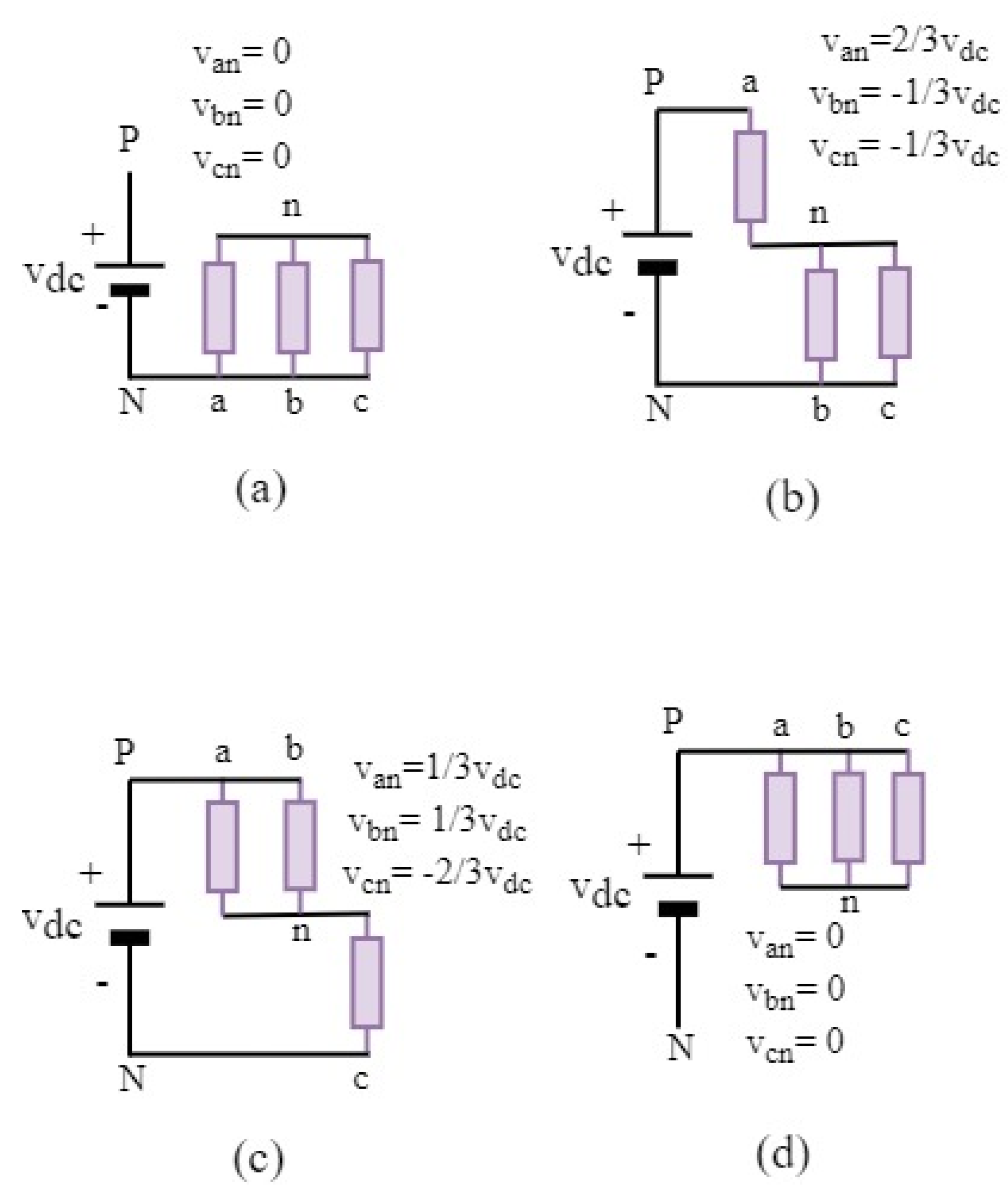
Figure 1 shows the inverter voltage with switching.
From ( S a , S b , S c ) , the voltage vector is generated. For ( S a , S b , S c ) = ( 0 , 0 , 0 ) , the voltage vector V 0 is generated. Computing the values of ( S a , S b , S c ) , the voltage vector is calculated as follows:
V 0 = 2 ( 0 + a .0 + a 2 .0 ) 3 = 0
Similarly, for V 1 , taking ( S a , S b , S c ) = ( 1 , 0 , 0 ) , the voltage vector is calculated as follows:
V 1 = 2 ( v d c + a .0 + a 2 .0 ) 3 = 2 3 v d c
For V 2 , taking ( S a , S b , S c ) = ( 1 , 1 , 0 ) , the voltage vector is calculated as follows:
V 2 = 2 ( v d c + a · v d c + a 2 .0 ) 3 = 2 3 ( v d c + ( 1 2 + j 3 2 ) v d c ) + a 2 .0 = v d c 3 + j 3 2 v d c
So, for all possible number of switching states, which is 2 3 = 8 , all voltage vectors are calculated. It is worth mentioning here that V 0 = V 7 for switching states ( S a , S b , S c ) = ( 0 , 0 , 0 )   and   ( 1 , 1 , 1 ) . The finite sets of seven different voltage vectors are obtained from the switching states, which are given in Table 1:
The state-space model of the LC filter given in Equation (4) is converted into discrete time by using the zero-order hold (ZOH) [26] for discrete sampling for the vector pattern. Equation (8) is the discrete-time representation of Equation (4):
[ i f α β v o α β ] = A d [ i f α β v o α β ] + B d [ v i α β i o α β ]
where A d = e A T s , B d = 0 T s e A τ · B d τ and T s is the sampling time of 12 × 10−6. The switching sequence generates the signal for the inverter, which will be utilized in the FCS-MPC vector control operation.

3. Modeling of Adaptive Virtual Impedance (AVI) in a System with Mismatched Feeder Impedances

The resistance, inductance and capacitance values for the line impedance were calculated as 0.1 Ω, 3.3 mH and 20 μF, respectively. For the inverter switching operation, the switching frequency (fsw) was 20 kHz, while the cut-off frequency (fCF) of the LC filter was 2 kHz, based on 10% switching from the switching frequency selected. The P and Q control in the conventional droop theory employed the power control input for the AVI, which was based on the decentralized inverter control. The voltage and frequency droop equations are given as follows:
V r e f = V n o m m p ( P i P r e f )
ω r e f = ω n o m + n q ( Q i Q r e f )
For an islanded microgrid, the reference active power and reference reactive power (Pref and Qref) are taken as 0 for power sharing accuracy. Therefore, Equations (9) and (10) can be written as follows:
V r e f = V n o m m p P i
ω r e f = ω n o m + n q Q i
In Equations (11) and (12), m p   and   n q are droop coefficients. As explained earlier, the parallel inverters, the conventional droop control and the voltage should correspond to any changes in P and Q to change V and f at the PCC. So, the proposed AVI should compensate for power changes at the PCC when the load changes. Therefore, the reference voltage in the dq-reference frame is modified as follows:
[ V d q ] = [ ( k p v · ( V n o m V o d q ) + k i v 0 t ( V n o m V o d q ) d τ ) ] · [ V r e f d q ] [ V d q ] = [ ( k p v · ( V n o m V o d q ) + k i v 0 t ( V n o m V o d q ) d τ ) ] · [ ( V n o m m p P i ) ]
In Equation (13), k p v and k i v are PI controller gains and V d q is the reference voltage for the dq-reference frame obtained from the conventional droop control for controlling P and Q based on the change in V and F. For the SVI-based control, the modified reference voltage should be combined with the SVI, given as follows:
V v i r = V r e f ( R S V I ) i o
In the case of mismatched feeder impedances, the SVI-based control is not sufficient. Therefore, a droop-based AVI control was implemented to give more robustness to the DGs during mismatched line impedances. Equation (14) can be modified and expressed with virtual impedance as follows:
[ V A V I d q ] = [ R v i r ω n o m L v i r ω n o m L v i r R v i r ] · [ i o d q ]
The output of the AVI will generate a new reference voltage for the cost function input for the MPC, which will be explained in Section 4. This reference voltage can be further modified with the droop reference voltage and virtual impedance, and the new equation is expressed as follows:
[ V A V I d q ] = [ [ ( k p v · ( V n o m V o d q ) + k i v 0 t ( V n o m V o d q ) d τ ) ] · [ V r e f _ d r o o p d q ] ] + [ ( R v i r + R f e e d e r ) ( ω n o m ( L v i r + L f e e d e r ) ) ( ω n o m ( L v i r + L f e e d e r ) ) ( R v i r + R f e e d e r ) ] · [ i o d q ]
Therefore, AVI inputs are still used in the droop equation, where power can be shared between parallel-connected DGs based on P and Q at the PCC. The simplified reference voltage in the dq-reference frame from the AVI output is given in Equation (17):
[ V r e f d q * ] = [ [ ( k p v · ( V n o m V o d q ) + k i v 0 t ( V n o m V o d q ) d τ ) ] · [ ( V n o m m p P i ) ] ] + [ [ k p L · ( Q t Q ) + k i L 0 t ( Q t Q )   d τ ] · [ ( R v i r + R f e e d e r ) ω n o m ( L v i r + L f e e d e r ) ω n o m ( L v i r + L f e e d e r ) ( R v i r + R f e e d e r ) ] · [ i o d q ] ]
where k p L   and   k i L are PI controller gains for the AVI, which are used for equal power sharing. As given in Equation (13), the modified reference voltage V r e f d q * is obtained through the AVI control mechanism’s output with the integration of virtual line impedance and droop control in the mathematical control model. Parameter Q t is the measured reactive power connected in parallel at the PCC. Equation (17) is the generated reference voltage for the next FSC-MPC process, which will be discussed in the next section, for the cost function’s error quantification. Figure 2 shows the block diagram of the control structure of the AVI-based control and SVI-based control via the virtual impedance strategy for the reference voltage input for the MPC, along with relevant equations used for the controller’s functions.
As a recap, in the SVI-based control technique, load power sharing as per the connected load is not accurate, and voltage deviations occur at the PCC in systems with mismatched line impedances. A fixed value of virtual impedance is needed to mitigate the line impedance mismatch and is applied to the predefined line impedance. The virtual impedance with a fixed value is added to a system with mismatched line impedances to balance the inequality. The integration of the AVI-based control with the predictive cost function as the MPC input is explained in Section 4.
Table 2 shows the difference between the proposed AVI-based and existing SVI-based control techniques. As concluded from the table, in the SVI-based control, the shared power by each DG inverter is not accurate as per the connected load, because the static virtual impedance does not adjust itself to the change in the line impedance value. Moreover, there are voltage deviations due to the addition of static virtual impedance, where the voltage keeps on deviating with additional loads in a system with mismatched feeder impedances.

4. Modeling Predictive Cost Function for FCS-MPC’s Vector Control

The cost function is the most essential parameter for the MPC-based control technique, as it generates the vector control for the inverter’s switching pattern. Predictions are made on the receding horizon pattern at k + 2 steps [27] in the α β reference frame, formulated as follows:
J 1 = | V r e f α β [ k + 2 ] | | v o α β [ k + 2 ] | 2
where V r e f α β   and   v o α β are the reference voltage and output voltage to the inverter, respectively. Parameter V r e f α β   is tracked by v o α β at two steps ahead (k + 2) at a sampling time (Ts) of 12 × 10−6 in the finite control set (FCS).
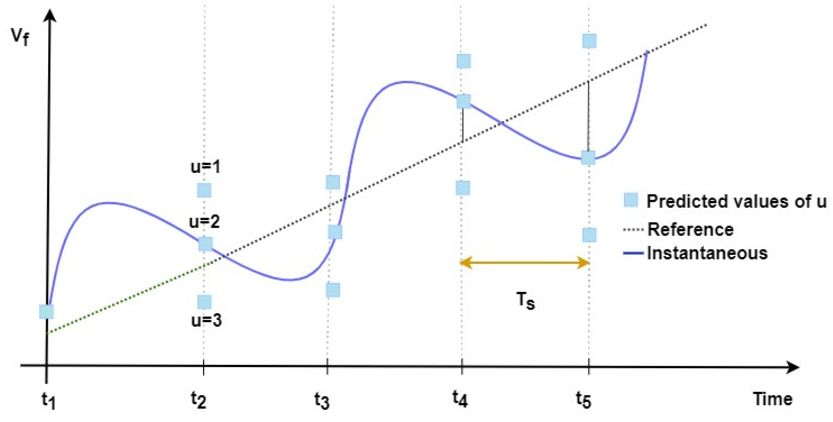
In the conventional FCS-MPC, the cost function (CF) is implemented in first-order systems, which is determined by the node circuit equation of the inverter, as second-order or higher-order systems with a CF show an unstable behavior. In first-order systems, there is no cross coupling between impedances, while in higher-order systems, there is a cross-coupling equation among the state variables. Also, in first-order systems, the capacitor’s voltage is directly regulated by the filter’s current. However, in second- or higher-order systems, the capacitor’s voltage is indirectly regulated by the current of the inductor in the inverter. Therefore, the voltage tracking error continuously increases, as shown in Figure 3, where the predicted trajectory is heading away from the reference (dotted line) at any particular time interval. So, the CF in Equation (18) for the FCS is needed to track the reference voltage and to give small derivative terms simultaneously in order to minimize the tracking error effect between the reference and actual loop feedback.
Therefore, voltage derivative terms should be taken into account from the inductor’s current in order to regulate the capacitor’s voltage in the filter circuit. The reference voltage obtained from the AVI is the derivative function for the CF, expressed as follows:
d d t ( v r e f ( t ) ) = ω r e f V r e f · cos ( ω r e f t ) j ω r e f V r e f · sin ( ω r e f t )
d v o α β ( t ) d t = 1 C f ( i f α ( t ) i o α ( t ) ) + j 1 C f ( i f β ( t ) i o β ( t ) )
where ω r e f V r e f · cos ( ω r e f t ) = ω r e f v r e f β ( t ) and ω r e f V r e f · sin ( ω r e f t ) = ω r e f v r e f α ( t ) . The capacitor’s voltage is represented by v o α β . Next, by taking the derivatives of the reference voltage and output voltage of the AVI-based control with the step CF, the combination is formulated as follows:
J A V I = ( C f · ω r e f · v r e f α ( k + 2 ) ) i f α ( k + 2 ) + i o α ( k + 2 ) ) 2 + ( C f · ω r e f 1 · v r e f β ( k + 2 ) ) i f β ( k + 2 ) + i o β ( k + 2 ) ) 2
Based on Equation (21), the reference voltage v r e f is attained from the AVI output, as explained in Section 3, and this v r e f is proportional to the CF. Here, J A V I is with a two-step-ahead prediction (k + 2). Therefore, the CF formula in Equation (21) is combined with the AVI output’s reference voltage to generate the CF-minimized error, computed as follows:
J F = [ ( V r e f α [ k + 2 ] v o α [ k + 2 ] ) + ( V r e f β [ k + 2 ] v o β [ k + 2 ] ) 2 ] + λ d ( ( C f · ω r e f · v r e f α ( k + 2 ) i f α ( k + 2 ) + i o α ( k + 2 ) ) 2 + ( C f · ω r e f · v r e f β ( k + 2 ) i f β ( k + 2 ) + i o β ( k + 2 ) ) 2 ) + ( h lim + λ u s w 2 )
where λ u   and   λ d are weighting factors to address the uncertainties in the system.
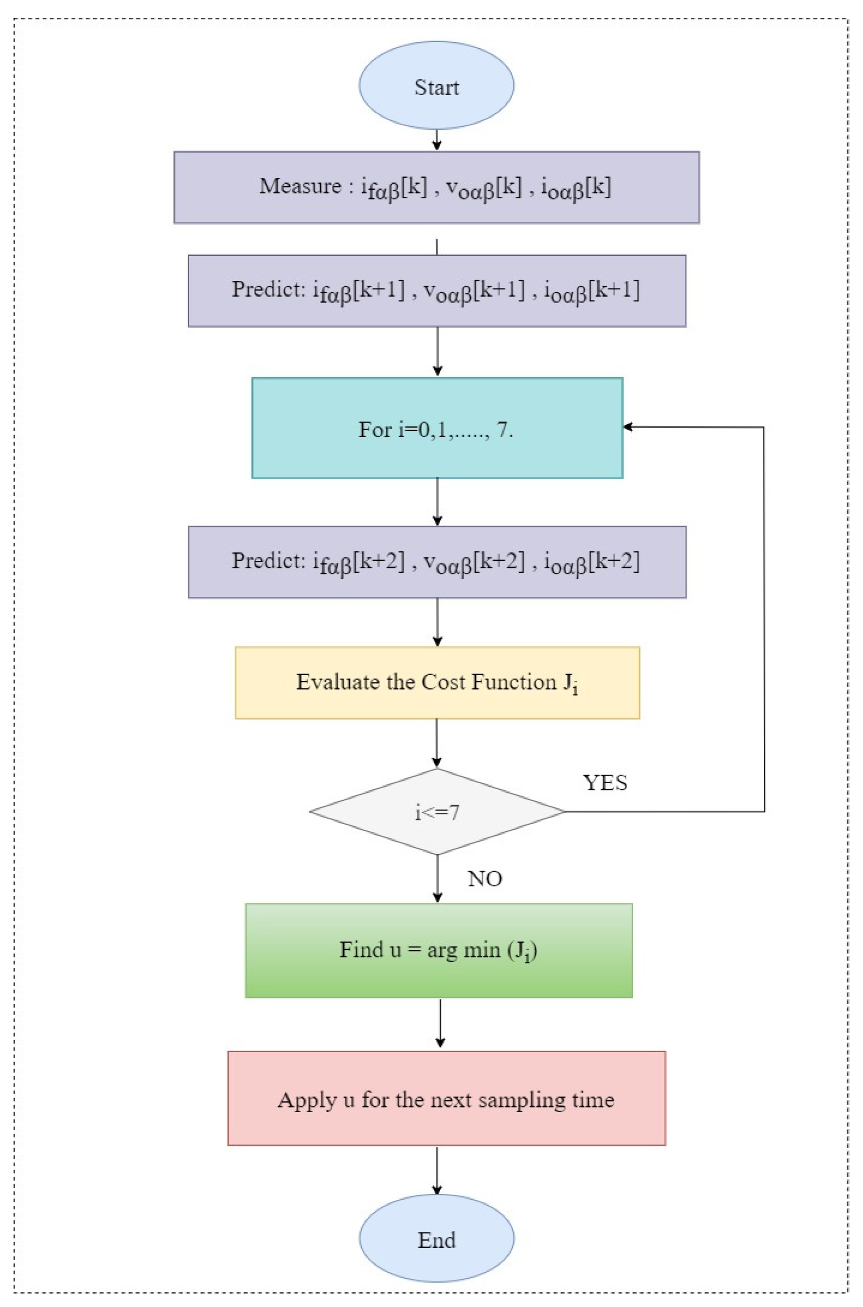
For the SVI-based control scheme, the cost function is calculated using the reference voltage given in Equation (14), whereas the updated reference voltage in Equation (22) is used for the cost function calculation for the proposed FCS-MPC scheme. The flow chart of the control algorithms of the cost function for the proposed FCS-MPC controller is shown in Figure 4.
Figure 5 shows the block diagram of AVI-FCS-MPC and SVI-FCS-MPC with the addition of Equation (22) for the AVI-based control and Equation (14) for the SVI-based control for the minimization of the CF for the transient response of the VSC control in the inverter with the reference voltage V r e f d q * . The weighting factor is obtained through the trial-and-error method from 0 to 0.1 while tuning the controller. Hence, h lim ( i ) = 0 when i f ( i ) i max , and h lim ( i ) = when i f ( i ) > i max , s w ( i ) = ( u ( i ) u ( i 1 ) ) .

5. Islanded Microgrid Block Circuit Simulation and System Parameters for DG Inverters

The AVI-based FCS-MPC was tested individually in the decentralized mode for parallel DG inverters connected to the PCC with different line impedances, as shown in Figure 5 in Section 4. The load was represented by four different load ratings connected at the PCC at specific times, as given in Table 3. This was to create load changes at the PCC in order to check for the robustness of the proposed AVI-based controller. The AVI-MPC controller’s performance was compared with that of the conventional SVI-based controller in [15]. Figure 4 illustrates the simulation test system modeled in MATLAB/Simulink for determining the effectiveness of the AVI-based and SVI-based control models. The simulated microgrid system was tested with two different-rated DGs, as well as different LC filters, different feeder lines and variable loads, as shown in Figure 6.

6. Results and Discussion

In this section, the results for the AVI-MPC and SVI-based control are shown and discussed. The real and reactive power sharing, the voltage at the PCC, the current to the load and the frequency deviation during load changes were measured for each DG inverter. As for the load, Load1 was connected from 0 s to 1 s at 1.2 kW, Load2 from 1 s to 2 s at 0.5 kW, Load3 from 2 s to 3 s at 0.7 kW and, finally, Load4 from 3 s to 4 s at 1 kW. The aim was to show the reliability of the suggested AVI-based controller, where equal power sharing between the DGs, as well as voltage stability could be achieved. The percentage error for the voltage and current is calculated as follows:
P e r c e n t a g e   v o l t a g e   e r r o r   a t   P C C = V o l t a g e / C u r r e n t   m a g n i t u d e   m e a s u r e d   a t   P C C T a r g e t N o m i n a l V o l t a g e   m a g n i t u d e × 100 %
The percentage error for power sharing accuracy in the result section is calculated as follows:
P e r c e n t a g e   p o w e r   s h a r i n g   e r r o r   a t   P C C = L o a d   p o w e r   s h a r e d   b y   e a c h   D G   i n v e r t e r   a t   P C C L o a d   c o n n e c t e d   t o   t h e   s y s t e m × 100 %
  • PCC Voltage During Load Changes (Low to High and Vice Versa)
The voltage output at the PCC is shown and explained in this subsection. The performance of the suggested AVI-MPC was compared with that of the SVI-based control. 
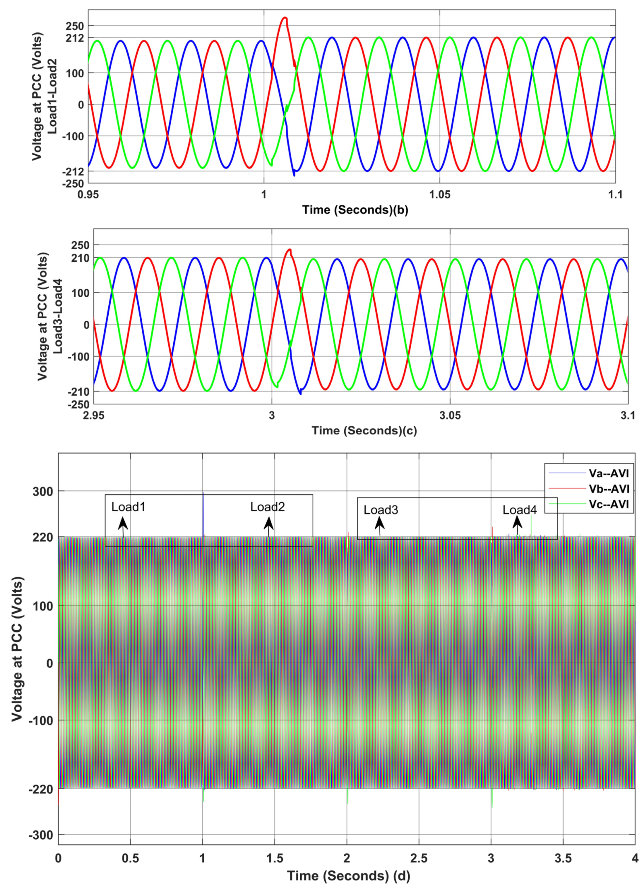
Figure 7a shows the voltage profile at the PCC when load transitions were applied for the SVI-based controller. As shown in the zoomed-in images in Figure 7b,c, the voltages at the PCC when Load1, Load2, Load3 and Load4 were connected were 206 V, 212 V, 210 V and 205.5 V, respectively, which were not at the rated PCC voltages.
Figure 7d shows the voltage magnitudes at the PCC for the proposed AVI-MPC, where the PCC voltage was near the rated values stated in Table 4. The zoomed-in image in Figure 7e shows that the voltage at the PCC was 218 V when Load1 was connected, and it was still maintained at 219.5 V when Load2 was connected. Figure 7f shows the zoomed-in image of the voltage profile when Load3 and Load4 were connected, where the voltage at the PCC still remained at 220 V. Table 4 shows the comparison of the percentage errors of the voltages at the PCC for the controllers. It is clear from this result that the proposed AVI-based predictive control scheme successfully maintained the voltage magnitude at the PCC at 220 V with minimum errors.
B.
Current Output During Load Changes (Low to High and Vice Versa)
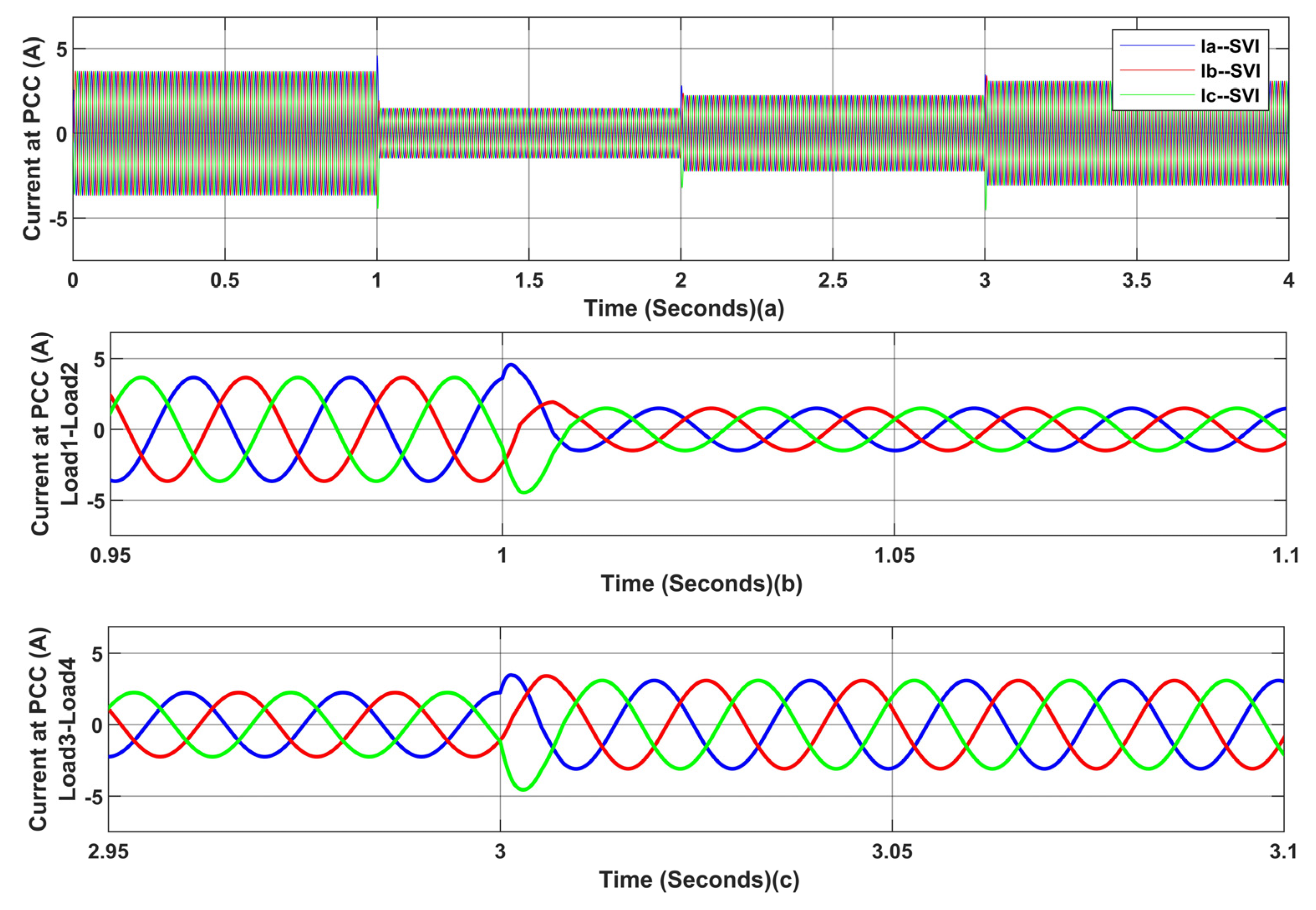
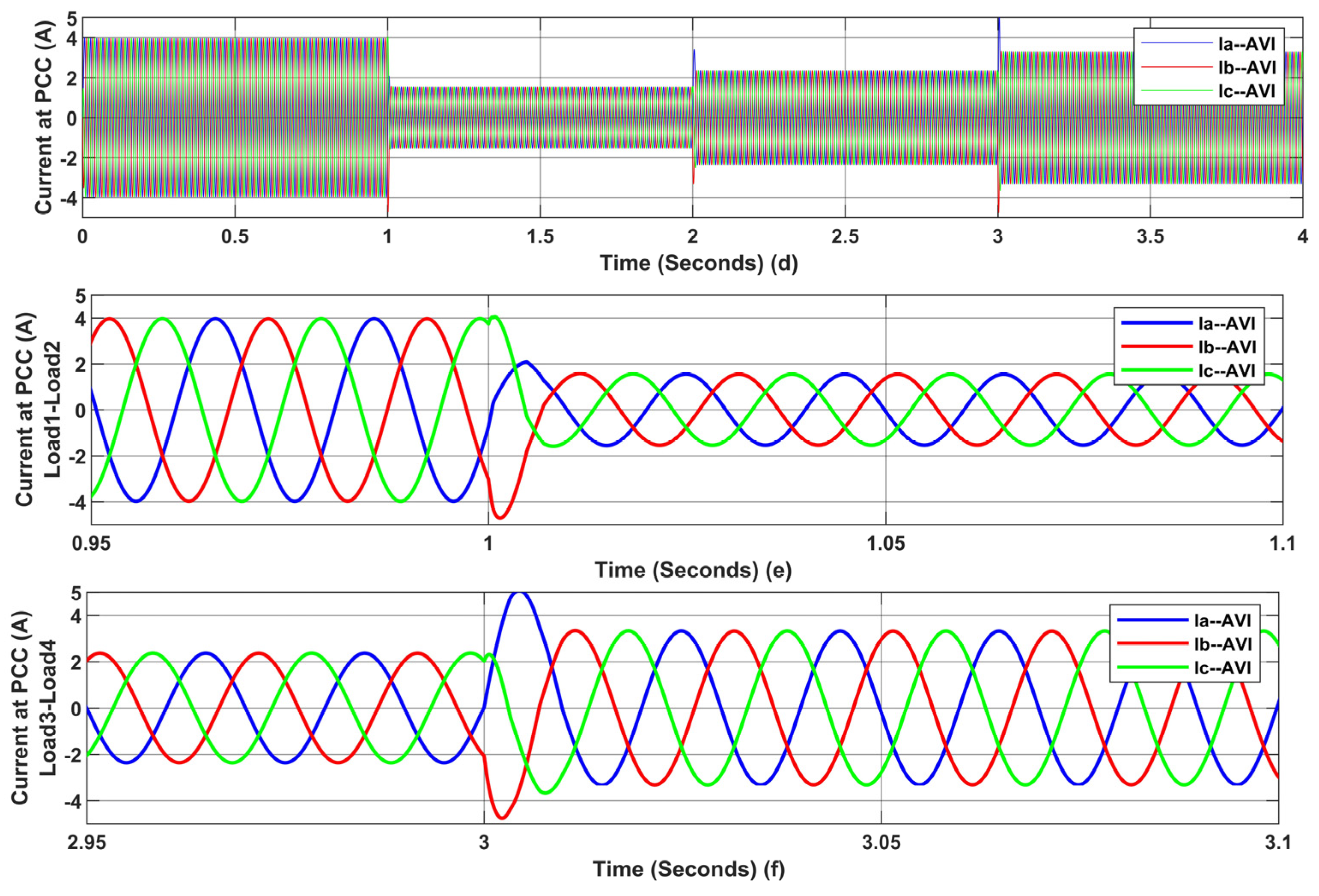
The current outputs at the PCC during load transience from high to low loads and vice versa were also compared and analyzed. Figure 8a–c show the output current result at the PCC when the DGs were operated using the SVI-based controller. The zoomed-in images in Figure 8b,c show increased transient responses when the rated load value changed from high to low and from low to high, where current outputs were measured at 3.94 A, 1.54 A, 2.61 A and 3.4 A when Load1, Load2, Load3 and Load4 were connected, respectively.
Figure 8d–f show the output current when the proposed AVI-based predictive controller was used. The zoomed-in images in Figure 8e,f show that there was no transient effect on the current when the load changed, as based on the time stated in Table 3. In general, if the transient current is more than the rated current, the circuit breaker will be activated, and it will cause DGs to disconnect from the PCC. Moreover, the output currents, which were measured at 3.97 A, 1.54 A, 2.36 A and 3.3 A when Load1, Load2, Load3 and Load4 were connected, respectively, were at the allowable rated value, and, hence, minimum transience was obtained using the AVI-based controller.
C.
Active and Reactive Power Sharing Between DGs During Load Transitions
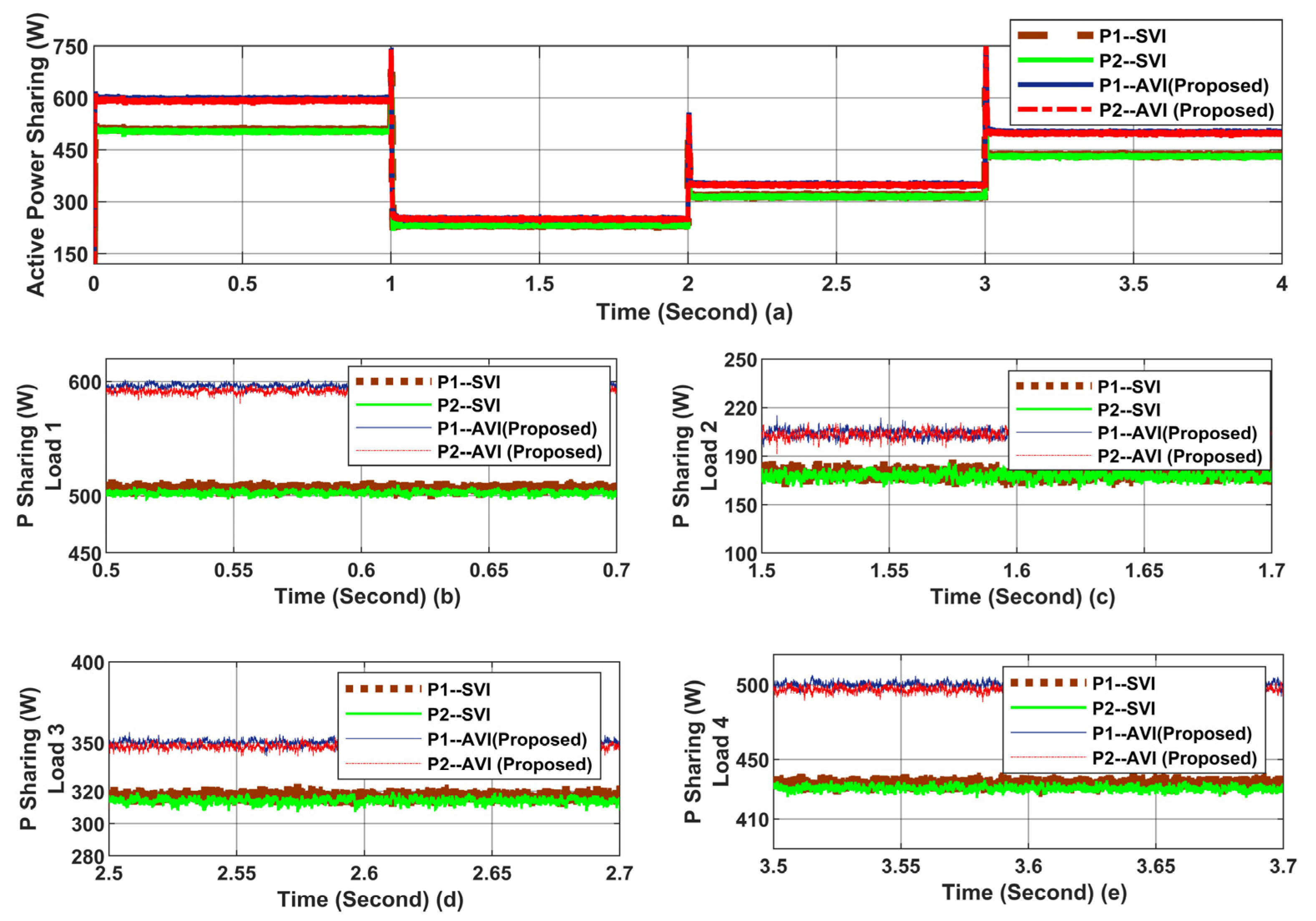
The active power sharing between DG1 and DG2 for the SVI-based control scheme and the proposed AVI-MPC scheme is discussed in this subsection. The power sharing values between DG1 and DG2 for the controllers when Load1, Load2, Load3 and Load4 were connected at different time intervals are shown in Figure 9a. For the SVI-based controller, DG1 and DG2 shared 500 W when Load1 was connected at the PCC, 240 W when Load2 was connected, 318 W when Load3 was connected and 445 W when Load4 was connected, but the DGs should generate about 1200 W, 500 W, 700 W and 1000 W, respectively, based on Table 2. Although DG1 and DG2 shared equal power, this power sharing was not enough as needed by the load, which caused mismatched power generation by the DGs. For the AVI-based controller, the power shared between DG1 and DG2 when Load1 was connected at the PCC was 597.5 W, which totaled to about 1.2 kW, nearly the same as that tabulated in Table 2.
The power sharing between DG1 and DG2 for the SVI-based and AVI-based controllers when Load1 was connected is shown in Figure 9b, where the AVI-based controller was able to have equal power sharing at 600 W for each DG when Load1 required 1.2 kW. Figure 9c–e show similar results on the quality of active power sharing between the DGs for the AVI-based and SVI-based controllers. The AVI-based controller showed a more accurate sharing capability, where it can reach the rated value of Load2. Therefore, the obtained results indicate that the proposed controller was more capable of sharing equal and accurate active power than the AVI-based controller. This is because the reference input to the AVI started with the calculations of P and Q needed by the load.
Figure 10 shows the comparison of the total load active power received at the PCC for the SVI-based controller and the proposed AVI-based controller in order for the controllers to supply the rated load power when a load was connected at the PCC. The load transitions are shown in Figure 10a for Load1, Load2, Load3 and Load4. For the SVI-based controller, the values of the total active power were 1000 W, 480 W, 636 W and 890 W when Load1, Load2, Load3 and Load4 were connected, respectively, which did not achieve the rated load values stated in Table 2. However, for the AVI-based controller, all the required load values were achieved when Load1, Load2, Load3 and Load4 were connected, which were 1195 W, 499.5 W, 698 W and 996.5 W, as shown in Figure 10b–e, respectively. Therefore, the results show that the AVI-based predictive controller was capable of supplying the rated power needed by the load from the DGs in order to avoid excessive power-loss dissipation at the PCC. Table 5 shows the comparison of the active power sharing between the DGs and the load active power at the PCC for the SVI-based and AVI-based control schemes, along with power error percentages.
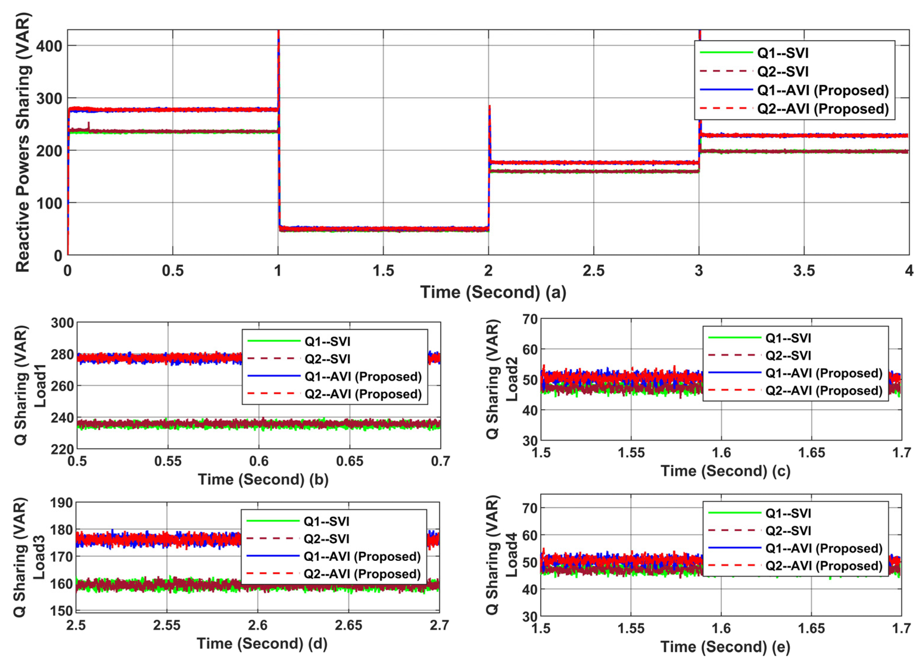
The results of the reactive power sharing for the SVI-based controller and AVI-based controller are shown in Figure 11a. The results show that the shared power, when using the AVI-based controller, was close to the rated Q needed by the load during load changes. The zoomed-in images in Figure 11b–e give a clear visualization of when the SVI-based and AVI-based controllers were used. When Load1 was connected, as shown in Figure 11b, the reactive power shared by each DG inverter was 273.5 Var for the AVI-based controller, which was higher than the reactive power shared at 248 Var for the SVI-based controller. However, when the low-rated loads of Load2 and Load3 were connected, the reactive power sharing values between the DGs for both controllers were almost the same, as shown in Figure 11c–e. This shows that if the Var required by the load was low, the DGs in both controllers can share the Q evenly but not when a high Q value was needed by the load for the SVI-based controller.
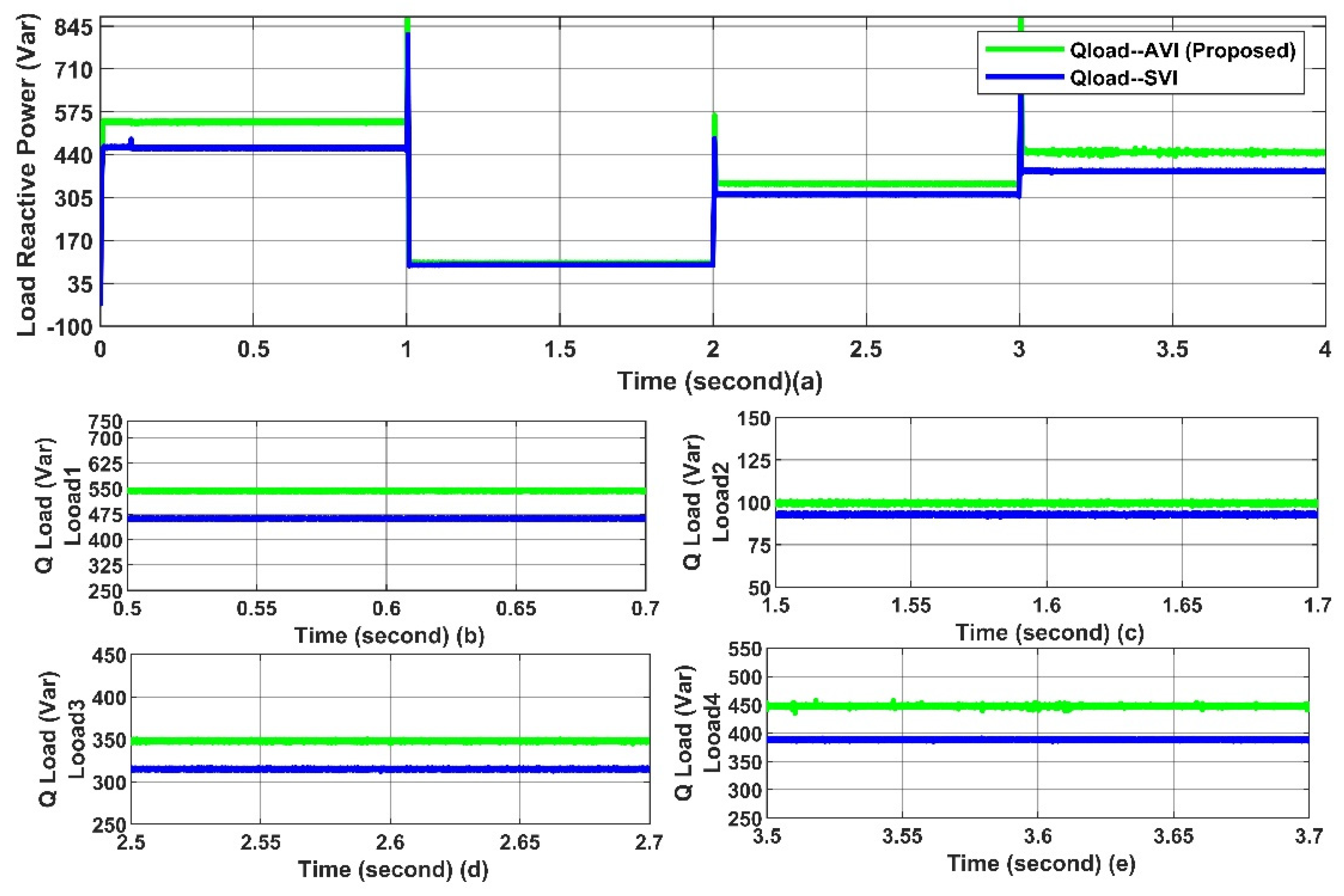
The results of the load reactive power at the PCC for the SVI-based and AVI-based controllers are shown in Figure 12a, and the zoomed-in images of the load reactive power during each load transition are shown in Figure 12b–e. In the case of the SVI-based controller, the reactive powers supplied by each DG to Load1, Load2, Load3 and Load4 were 480 Var, 90 Var, 320 Var and 394 Var, respectively. However, for the AVI-based controller, the total reactive powers when Load1, Load2, Load3 and Load4 were connected were 547 Var, 100 Var, 350 Var and 450 Var, respectively, which were similar to the values specified in Table 2 for the loads. A comparison provided in Table 6 shows the difference between the performances of the two controllers in terms of real and active power sharing, which highlights the contribution of the AVI and its accuracy based on percentage errors.
D.
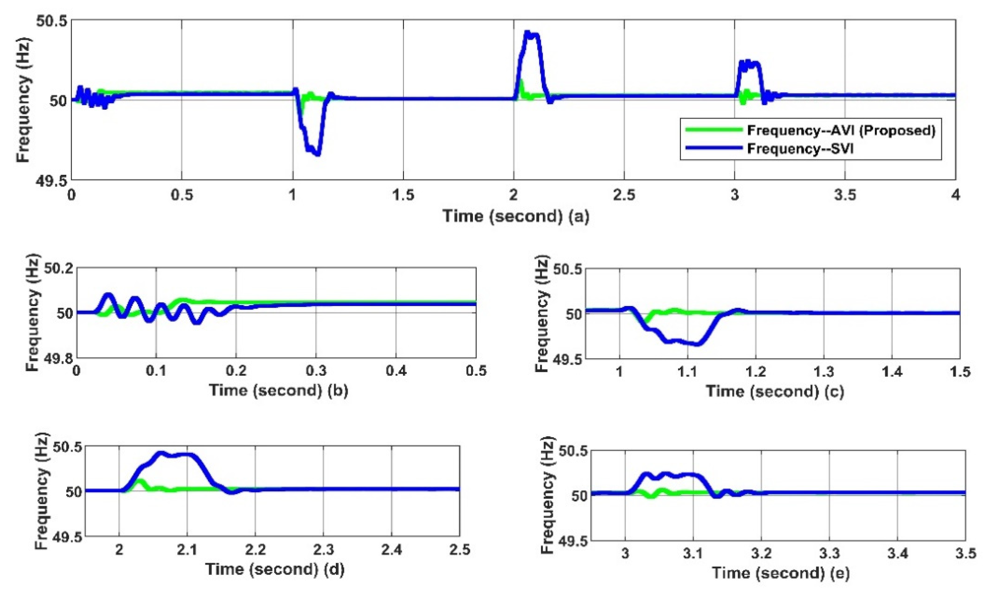
Frequency Response During Load Changes (Low to High and Vice Versa)
The PCC frequency response was also a very important parameter to be checked in order to avoid frequency deviation during the synchronization of DG inverters with the load. The frequency deviation was caused by the load changes, and this deviation should range between 49 Hz to 51 Hz to avoid a frequency swing in the microgrid. A minimized deviation would indicate that the controller was working efficiently in terms of its response at the transient time. The frequency response comparison is shown in Figure 13a–e for the SVI-based and AVI-MPC control schemes. When the SVI-based controller was applied to the DG inverters, the frequency responses at the PCC were approximately 50.4 Hz, 50.01 Hz, 50.02 Hz and 50.035 Hz when Load1, Load2, Load3 and Load4 were connected, respectively, as shown in Figure 13a–e. However, with the proposed AVI-based control, the frequency responses when Load1, Load2, Load3 and Load4 were connected were approximately 50.038 Hz, 50 Hz, 50.1 Hz and 50.03 Hz, respectively, which shows a more stable result. Moreover, both the SVI-based and AVI-based controllers were able to limit the deviations to within the allowable limit, which proved that the proposed controllers were able to regulate the frequency response, as shown in Figure 13a–e.

7. Conclusions

An AVI-based predictive controller is proposed and presented in this paper, and it has shown the ability of equal power sharing whenever the line impedance values of the DG inverters were different, and it maintains the voltage at the PCC. The “adaptive” concept for the proposed controller is due to the inputs of the AVI being based on the droop control of P and Q deviations at the PCC because of load changes. It was necessary to have small deviations in order to provide equal power sharing between DGs. As a result, the AVI generated the reference voltage with a minimum error as the input for the FCS-MPC with a consideration of the CF’s error trajectory. It created a reference voltage for inverter switching with a two-step-ahead prediction (k + 2) at the sampling time (Ts) for 0 to 7 vector coordinates. All the results show that the voltage at the PCC was maintained successfully when load changes were applied at the PCC. In addition, the proposed AVI-based predictive control was able to increase the active and reactive power sharing between the DGs and was able to achieve the required load power at the rated power when measured at the PCC. The time transient effectiveness during load changes for the AVI-based controller with FSC-MPC proved its faster tracking capability. Lastly, all the results indicate that the proposed AVI-based controller has the capability to be used in the DG inverter operation, where it can maximize the power generation at the PCC and create equal power sharing among the DGs. At the same time, it can also be applied in future energy generation such as in hybrid-energy sources’ generation for mitigating circulating currents due to mismatched line impedances. Furthermore, the proposed control scheme can also be applied in local grid networks for future local energy generation at the communities’ areas, which is known as the nano-grid network.

Author Contributions

Conceptualization, M.H.K. and S.A.Z.; methodology, M.H.K. and S.A.Z.; software, M.H.K.; validation, S.A.Z., N.T. and A.B.; formal analysis, M.H.K.; investigation, M.H.K. and S.A.Z.; resources, M.H.K. and S.A.Z.; data curation, M.H.K., S.A.Z., N.T. and A.B.; writing—original draft preparation, M.H.K.; writing—review and editing, S.A.Z., N.T. and A.B.; visualization, M.H.K.; supervision, S.A.Z.; project administration, S.A.Z., N.T. and A.B.; funding acquisition, N.T. and A.B. All authors have read and agreed to the published version of the manuscript.

Funding

This research received no external funding.

Institutional Review Board Statement

Not applicable.

Informed Consent Statement

Not applicable.

Data Availability Statement

Data is contained within the article.

Acknowledgments

The authors would like to express their gratitude to everyone who contributed to this research work. This research was supported by Universiti Tun Hussein Onn Malaysia (UTHM) and the Department of Electrical and Electronics, Ticaret University, Istanbul, Turkey. In addition, the authors would like to express their gratitude to the group members, especially to Momoh Kabir from Advanced Control on Power Converters (ACPC), the Faculty of Electrical and Electronic Engineering, UTHM, for assisting in the administrative work of this research.

Conflicts of Interest

The authors declare no conflict of interest.

References

  1. Shahgholian, G. A brief review on microgrids: Operation, applications, modeling, and control. Int. Trans. Electr. Energy Syst. 2021, 31, e12885. [Google Scholar] [CrossRef]
  2. Hernández-Mayoral, E.; Madrigal-Martínez, M.; Mina-Antonio, J.D.; Iracheta-Cortez, R.; Enríquez-Santiago, J.A.; Rodríguez-Rivera, O.; Martínez-Reyes, G.; Mendoza-Santos, E. A Comprehensive Review on Power-Quality Issues, Optimization Techniques, and Control Strategies of Microgrid Based on Renewable Energy Sources. Sustainability 2023, 15, 9847. [Google Scholar] [CrossRef]
  3. Hmad, J.; Houari, A.; Bouzid, A.E.M.; Saim, A.; Trabelsi, H. A Review on Mode Transition Strategies between Grid-Connected and Standalone Operation of Voltage Source Inverters-Based Microgrids. Energies 2023, 16, 5062. [Google Scholar] [CrossRef]
  4. Jiang, Y.; Yang, Y.; Tan, S.C.; Hui, S.Y.R. Power loss mitigation of parallel-connected distributed energy resources in DC microgrids using a distributed gradient algorithm-based hierarchical control. IEEE Trans. Smart Grid 2022, 13, 4538–4550. [Google Scholar] [CrossRef]
  5. Jiang, Y.; Yang, Y.; Tan, S.-C.; Hui, S.-Y.R. Distribution power loss mitigation of parallel-connected distributed energy resources in low-voltage dc microgrids using a lagrange multiplier-based adaptive droop control. IEEE Trans. Power Electron. 2021, 36, 9105–9118. [Google Scholar] [CrossRef]
  6. Abbasi, M.; Abbasi, E.; Li, L.; Aguilera, R.P.; Lu, D.; Wang, F. Review on the Microgrid Concept, Structures, Components, Communication Systems, and Control Methods. Energies 2023, 16, 484. [Google Scholar] [CrossRef]
  7. Han, Y.; Li, H.; Shen, P.; Coelho, E.A.A.; Guerrero, J.M. Review of Active and Reactive Power Sharing Strategies in Hierarchical Controlled Microgrids. IEEE Trans. Power Electron. 2017, 32, 2427–2451. [Google Scholar] [CrossRef]
  8. Mohammed, N.; Lashab, A.; Ciobotaru, M.; Guerrero, J.M. Accurate Reactive Power Sharing Strategy for Droop-Based Islanded AC Microgrids. IEEE Trans. Ind. Electron. 2022, 70, 2696–2707. [Google Scholar] [CrossRef]
  9. Mohammed, N.; Ciobotaru, M. An Accurate Reactive Power Sharing Strategy for an Islanded Microgrid Based on Online Feeder Impedance Estimation. In Proceedings of the IECON 2020 The 46th Annual Conference of the IEEE Industrial Electronics Society, Singapore, 18–21 October 2020; pp. 2525–2530. [Google Scholar]
  10. Bai, X.; Miao, H.; Zeng, C. Improved Droop Control Strategy for Reactive Power Sharing of Parallel Inverters in Low-Voltage Microgrid. In Proceedings of the 2019 IEEE Innovative Smart Grid Technologies—Asia (ISGT Asia), Chengdu, China, 21–24 May 2019; pp. 2538–2543. [Google Scholar]
  11. Villalon, A.; Munoz, C.; Aliaga, R.; Munoz, J.; Rivera, M.; Zanchetta, P. Power Sharing Control of Islanded AC Microgrid Considering Droop Control and Virtual Impedance. In Proceedings of the 2020 IEEE International Conference on Industrial Technology (ICIT), Buenos Aires, Argentina, 26–28 February 2020; pp. 1139–1144. [Google Scholar]
  12. Hoang, T.V.; Lee, H.H. A Distributed Harmonic Power Sharing Strategy for Islanded Microgrids. In Proceedings of the 2019 10th International Conference on Power Electronics and ECCE Asia (ICPE 2019—ECCE Asia), Busan, Republic of Korea, 27–30 May 2019; pp. 230–235. [Google Scholar]
  13. Pham, M.-D.; Lee, H.-H. Enhanced Reactive Power Sharing and Voltage Restoration in Islanded Microgrid. Proc. KIPE Conf. 2016, 2016, 47–48. [Google Scholar]
  14. Zhou, X.; Tang, F.; Loh, P.C.; Jin, X.; Cao, W. Four-Leg Converters with Improved Common Current Sharing and Selective Voltage-Quality Enhancement for Islanded Microgrids. IEEE Trans. Power Deliv. 2015, 31, 522–531. [Google Scholar] [CrossRef]
  15. Hoang, T.V.; Lee, H.-H. Virtual Impedance Control Scheme to Compensate for Voltage Harmonics with Accurate Harmonic Power Sharing in Islanded Microgrids. IEEE J. Emerg. Sel. Top. Power Electron. 2020, 9, 1682–1695. [Google Scholar] [CrossRef]
  16. Deng, F.; Petucco, A.; Mattavelli, P.; Zhang, X. An enhanced current sharing strategy for islanded ac microgrids based on adaptive virtual impedance regulation. Int. J. Electr. Power Energy Syst. 2021, 134, 107402. [Google Scholar] [CrossRef]
  17. Wang, Y.; Tang, J.; Si, J.; Xiao, X.; Zhou, P.; Zhao, J. Power quality enhancement in islanded microgrids via closed-loop adaptive virtual impedance control. Prot. Control. Mod. Power Syst. 2023, 8, 10. [Google Scholar] [CrossRef]
  18. Wang, L.; Li, T.; Cheng, Z.; Hu, X.; Li, Z.; Liu, Z.; Huang, J.; Hou, X. A unified droop control of AC microgrids under different line impedances: Revisiting droop control and virtual impedance method. Front. Energy Res. 2023, 11, 1190833. [Google Scholar] [CrossRef]
  19. Venkatesh, E.; Tiwari, M. Current Harmonics Reduction in Microgrids Using Dual Interfacing Converters. Turk. J. Comput. Math. Educ. TURCOMAT 2021, 12, 1647–1654. [Google Scholar]
  20. Shoeiby, B.; Davoodnezhad, R.; Holmes, D.G.; McGrath, B.P. A resonant current regulator based microgrid control strategy with smooth transition between islanded and grid-connected modes. In Proceedings of the 2014 IEEE 5th International Symposium on Power Electronics for Distributed Generation Systems (PEDG), Galway, Ireland, 24–27 June 2014; pp. 1–8. [Google Scholar]
  21. Zhao, Z.; Zhang, J.; Yan, B.; Cheng, R.; Lai, C.S.; Huang, L.; Guan, Q.; Lai, L.L. Decentralized finite control set model predictive control strategy of microgrids for unbalanced and harmonic power management. IEEE Access 2020, 8, 202298–202311. [Google Scholar] [CrossRef]
  22. Poonahela, I.; Krama, A.; Bayhan, S.; Fesli, U.; Shadmand, M.B.; Abu-Rub, H.; Begovic, M.M. Hierarchical Model-Predictive Droop Control for Voltage and Frequency Restoration in AC Microgrids. IEEE Open J. Ind. Electron. Soc. 2023, 4, 85–97. [Google Scholar] [CrossRef]
  23. Islam, S.; Iqbal, A.; De, S.; Bakhsh, F.I. Distributed secondary controller to ensure proportional sharing of reactive power in AC microgrid. Energy Rep. 2022, 8, 6779–6793. [Google Scholar] [CrossRef]
  24. Zhou, J.; Kim, S.; Zhang, H.; Sun, Q.; Han, R. Consensus-Based Distributed Control for Accurate Reactive, Harmonic, and Imbalance Power Sharing in Microgrids. IEEE Trans. Smart Grid 2018, 9, 2453–2467. [Google Scholar] [CrossRef]
  25. Rodriguez, J.; Cortes, P. Predictive Control of Power Converters and Electrical Drives; John Wiley & Sons, Ltd.: West Sussex, UK, 2021. [Google Scholar]
  26. Paz, M.; Kim, Y.H. Discretization of Continuous Systems. In Structural Dynamics; Springer: Cham, Switzerland, 2019; pp. 437–449. [Google Scholar]
  27. Ma, Z.; Zhang, X.; Huang, J.; Zhao, B. Stability-constraining-dichotomy-solution-based model predictive control to improve the stability of power conversion system in the mea. IEEE Trans. Ind. Electron. 2018, 66, 5696–5706. [Google Scholar] [CrossRef]
Figure 1. Three phase inverter structure and representation of voltage vectors. (a) Switching - state ( 0 , 0 , 0 )   for   V 0 . (b) Switching - state ( 1 , 0 , 0 )   for   V 1 . (c) Switching - state ( 1 , 1 , 0 )   for   V 2 . (d) Switching - state ( 1 , 1 , 1 )   for   V 7 .
Sustainability 16 00525 g001aSustainability 16 00525 g001b
Figure 2. AVI model with MPC for voltage and power sharing control at DG inverter connection with the reference voltage ( V r e f d q * ).
Sustainability 16 00525 g002
Figure 3. Voltage tracking error in a conventional control without CF error reduction.
Sustainability 16 00525 g003
Figure 4. Chart of FCS-MPC algorithms.
Sustainability 16 00525 g004
Figure 5. Control block diagram of AVI-based control with derivative cost function’s block diagram at DG inverter connection and reference voltage ( V r e f d q * ).
Sustainability 16 00525 g005
Figure 6. Configuration of simulated DG inverters in microgrid system with mismatched line impedances.
Sustainability 16 00525 g006
Figure 7. Comparison of voltages at PCC during load changes: (a) VPCC for SVI-based control scheme, (b) zoomed-in image of VPCC when Load1 and Load2 were connected for SVI-based control scheme, (c) zoomed-in image of VPCC when Load3 and Load4 were connected for SVI-based control scheme, (d) VPCC for proposed AVI-based predictive control scheme, (e) zoomed-in image of VPCC when Load1 and Load2 were connected for proposed AVI-based control scheme and (f) zoomed-in image of VPCC when Load3 and Load4 were connected for proposed AVI-based control scheme.
Sustainability 16 00525 g007aSustainability 16 00525 g007bSustainability 16 00525 g007c
Figure 8. Comparison of output currents at PCC during load changes: (a) output current at PCC during load transitions for SVI-based control scheme, (b) zoomed-in image of output current magnitude at PCC when Load1 and Load2 were connected for SVI-based control scheme, (c) zoomed-in image of output current magnitude at PCC when Load3 and Load4 were connected for SVI-based control scheme, (d) output current at PCC during load transitions for proposed AVI-based predictive control scheme, (e) zoomed-in image of output current magnitude at PCC when Load1 and Load2 were connected for proposed AVI-based control scheme and (f) zoomed-in image of output current magnitude at PCC when Load3 and Load4 were connected for proposed AVI-based control scheme.
Sustainability 16 00525 g008aSustainability 16 00525 g008b
Figure 9. Active power sharing comparison during load changes: (a) active power sharing for SVI-based control scheme and proposed AVI-based predictive control scheme, (b) zoomed-in image of active power sharing between DG1 and DG2 when Load1 was connected, (c) zoomed-in image of active power sharing between DG1 and DG2 when Load2 was connected, (d) zoomed-in image of active power sharing between DG1 and DG2 when Load3 was connected and (e) zoomed-in image of active power sharing between DG1 and DG2 when Load4 was connected.
Sustainability 16 00525 g009
Figure 10. Load active power comparison during load changes: (a) total active powers at PCC for SVI-based control scheme and proposed AVI-based predictive control scheme, (b) zoomed-in image of total active powers at PCC when Load1 was connected, (c) zoomed-in image of total active powers at PCC when Load2 was connected, (d) zoomed-in image of total active powers at PCC when Load3 was connected and (e) zoomed-in image of total active powers at PCC when Load4 was connected.
Sustainability 16 00525 g010
Figure 11. Reactive power sharing comparison during load changes: (a) reactive power sharing for SVI-based control scheme and proposed AVI-based predictive control scheme, (b) zoomed-in image of reactive power sharing between DG1 and DG2 when Load1 was connected, (c) zoomed-in image of reactive power sharing between DG1 and DG2 when Load2 was connected, (d) zoomed-in image of reactive power sharing between DG1 and DG2 when Load3 was connected and (e) zoomed-in image of reactive power sharing between DG1 and DG2 when Load4 was connected.
Sustainability 16 00525 g011
Figure 12. Load reactive power comparison during load changes: (a) total reactive powers at PCC for SVI-based control scheme and proposed AVI-based predictive control scheme, (b) zoomed-in image of total reactive powers at PCC when Load1 was connected, (c) zoomed-in image of total reactive powers at PCC when Load2 was connected, (d) zoomed-in image of total reactive powers at PCC when Load3 was connected and (e) zoomed-in image of total reactive powers at PCC when Load4 was connected.
Sustainability 16 00525 g012
Figure 13. Frequency response comparison during load changes: (a) frequency responses for SVI-based and AVI-based control schemes, (b) frequency responses when Load1 was connected to the system, (c) frequency responses when Load2 was connected to the system, (d) frequency responses when Load3 was connected to the system and (e) frequency responses when Load4 was connected to the system.
Sustainability 16 00525 g013
Table 1. Switching configuration and voltage vector for three-phase VSC.
Sr. No.SaSbScVoltage Vector Vi
1000 V 0 = 0
2100 V 1 = 2 3 v d c
3110 V 2 = 1 3 v d c + j 3 3 v d c
4010 V 3 = 1 3 v d c + j 3 3 v d c
5011 V 4 = 2 3 v d c
6001 V 5 = 1 3 v d c j 3 3 v d c
7101 V 6 = 1 3 v d c j 3 3 v d c
8111 V 7 = 0
Table 2. Comparison of proposed AVI-based control and existing SVI-based control technique.
DescriptionSVI-Based Control Technique [2,8,15]Proposed AVI-Based Control Technique
ConceptFixed virtual impedance valueVariable virtual impedance value
Droop-based compensationDoes not have any compensation mechanismDroop-based compensation is offered
Reference voltage modificationDoes not offer reference voltage modificationsReference voltage is modified
Reference voltage for cost function calculations to maintain voltage stability and power sharing accuracy at PCCReference voltage V v i r for cost function is obtained from the following equation:
V v i r = V r e f ( R S V I ) i o
Reference voltage V A V I d q for cost function is obtained from the following equation:
[ V A V I d q ] = [ R v i r ω n o m L v i r ω n o m L v i r R v i r ] · [ i o d q ]
Power sharing accuracy Fails to provide load sharing accuracy at PCCProvides load sharing accuracy at PCC
Table 3. System and control parameters.
ParameterValue/UnitParameterValue/Unit
Vnom220 VSampling Time Ts12 × 10−6
DG11.5 kWLf3.3 mH
DG21.5 kW
Vnom220 VCf20 μF
fnom50 Hz
Line 1: Resistance0.19 ΩLine2 Resistance0.23 Ω
Line1: Inductance2.83 mHLine2 Inductance3.14 mH
Droop coefficients mp and nq0.001, 0.01RSvI10 Ω
Load11200 W, 550 Var (connected from 0 s to 1 s)Load3700 W, 350 var (connected from 2 s to 3 s)
Load2500 W, 100 Var (connected from 1 s to 2 s)Load41000 W, 450 var (connected from 3 s to 4 s)
Table 4. Comparison of voltage at PCC and percentage error.
Control SchemeVoltage Magnitude at PCCPercentage Error
SVI-Based Predictive ControlLoad1206 V6.36%
Load2212 V3.63%
Load3210 V4.54%
Load4205.56.59%
Proposed AVI-Based Predictive ControlLoad1218 V0.90%
Load2219.5 V0.22%
Load3219 V0.45%
Load4218.5 V0.68%
Table 5. Comparison of active power sharing, load active power and percentage error.
Control SchemeActive Power SharedLoad Active
Power
Percentage Error
LoadDG1DG2
SVI-Based ControlLoad1500 W500 W1000 W16.66%
Load2240 W240 W480 W04%
Load3318 W318 W636 W9.14%
Load4445 W445 W890 W10%
Proposed AVI-Based Predictive ControlLoad1597.5 W597.5 W1195 W0.41%
Load2249.75 W249.75 W499.5 W0.1%
Load3349 W349 W698 W0.28%
Load4498.25 W498.25 W996.5 W0.35%
Table 6. Comparison of reactive power sharing, load reactive power and percentage error.
Control SchemeReactive Power SharedLoad Reactive PowerPercentage Error
LoadDG1DG2
SVI-Based ControlLoad1240 Var240 Var480 Var12.72%
Load245 Var45 Var90 Var10%
Load3160 Var160 Var320 Var8.57%
Load4197 Var197 Var394 Var12.44%
Proposed AVI-Based Predictive ControlLoad1273.5 Var273.5 Var547 Var0.5%
Load249.9 Var49.9 Var99.8 Var0.2%
Load3174.5 Var174.5 Var349 Var0.28%
Load4224.25 Var224.25 Var448.5 Var0.33%
Disclaimer/Publisher’s Note: The statements, opinions and data contained in all publications are solely those of the individual author(s) and contributor(s) and not of MDPI and/or the editor(s). MDPI and/or the editor(s) disclaim responsibility for any injury to people or property resulting from any ideas, methods, instructions or products referred to in the content.

