Article

Performance Improvement of Wireless Power Transfer System for Sustainable EV Charging Using Dead-Time Integrated Pulse Density Modulation Approach

by
Franklin John
1,
Pongiannan Rakkiya Goundar Komarasamy
2,*,
Narayanamoorthi Rajamanickam
1,
Lukas Vavra
3,
Jan Petrov
3 and
Vladimir Kral
3
1
Department of Electrical and Electronics Engineering, SRM Institute of Science and Technology, Kattankulathur, Chennai 603203, India
2
Department of Computing Technologies, SRM Institute of Science and Technology, Kattankulathur, Chennai 603203, India
3
Faculty of Electrical Engineering and Computer Science, VSB-Technical University of Ostrava, 70800 Ostrava, Czech Republic
*
Author to whom correspondence should be addressed.
Sustainability 2024, 16(16), 7045; https://doi.org/10.3390/su16167045
Submission received: 1 July 2024 / Revised: 9 August 2024 / Accepted: 14 August 2024 / Published: 16 August 2024
(This article belongs to the Topic Advanced Electric Vehicle Technology, 2nd Volume)

Abstract

:
The recent developments in electric vehicle (EV) necessities the requirement of a human intervention free charging system for safe and reliable operation. Wireless power transfer (WPT) technology shows promising options to automate the charging process with user convenience. However, the operation of the WPT system is designed to operate at a high-frequency (HF) range, which requires proper control and modulation technique to improve the performance of power electronic modules. This paper proposes a dead-time (DT) integrated Pulse Density Modulation (PDM) technique to provide better control with minimal voltage and current ripples at the switches. The proposed technique is investigated using a LCC-LCL compensated WPT system, which predominantly affects the high-frequency voltage and current ripples. The performance analysis is studied at different density conditions to explore the impact of the integrated PDM approach. Moreover, the PDM technique gives better control over the power transfer at different levels of load requirement. The simulation and experimental analysis was performed for a 3.7 kW WPT prototype test system under different modes of operation of the high-frequency power converters. Both the simulated and experimental results demonstrate that the proposed PDM technique effectively enhances the efficiency of the HF inverter while significantly reducing output current ripples, power dissipation and improving the overall WPT system efficiency to 92%, and leading to a reduction in the power loss in the range of 10% to 20%. This leads to improved overall system control and performance.

1. Introduction

The world’s energy use, which mostly comes from fossil fuels, is going up at the same time as when more green energy sources are being used. Making the use of electric vehicles and other environmentally friendly options a top goal is important for lowering our reliance on fossil fuels and repairing the damage they have caused [1,2]. Electric vehicles have been developed as a possible good alternative to standard vehicles with internal combustion engines as the world moves towards more sustainable energy solutions in the transportation sector [3,4]. Quick and easy charging options are very important for promoting the widespread use of EVs [5,6]. The utilization of WPT technology has garnered considerable attention as a feasible resolution that offers the extra advantage of cordless charging while still ensuring optimal levels of efficiency and security [7,8]. The wireless power transfer transmission state facilitates the flow of electrical energy from the power supply to the load without the need for direct electrical contact. The power conversion in the WPT system is achieved by the mutual induction of coils through a magnetic field. The interconnected pairs of inductor coils demonstrate high-frequency resonance [9,10].
The power output can vary from milliwatts to megawatts, the working frequency can range from kilohertz to megahertz, and the distance between the coils for air separation can range from several meters to a few millimeters [11,12]. There have been big improvements to the WPT method over the last ten years because it is safe and easy to use [13,14]. In contrast to wired power transmission, this method avoids problems like wire friction and wear and tear. In addition to being safe and easy to use, WPT can be used in biomedical systems, information networks, consumer electronics, and electric vehicles [15,16]. A wireless charging system could help people who are worried about their EV’s range and encourage more people to buy EVs. A lot of problems with wires and charging dangers can be fixed with WPT technology. WPT-enabled electric vehicles will improve range while decreasing battery capacity because they can be charged while the vehicle is static or moving [17,18]. Since the WPT system does not involve touching, there is a clear separation between the cause and the burden. This feature can also make automated charging easier by removing the need for human input.
The workflow block diagram of a WPT charger for EVs is shown in Figure 1. In this system, a high-frequency inverter converts the pulsated direct current into a high-frequency alternating current [19,20], which is wirelessly delivered to the vehicle’s receiver unit, powering the electric vehicle’s battery through the WPT coil. The system does not require physical connections and relies on the efficient transfer of electrical power from a fixed charger to an EV. The WPT system also looks good, are safe in bad weather, and supports high-power levels for fast chargers [21,22], which cuts down on the time it takes to charge a battery.
The research on a wireless power transfer system for the EV charger focuses on developing innovative HF inverter structures [23], compensation strategies [24], coil configurations [25], control algorithms [26], and shielding methods [27]. The most direct approach to controlling the power flow is adjusting the voltage of the inverter on the primary side and including a power switch with a high-frequency control, which makes inactive parts smaller but increases switching losses. Pulse Width Modulation (PWM) techniques play a crucial role in reducing switching losses in WPT, enabling efficient energy transmission over different distances. By managing proper dead times to prevent current overlap, using soft switching techniques like ZVS/ZCS, and adjusting the duration of pulses dynamically, the optimal power delivery, while maintaining resonance in the WPT system, is ensured [28]. PDM is a digital modulation technique that produces more accurate analog signals by varying the density of pulses within fixed time intervals, while ensuring high-fidelity representation of signal amplitudes and minimizing unwanted noise compared to PWM. It is commonly used in high-frequency inverters for precise control of power delivery in applications like the WPT EV charger and motor control [29,30].
Integrating PWM control into FPGA hardware for a wireless power transfer system for an EV charger provides accurate modulation and fast processing, which are crucial for effective and dependable power transmission. This technology offers the versatility to dynamically alter settings, guaranteeing superior performance in comparison to conventional solutions based on microcontrollers [31].
However, the complex features of implementing it at the system and device levels, including dead time, have not been fully investigated. The investigation of the dead-time phenomenon is very necessary in grid-connected inverters. An essential determinant of the WPT system performance is the dead time of the inverter [32]. During the dead time in a voltage source inverter phase leg, both the upper and lower side switches are turned off, allowing the current to freewheel through the diodes [33]. However, such a blanking period can affect the reflexibility, power quality, and losses of the system. The inverter delay time refers to the duration between a control signal being applied to the inverter and the commencement of power transmission [34]. This delay can vary due to several factors, including control algorithms, switching frequencies, and inherent system dynamics [35].
In a high-frequency WPT system, the ratio of the dead time to the operational period becomes more prominent. The DT impact leads to problems such as voltage distortion, current ripples, phase errors, harmonic production, and a decline in control performance. The failure to adequately manage dead-time issues can lead to waveform distortions [36]. The fluctuations in the voltage output of the inverter are commonly known as Voltage Polarity Reversal (VPR) or notch [37,38]. A wireless power transfer system requires efficient dead-time management to optimize efficiency and minimize power losses. Dynamic algorithms can adjust switching intervals to balance losses and currents, ensuring reliable and efficient wireless power transmission. This task requires analyzing switching events and adjusting parameters to improve system reliability. A detailed theoretical examination of isolated bidirectional converters and VPR is available [39]. In [40], switch commutations in the series resonant converter and VPR mitigation are explored. Reference [41] examines how dead time affects wireless power transfer Dual Active Bridge (DAB) configurations and provides a control approach to eradicate them. Dead-time effects on WPT inverters are examined in reference [42], focusing on switching losses.
The inverter delay time, a critical aspect of the system, impacts performance metrics, including power transfer efficiency, power quality, voltage, and current harmonics. It is important to note that this delay affects not only the system’s efficiency but also its overall safety and compliance with electromagnetic interference (EMI) standards [43]. To design a WPT charger for an electric vehicle with dead-time management, it is necessary to consider several standards such as SAE J2954 [44], IEEE 2030.1.1, IEC 61980, and ISO 15118 [45] These standards ensure safety, efficiency, and interoperability, while also adhering to local regulations for electrical safety, electromagnetic compatibility, and energy efficiency. After identifying challenges with Pulse Width Modulation in achieving soft-switching at light loads, Pulse Density Modulation emerged as a solution. PWM faces difficulty due to narrowing pulse widths at light loads, leading to potential hard-switching issues. In contrast, PDM adjusts output voltage by varying pulse density within a fixed control period, without altering pulse width. To mitigate risks associated with simultaneous switching, the following novel techniques are proposed for PDM implementation in HF inverters for WPT EV chargers:
  • Insertion of dead time in the PDM control technique for HF inverters in WPT EV chargers.
  • Effect of dead time in PDM is analyzed; variation in dead time leads to a reduction in the current ripple.
  • Dead time and pulse redistribution to reduce current fluctuations, promoting efficient output voltage regulation and enabling zero voltage switching operation in inverters.
This paper analyses the performance of a wireless power transfer system for EV charging, focusing on the high-frequency inverter delay time in the PDM control technique. The study uses experimental procedures, data acquisition, and analysis to assess the impact of inverter delay time on system performance over the PWM control. Section 2 of the paper delves into the detailed analysis of dead-time effects in switching characteristics, particularly within the context of PDM implementation. It explores how dead time influences the performance of fundamental components in LCC-LCL WPT resonant networks, providing comprehensive modeling and calculation insights from Section 3. In Section 4, the study implements these findings through MATLAB 2023a simulations, ensuring the accuracy and reliability of the results. These simulations are further validated using FPGA-based hardware implementation, comparing and contrasting the outcomes obtained from both approaches in Section 5. Finally, Section 6 synthesizes the conclusions drawn from the simulation and hardware experiments, offering insights into the practical implications and potential applications of the study’s findings.

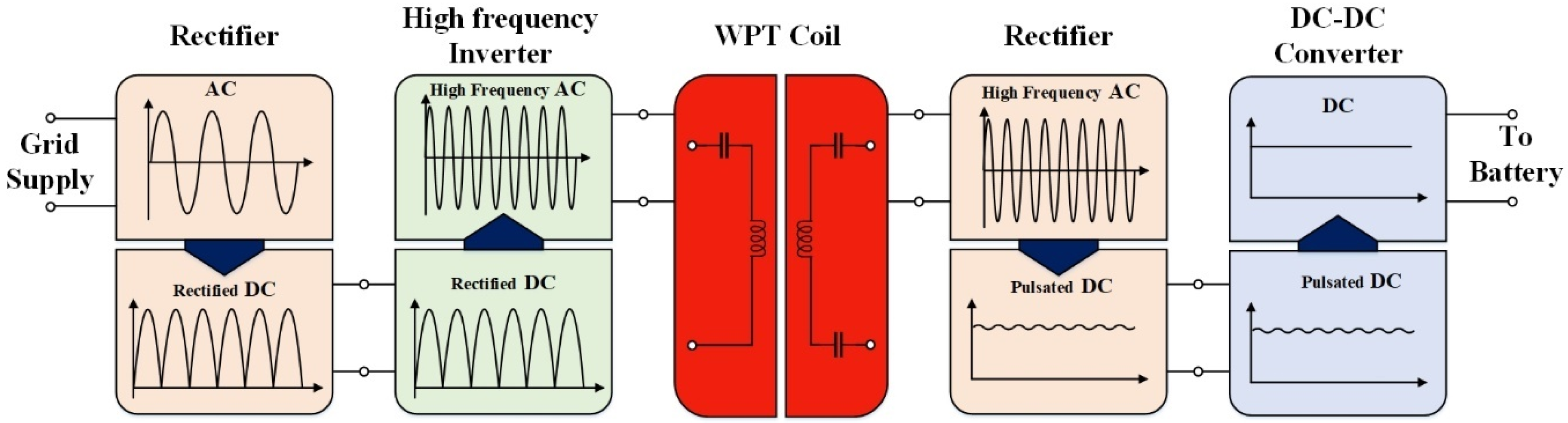
2. Switching Characteristics of a WPT HF Inverter

The SS, SP, PS, and PP topologies in the WPT system have varying complexity, resonance behavior, and efficiency. The DS-LCC and DS-LCL configurations offer design flexibility but may increase complexity. The LCC-LCL topology combines LCC and LCL advantages, offering robust resonance characteristics, efficient power transfer, and reduced load sensitivity. It is preferred for its balanced performance and flexibility in WPT applications. The LCC-LCL WPT system is used for DT analysis. The circuit of the LCC-LCL WPT structure is given in Figure 2.
The LCC-LCL topology consists of few resonant devices; L1t, Ct1, Ct2 and Lr, Cr are the primary and secondary compensation parameters. Vidc and Iidc represent the DC input voltage and current on the primary side, while Vldc and Iidc denote the DC output voltage and current on the secondary side across the load RL. L1 and L2 are the self-inductances of the transmitting and receiving coils, respectively, with M being the mutual inductance between them. S1–S4 are the MOSFETs, D1–D4 are the body diodes, and D5 to D8 are the receiver side bridge rectifier diodes. The primary and secondary HF inverter voltages and currents are denoted as U1xy, U2pq, i1, and i2 respectively. The LCC-LCL compensation inductances and capacitors, and the dc load, are assumed to be purely resistive. The conventional WPT system illustration transforms into a Zr equivalent circuit, featuring MOSFET switches (S1–S4) of the full-bridge inverter, connected across phase legs, as shown in Figure 3.
There are several common control approaches used on full-bridge inverters, such as PWM and PDM, which are essential control methods in the WPT system for the efficient delivery of power and the management of inverters. PWM regulates the amplitude of the output voltage by adjusting the breadth of pulses within a fixed-frequency waveform. This method is extensively used due to its simplicity and efficacy in regulating power levels and maintaining resonance in WPT applications. PDM, in contrast, modulates the density or distribution of pulses within a fixed time period, providing a higher degree of resolution and the potential for lower switching losses than PWM. PDM is advantageous in situations that necessitate precise control over power delivery while simultaneously minimizing electromagnetic interference. PWM and PDM techniques are both instrumental in the optimization of efficiency and performance in the WPT system, thereby addressing a wide range of operational challenges and application requirements.

2.1. Pulse Density Modulation

The gate pulse waveforms for PWM and PDM are illustrated in Figure 4a without dead time and Figure 4b with dead time inserted. The output voltage is regulated by PWM, which maintains a consistent frequency by adjusting the pulse breadth. In order to attain the intended voltage levels, this modulation technique modifies the duty cycle. Conversely, PDM regulates its RMS output voltage by selectively omitting specific pulses in accordance with a predetermined control sequence, rather than by modifying pulse breadth. By applying the magnitude density (D) balance principle, it is possible to determine the RMS value of the fundamental component of U1xy.
U 1 x y = 2 2 π D V i d c ,
It is crucial to guarantee that the pulses in PDM are uniformly distributed in order to reduce power fluctuations within the system. This requirement implies that PDM cannot be accomplished by solely eliminating pulses from the original sequence. Figure 5 illustrates a PDM logic circuit that consists of a hardware-based dead-time integrated logic-based pulse generator. The trigger pulse signal with a frequency of fsw and a specified pulse density of D is one of the input signals to this system. The pulse generator generates two reference pulses, Uxref and Uyref, by operating at a frequency that is twice the switching frequency fsw. Following their passage through the dead-time generator, these pulses are transformed into two pairs of complementary driving signals, each of which includes a dead-time constant (td).
The average power transfer of the WPT system with PDM can be regulated by adjusting D and td, according to
P = 2 2 π ( D × t d T )   V i d c I i d c   cos φ ,
In the WPT system, using PDM, current and power fluctuations occur due to skipped pulses. However, applying PWM reduces sending voltage perturbations by half. This is achieved by doubling the accumulator’s trigger frequency, accounting for both the rising and falling edges of the input pulse. Understanding the impact of dead time is crucial for analyzing the characteristics of switching with and without it. The effects of dead time on output voltage and currents will be discussed in the next section.

2.2. Characteristics of Switching with Zero Dead-Time

The operation of the switching characteristics using the equivalent circuit shown in Figure 3, with an inverter with zero dead time, is given in Figure 6. While this is not feasible in practice, it provides a foundation for further analysis. In Figure 6a, the waveform Gi represents the gate pulses of the MOSFET switches S1 to S4. Uxo and Uyo represent the voltages at the poles of the inverter phase legs, while Uxy represents the square-wave voltage across the inverter phase legs. The red dashed sine wave Uxy is the primary element of the inverter’s output voltage. The blue sine wave ixy represents the sinusoidal current flowing through the load impedance, with the phase angle (ϕ) between the basic voltage component and the sinusoidal current.
Figure 6b represents the current flow path (red dashed line) according to the switch transition states of operation of the high-frequency inverter, as explained in Table 1 with the current flow direction and the output voltage.

2.3. Characteristics of Switching with Dead Time

The DT is the period among the swapping events of complementary MOSFETs in an inverter leg. During this interval, both MOSFETs are OFF, and the current flows through their body diodes. If the current reverses during the dead time, the pole voltages also reverse, causing a notch in the inverter output that adversely affects the system’s output voltage. It has been determined that notches in the inverter output can be avoided by satisfying the notch equation defined by Equation (3).
| θ v ϕ | δ t d 2 ,
The angle θv represents the difference between the square wave voltage and its fundamental component. It is calculated as θv = α/2 using the standard phase-shift control technique, where α is the phase-shift angle between the inverter phase legs. The symbol δtd represents the angle of dead time, as defined by
δ t d = 2 π × f s w × t d ,
td is the dead time in seconds and fsw is the switching frequency in Hz. Please note that the phase-shift angle (α) and phase angle (ϕ) are assumed to be ≥0, and the phase-shift control between the inverter legs is defined to result in a full duty cycle at the output at 0° phase shift and zero duty cycle at 180° phase shift. The WPT system aims to maintain the desired output voltage/current levels; hence, ϕ and α operating conditions were chosen to study the notch behavior. The corresponding switching characteristics with the dead time and the generation of a signal will be explained in switch transition states, as shown in Figure 7.
Figure 7a represents the gate pulses, leg voltages, output voltages, and current wave forms. In Figure 7a, the switch transition states of operation of the high-frequency inverter are explained as the current flow path (red dashed line) direction and the output voltage according to Table 2.
Dead time in two-phase inverters with MOSFET’s is crucial for efficient operation and generating distortion in output waveform. However, it can introduce challenges in high efficiency and power transfer, as deviations from rectangular pulses affect effective energy transfer. The next section addresses the impact of dead time in fundamental parameters and modeling of the resonant network.

3. Effects of Dead Time on the Fundamental Components

From the previous section, WPT system’s switching states are caused by the current flow direction changes during dead time. These alterations cause MOSFET body diodes to conduct, causing unwanted inverter output switching. When the current polarity changes during dead time, the pole voltages change, disrupting the inverter output’s volt-second integral. This affects the square-wave voltage’s basic element and harmonic dispersion.

3.1. Theoretical Derivation of the HF Inverter Output Voltage in WPT

This section describes the mathematical equations for the inverter waveform with the notch and evaluates its impact on the fundamental component and harmonics. A traditional HF inverter output voltage and current waveform with notch is given in Figure 8.
The output voltage of the inverter is expressed as a Fourier series form:
U x y = x 0 + n = 1 x n cos n ω t + y n sin n ω t
The Fourier coefficient, x0 = 0, xn = 0 (for all even values of n,), and yn are estimated as follows due to the waveform’s half-wave and odd symmetry:
y n = 1 π 0 2 π f ( x ) sin n ω t   d ω t ,
Here, f(x) is the periodic function (wave form Uxy) represented in Figure 8. By solving (5), the following equation is given:
y n = V i d c n π [ 2 cos n δ 1 + cos n δ 2 + cos n δ 3 cos n δ 4 cos n δ 5 + 2 cos n δ 6 cos n δ 7 cos n δ 8 + cos n δ 9 + cos n δ 10 ] ,
The angle δi is determined by the operating circumstances of phase angle (ϕ), phase shift (α), and dead-time angle (δtd). In Figure 8, the notch appears twice in the square waveform half-cycle.
U x y n = y n 2 = V i d c 2 n π [ 2 cos n δ 1 + cos n δ 2 + cos n δ 3 cos n δ 4 cos n δ 5 + 2 cos n δ 6 cos n δ 7 cos n δ 8 + cos n δ 9 + cos n δ 10 ] ,
U x y n = V i d c 2 n π c δ i
The above mathematical expressions are used to find the output parameters for the load-connected HF inverter leg equivalent circuit shown in Figure 3. By using Equations (8) and (9), we can analyze how dead time affects the fundamental output voltage and its harmonics in a HF inverter used for WPT. This analysis considers both PDM and PWM controls. Figure 9a,b show that the theoretical predictions match the actual results quite well. Specifically, Figure 9b demonstrates how varying dead time impacts the fundamental component of the HF inverter voltage in an LCC-LCL resonant circuit. The results indicate that the fundamental component values change depending on the different density and dead time used in both PDM and PWM control methods. The loss of inverter at 0.8 density PDM is ~6.0% for a DT of 1 μs, as shown in Figure 9b. Inverter duty cycle loss is approximately 8% at 85 kHz operating frequency with the same DT value. As the working frequency increases, the fundamental component of the inverter decreases, causing the DT effect. According to the harmonic order, for the given operating condition, the inverter output notch raises the voltage, which decreases the higher-order harmonics and lowers the lower-order harmonics. Moreover, it is evident from comparing Figure 9a,b that changing the density of PDM of the inverter can regulate its harmonic content. The resonant network suppresses higher order harmonics by allowing just the inverter’s fundamental component to couple with the secondary.
However, inverter square-wave harmonic content may increase MOSFET switch switching losses and thermal pressures. Should the voltage/current strains brought on by the notch surpass the acceptable bounds, the MOSFET switch could sustain irreversible damage. In the forthcoming section, we will delve into the essential considerations of selecting the resonance compensation network and accurately calculating its parameters, taking into account the significant influence of dead time. Furthermore, the overall system efficiency will be impacted by the rise in the switching losses. The loss of essential component affects the features of the WPT system as well as this, and will be covered in the next section.

3.2. Modeling of Resonance Compensation Network for WPT

From Figure 2, selecting the compensation topology and deriving the value of the components for the LCC-LCL WPT system can achieve high efficiency and reliable power transfer, even when considering the effects of dead time in PDM. The LCC-LCL topology is a hybrid resonant converter that combines series and parallel resonance strengths. It consists of an LCC network and an LCL network, creating a robust resonant tank for efficient power transfer and improved voltage regulation. The LCC stage shapes the resonant frequency and control voltage, reducing switching losses and electromagnetic interference. The LCL stage refines power delivery, ensuring minimal harmonic distortion and improved load regulation. Figure 10 reflects the equivalent circuit of a magnetic resonance WPT EV charger with LCC-LCL compensation networks.
The primary inductor (L1), resonant inductors (Lt), and capacitors (Ct1 and Ct2) form the resonant tank circuit on the transmitter side, generating the high-frequency AC signal. The mutual inductance (LM) between L1 and the equivalent secondary inductor (L2e) enables energy transfer. On the receiver side, the capacitor (Cre), inductor (Lre), and load resistance (RLe) form the resonant circuit that captures and converts the transmitted power. The input voltage (U1) drives the circuit, creating an input current (Ixy) that induces a magnetic field in Lt, coupling to L2e. The load current (IL) and voltage (VLdc) are delivered to RLe, representing the transferred power. Proper component selection and tuning achieve high efficiency and reliable power transfer, accounting for the dead-time effects in PDM.
The mutual inductance represents the coupling between the primary and secondary coils in a WPT system. The value of mutual inductance depends on the geometry of the coils, their distance, and their orientation. The mutual inductance (LM) between two coils can be expressed as
L M = k L 1 L 2 ,
where k is the coupling coefficient (ranges from 0 to 1, with 1 being perfect coupling). The coupling coefficient (k) is defined as
k = L M L 1 L 2 ,
In a static wireless EV charging system, parallel compensation involves capacitors across the stator coil terminals. These compensation capacitors are carefully placed in series and parallel on the transmitter and receiver. Source compensation aims to remove the current–voltage phase mismatches, output current ripples, and reduce the reactive power drawn from the source. In the WPT system, the primary and secondary resonant frequencies are identical. The resonant frequency for the primary side LCC network (Lt, Ct1, and Ct2) can be found using the series and parallel combinations of the inductors and capacitors. For a series–parallel combination,
1 r 1 2 = L t ( C t 1 + C t 2 ) ,
r 1 = 1 L t ( C t 1 + C t 2 )
The primary side resonant frequency (fr1) is
f r 1 = r 1 2 π = 1 2 π L t C t 1 + C t 2 ,
The resonant frequency for the secondary side LCL network (L2e, Cre, Lre) can be found using the series and parallel combinations of the inductors and capacitors. For a series–parallel combination,
1 r 2 2 = L 2 e ( C r e + L r e L r e + L 2 e )
r 2 = 1 L 2 e ( C r e + L r e L r e + L 2 e )
The secondary side resonant frequency (fr2) is
f r 2 = r 2 2 π = 1 2 π L 2 e ( C r e + L r e L r e + L 2 e )
In order to eliminate the reactance in Equation (15), the secondary tank must resonate at a specific angular frequency (ω0).
0 = r 1 = r 2 = 1 L t ( C t 1 + C t 2 ) = 1 L 2 e ( C r e + L r e L r e + L 2 e )
Dead-time analysis considers the mutually connected state with the first harmonic approximation (FHA). Calculate the RMS primary-side AC voltage from Expression (9) U1xy, as
U 1 x y = V i d c 2 n π C δ i ,
where Cδi is determined in Section 3.1 and depends on the operating conditions of α and ϕ. The AC voltage and current at the input of the secondary rectifier are described as follows:
U 2 p q = 2 2 π V l d c ,
i 2 = π 2 2 I l d c
U2pq and i2 are the AC voltage at the input to secondary rectifier and the current streaming through the receiver coil. The equivalent load resistance at the input of the diode rectifier is written as
R L e = 8 R L L t   π 2 L r ,
L t 1 = L t 1 ( 1 k )
L m = k   L t 1
L 2 e = L t
C r e = C t 1 L r   L t
L r e = L r 1 L t 1   L r
From the above Expression (18), the design value for the inductor Lt1 capacitors Ct1 and Ct2 in the primary resonant network is
L t 1 = 2 2 π × V l d c 0 2 I R l o a d × L r L t ,
C t 1 = 1 0 2 L t 1 + 1 0 2 ( ( 1 k ) L t )
C t 2 = 1 0 2 ( L t L t 1 )
The transmitter side impedance of the WPT is expressed as
Z t = j ω L t + 1 j ω C r 2 + j ω L 1 | | 1 j ω C t 1 ,
Z t = j ω L t + 1 j ω C r 2 + L 1 j ω C t 1
The receiver side impedance of the WPT is derived as
Z s e c = R L e + j ω L 2 e + 1 j ω C r e + j ω L r e
The receiver side impedance reflected on transmitter side impedance is defined as
Z r e f l e c t = Z s e c k 2
The total input impedance, when combined with the primary side impedance and the reflected impedance:
Z i n = Z t + Z r e f l e c t
The input impedance Zin seen by the source U1:
Z i n = j ω L t + 1 j ω C t 2 + L 1 j ω C t 1 + Z s e c k 2
The load impedance:
Z l o a d = Z s e c
Z l o a d = R L e + j ω L 2 e + 1 j ω C r e + j ω L r e
A mesh-based analysis results in
U 1 x y = j ω L t + 1 j ω C t 2 + L 1 j ω C t 1 + Z s e c k 2 I x y
U 2 p q = R L e + j ω L 2 e + 1 j ω C r e + j ω L r e I 2
The overall WPT efficiency:
η = P L P i n = I L 2 R L e U 1   I x y cos φ
The transconductance gain:
G m = I l d c U 1 x y = j ω L M Z i n   Z s e c
The voltage gain:
G v = V L d c U 1 x y = j ω L M R L e Z i n   Z s e c
The current gain:
G i = I L d c I x y = j ω L M   Z s e c
IL is the load current and Vldc is the load voltage. Using Equations (21)–(28), the parameters for the LCC-LCL resonant compensation network are calculated and shown in Table 3. These parameters are used in the subsequent simulation and experiment, as illustrated in Figure 3. A detailed analysis of these findings is provided in Section 4.

4. Dead-Time Effects in WPT System via Simulation and Experimental

The behavior of dead time involved in the PDM-based controlled LCC-LCL WPT system is designed and simulated in MATLAB/Simulink 2023a software as per the schematic circuit diagram given in Figure 2. For the simulation design, the compensation network values were referred from Table 3 and WPT design values were referred from Table 4. The theoretical model is verified through simulations, and the output parameters are validated through the WPT prototype experimental setup shown in Figure 11 using the parameters values given in Table 4. The WPT system is made up of ONSEMI NTHL080N120SC1 SiC 1200 V/35 A MOSFET, and full-bridge arrangement modules are driven by Texas Instruments (Dallas, TX, USA) UCC27531A gate-drivers (Fall Time 7 ns, Rise Time 15 ns, Turn-Off and ON delay time 17 ns). Selecting an appropriate dead time as a percentage of the switching period (T) helps standardize its selection across different frequencies. For low-frequency applications (20 kHz–100 kHz), the dead time typically ranges from 1% to 15% of T. In medium-frequency applications (100 kHz–500 kHz), the dead time usually falls between 1% and 25% of T. For high-frequency applications (500 kHz–1 MHz), the dead time generally ranges from 5% to 20% of T. To ensure safe operation of the MOSFET inverter at a switching frequency of 85 kHz, the chosen dead time values of 0.5 μs, 1.0 μs, 1.5 μs, and 2.0 μs should be selected based on these percentages. In order to supply the full-bridge inverter, gate pulses from a Spartan-6 FPGA control board are utilized. The analysis shows how the dead time affects system sensitivity under a constant operating frequency of 85 KHz, with a resistive load of 22 Ω and different PDM density level of (D = 0.2, 0.5, 0.8), assuming the unity power factor.
The LCC-LCL topology is the where the main capacitor’s correct value is not affected by the load impedance. The fact that Co is dependent on RL makes it hard to use in real life. There is a link between the secondary capacitor and the monoresonant compensation network that changes how the system works. The primary-side and secondary-side LCC-LCL compensation parameters were assembled with Celem Power Capacitors CSP 120/200 conduction-cooled capacitors according to the intended values in Table 3. The secondary side rectifier uses 600 V/100 A APT2X101DQ60 J (Mouser Electronics, Mansfield, TX, USA) ultrafast phase-leg rectifiers.

5. Analysis of Simulation and Experimental Results

The design optimization and efficiency predictions are facilitated by the powerful instrument of MATLAB simulation, which is capable of modeling and evaluating the performance of WPT EV chargers. The subsequent step in the hardware results analysis is to test the tangible WPT charger to ensure that it complies with the design specifications and functions efficiently in real-world charging scenarios.

5.1. Simulation Results and Discussions

The MATLAB simulation results are discussed in this section as graphical representation. Figure 12 illustrates the effect of various dead-time values (500 ms, 1000 ms, 1500 ms, and 2000 ms) of the switching gate pulses for the WPT HF inverter and the corresponding output voltage and current waveforms. As the dead time increases, the inverter’s output characteristics decreases, demonstrating variations in the voltage and current profiles. The focus is on the dead-time impact with constant operating frequency, mutual inductance, and load. When comparing the theoretical analysis from Figure 9 and the simulated results, the fundamental output voltages of the HF inverter for WPT shows 3% to 5% minimal variation for the different harmonics order.
The simulation results of the input gate pulses with different dead time values, output voltages, and current wave forms of HF inverter WPT with PDM (D = 0.2) control are given in Figure 13.
The HF inverter WPT simulation results of input gate pulses with different dead time values, output voltages, and current wave forms for PDM (D = 0.5) control are given in Figure 14.
Figure 13, Figure 14 and Figure 15 shows how the dead-time intervals affect the WPT system HF inverter PDM switching gate pulses at different densities (D) 0.2, 0.5, and 0.8; output voltage; and current waveforms. The top-row sub-diagrams display HF inverter switching gate pulses with 500 ms, 1000 ms, 1500 ms, and 2000 ms dead-time settings. Shoot-through is prevented by widening the spacing between complimentary MOSFET switching occurrences as dead time grows. The central diagram shows the HF inverter output voltage (magenta) and current (orange) over time, with arrows showing precise moments corresponding to detailed waveforms in the bottom row. The bottom-row insight show a single cycle of HF inverter output voltage and current waveforms with notch when dead time is inserted. The waveforms show the trade-off between shoot-through and waveform integrity and efficiency. The probability of waveform aberrations and shoot-through is shown without dead-time. Intermediate dead times (0.5 µs to 1.0 µs) minimize risk and maintain waveform quality. However, excessive dead-time (1.5 µs to 2.0 µs) might cause notching and inefficiency. From the simulation results, the inverter voltage, current, input DC power, output AC power, transmitter and receiver coil power, and output dc load power are observed, and the current ripples are calculated for different dead-time values and PDM density levels. This analysis shows how dead-time intervals affect HF inverter switching and output in a WPT system. Using Equations (39)–(41), the parameters are derived and shown graphically below for easy understanding.
Figure 16 illustrates the performance comparison of Pulse Density Modulation at a density of 0.8 and 0.5, along with Pulse Width Modulation at duty cycle 50%, across different metrics, while the dead time increases from 0% to 20% in the 85 kHz WPT system. Comparing Figure 16a–d, we observe that the reduction in the inverter duty cycle due to dead time impacts the DC voltage gain and transconductance gain of the system.
As dead time increases, all input DC voltage gains diminish, as shown Figure 16a. PDM with D = 0.8 has the most gain, while PWM has the lowest. Figure 16b indicates that PDM D = 0.8 initially has a greater input DC current gain, but it drops drastically after a 15% dead period. The PWM has a little current amplification advantage at most dead moments, but the PDM with a density of 0.5 has similar patterns.
All approaches show a drop in input AC voltage gain as dead time increases, as shown in Figure 16c. PDM D = 0.8 consistently yields the highest gain, while PDM D = 0.5 and PWM perform similarly, with PWM slightly outperforming at longer dead times. Figure 16d shows that all techniques enhance transconductance as dead time increases.
PDM D = 0.8 has the highest values, especially for longer dead times, while PWM has the lowest. As dead time rises, the input DC power decreases, as shown in Figure 16e. The PDM D = 0.8 arrangement offers the highest power at shorter dead times but rapidly diminishes after 10%. However, PWM uses the least electricity. As dead time rises, all DC power output loads decrease, as shown Figure 16f. PDM with a duty cycle of 0.8 reduces power by 15% of the dead time, while PWM has the lowest power.
Dead time is negatively correlated with transmitter AC power, as shown in Figure 16g. It shows that PDM D = 0.8 produces the maximum power, especially at lower dead times, while PWM produces the least. As dead time increases, the receiver AC power drops, as shown in Figure 16h. PDM D = 0.8 has the highest power for most dead periods, while PWM has the lowest. PDM with D = 0.8 often preserves better gains and power levels than PDM with D = 0.5 and Pulse Width Modulation. PWM performs the worst in several metrics as dead time increases.
Higher dead-time hurts all performance indicators; however, the degree depends on modulation methods. From the above graphical analysis, the impact of dead time in the WPT EV charger performance parameters are calculated and tabulated for PMW and PDM control, as shown in Table 5.
Table 5 presents a comparison of the performance of the Pulse Width Modulation and Pulse Density Modulation control approaches for the WPT HF inverter. The comparison is performed for PDM densities of 0.5 and 0.8 both with and without dead time. It demonstrates that PDM typically leads to reduced power dissipation and increased transfer efficiency in comparison to the PWM control technique. Furthermore, PDM demonstrates superior efficiency compared to PWM as dead time increases, emphasizing its ability to minimize power loss and enhance performance.

5.2. Expermental Results and Discussions

Figure 17a illustrates the voltage and current waveforms of a HF inverter used in WPT, showing smooth voltage transitions and a current waveform with a noticeable ripple. Figure 17b displays the PWM control signals, highlighting the gate pulses and the resulting inverter current waveform.
Figure 18 illustrates notch occurrence when the voltage is predominantly increasing in width, when the dead time increases, and when a current waveform has decreasing ripples.
Figure 19 consists of (a), (c), (e), and represents the inverter output voltage and current for different PDM densities of 0.2, 0.5, and 0.8. As shown in Figure 19b,d,f, each result illustrates the high-frequency inverter switching gate pulses with the respective densities (D = 0.2, 0.5, 0.8) without dead time inserted.
From Figure 20, the presence of a PDM of 0.2 results in a noticeable effect of increasing dead time and affects the higher frequency of voltage. The notch width also increases, which causes a substantial amount of harmonic distortion in the output signal.
From Figure 21, the presence of a PDM of 0.5 results in a noticeable effect of increasing dead time and affects the higher frequency of voltage. The notch width also increases, which cause a substantial amount of harmonic distortion in the output signal.
From Figure 22, the presence of a PDM of 0.8 results in a noticeable effect of increasing dead time and affects the higher frequency of voltage. The notch width also increases, which cause a substantial amount of harmonic distortion in the output signal.
The recurring notches and its width increases are observed in Figure 20, Figure 21 and Figure 22. When dead time increases, that leads to temporary conduction through the MOSFET body diodes. These notches, along with the accompanying current waveform fluctuations, illustrate the influence of dead time on the current flow, causing directional changes and transient disruptions. Such disturbances adversely affect the overall performance and efficiency of the WPT system. This underscores the critical need for precise dead-time management to minimize these disruptions and ensure stable, efficient power transfer. Comparing PWM-controlled inverter results with PDM control results, less current ripples are observed. Figure 23 illustrates current ripple variations for PWM and PDM at different dead times from the experimental and simulation output.
It shows that the current ripple decreases as dead time increases for a 50% duty cycle in PWM control. Similarly, it decreases with increasing dead time across all pulse densities, with the most significant reduction observed at lower pulse densities like 20% in PDM control. As dead time increases, the current at the rectifier input reduces from ~18 to ~10 due to parasitic components, as observed in experimental waveforms. The MATLAB analysis aligns well with experimental findings. Additionally, the study compares inverter output voltage harmonics with and without notches at full duty cycle. Notching reduces lower-order harmonics while elevating higher-order harmonics under the specified operating conditions. Harmonic levels are adjustable by varying the inverter phase-angle and duty cycle. However, increased harmonics may escalate switching losses and stress on MOSFET switches, potentially causing permanent damage and impacting overall system efficiency. Table 6 compares the performance of PWM and PDM control techniques in HF inverters, highlighting the impact of dead time of 1µs on the voltage gain, current ripple ratio, and efficiency. Notably, PDM with dead time shows a significant improvement in the efficiency and current ripple ratio compared to other configurations. Comparing the results of PDM and PWM implementations reveals that PDM offers better performance in terms of efficiency and stability to the HF WPT inverter for EV charging applications.
Table 6 validates that PDM techniques outperform PWM in HF inverter applications, achieving higher voltage gain and efficiency with lower current ripple ratios compared with other papers in the literature. Additionally, implementing dead time improves overall performance, with PDM (0.8 µs) showing the best results.

6. Conclusions

This work addresses the PDM control technique used in wireless transmission to reduce the impact of and maximize power over the PWM control. The impact of dead time in HF inverters shows the variations in the current direction during VPR occurrence, reducing the inverter output voltage by up to 5%. Notches affected the HF inverter, the fundamental component of the voltage, and impacted the harmonic spectrum but reduced the current ripples by 10%. The prediction of notches in the HF inverter voltage is performed using the notch equation, allowing harmonic control through various combinations of input dead time and pulse density. Dead-time effects can be lessened with the help of compensation topologies such as the LCC-LCL, which also generally enhances system performance, efficiency, and power quality by reducing the current ripples and reducing the power dissipation from 20% to 10% for increasing dead-time values. The study finds that dead time lowers the power delivered to the load, increasing the transconductance gains. A prototype 3.7 kW WPT system with a maximum efficiency of 92% was used to compare the experimental results and validation results with the theoretical expectations. Further, future work will focus on optimizing PDM techniques for investigating an adaptive control strategy to dynamically adjust for varying load conditions and environmental factors with improved dead-time management in WPT EV systems.

Author Contributions

Methodology, F.J., P.R.G.K. and N.R.; Software, J.P.; Validation, V.K.; Formal analysis, V.K.; Investigation, F.J., P.R.G.K., L.V. and J.P.; Resources, N.R. and L.V.; Data curation, V.K.; Writing—original draft, F.J.; Writing—review & editing, P.R.G.K., N.R. and J.P.; Funding acquisition, L.V. All authors have read and agreed to the published version of the manuscript.

Funding

This work was supported by the Council of Scientific & Industrial Research (CSIR), India, under EMR II research scheme 22/0901/23/EMR-II. This research was also supported by the SGS grant from VSB—Technical University of Ostrava under grant number SP2024/018.

Institutional Review Board Statement

Not applicable.

Informed Consent Statement

Not applicable.

Data Availability Statement

All the data used for this study are available within the manuscript.

Conflicts of Interest

The authors declare no conflicts of interest.

References

  1. Kwilinski, A.; Lyulyov, O.; Pimonenko, T. Environmental Sustainability within Attaining Sustainable Development Goals: The Role of Digitalization and the Transport Sector. Sustainability 2023, 15, 11282. [Google Scholar] [CrossRef]
  2. Shanmugam, Y.; Narayanamoorthi, R.; Vishnuram, P.; Bajaj, M.; Aboras, K.M.; Thakur, P. A Systematic Review of Dynamic Wireless Charging System for Electric Transportation. IEEE Access 2022, 10, 133617–133642. [Google Scholar] [CrossRef]
  3. Zhang, W.; Fang, X.; Sun, C. The Alternative Path for Fossil Oil: Electric Vehicles or Hydrogen Fuel Cell Vehicles? J. Environ. Manag. 2023, 341, 118019. [Google Scholar] [CrossRef] [PubMed]
  4. Abdel-Basset, M.; Gamal, A.; Hezam, I.M.; Sallam, K.M. Sustainability assessment of optimal location of electric vehicle charge stations: A conceptual framework for green energy into smart cities. Environ. Dev. Sustain. 2024, 26, 11475–11513. [Google Scholar] [CrossRef]
  5. Su, F.; He, X.; Dai, M.; Yang, J.; Hamanaka, A.; Yu, Y.; Li, J. Estimation of the cavity volume in the gasification zone for underground coal gasification under different oxygen flow conditions. Energy 2023, 285, 129309. [Google Scholar] [CrossRef]
  6. Dimitriadou, K.; Rigogiannis, N.; Fountoukidis, S.; Kotarela, F.; Kyritsis, A.; Papanikolaou, N. Current Trends in Electric Vehicle Charging Infrastructure; Opportunities and Challenges in Wireless Charging Integration. Energies 2023, 16, 2057. [Google Scholar] [CrossRef]
  7. Sagar, A.; Kashyap, A.; Nasab, M.A.; Padmanaban, S.; Bertoluzzo, M.; Kumar, A.; Blaabjerg, F. A Comprehensive Review of the Recent Development of Wireless Power Transfer Technologies for Electric Vehicle Charging Systems. IEEE Access 2023, 11, 83703–83751. [Google Scholar] [CrossRef]
  8. Liu, W.; Chau, K.; Tian, X.; Wang, H.; Hua, Z. Smart wireless power transfer—opportunities and challenges. Renew. Sustain. Energy Rev. 2023, 180, 113298. [Google Scholar] [CrossRef]
  9. Sari, V. Design and Implementation of a Wireless Power Transfer System for Electric Vehicles. World Electr. Veh. J. 2024, 15, 110. [Google Scholar] [CrossRef]
  10. Zhang, J.; Liu, Y.; Zang, J.; Liu, Z.; Zhou, J.; Wang, J.; Shi, G. An Embedded DC Power Flow Controller Based on Full-Bridge Modular Multilevel Converter. IEEE Trans. Ind. Electron. 2024, 71, 2556–2566. [Google Scholar] [CrossRef]
  11. Vishnuram, P.; Panchanathan, S.; Rajamanickam, N.; Krishnasamy, V.; Bajaj, M.; Piecha, M.; Blazek, V.; Prokop, L. Review of Wireless Charging System: Magnetic Materials, Coil Configurations, Challenges, and Future Perspectives. Energies 2023, 16, 4020. [Google Scholar] [CrossRef]
  12. Wang, Y.; Sun, Z.; Guan, Y.; Xu, D. Overview of Megahertz Wireless Power Transfer. Proc. IEEE 2023, 111, 528–554. [Google Scholar] [CrossRef]
  13. Rayan, B.A.; Subramaniam, U.; Balamurugan, S. Wireless Power Transfer in Electric Vehicles: A Review on Compensation Topologies, Coil Structures, and Safety Aspects. Energies 2023, 16, 3084. [Google Scholar] [CrossRef]
  14. Yin, Y.; Xiao, Y.; Wang, C.; Yang, Q.; Jia, Y.; Liao, Z. A Design Methodology for EV-WPT Systems to Resonate at Arbitrary Given Bands. Energies 2022, 15, 213. [Google Scholar] [CrossRef]
  15. Zhang, J.; Feng, X.; Zhou, J.; Zang, J.; Wang, J.; Shi, G.; Li, Y. Series-Shunt Multiport Soft Normally Open Points. IEEE Trans. Ind. Electron. 2023, 70, 10811–10821. [Google Scholar] [CrossRef]
  16. Ahire, D.B.; Gond, V.J.; Chopade, J.J. Compensation topologies for wireless power transmission system in medical implant applications: A review. Biosens. Bioelectron. 2022, 11, 100180. [Google Scholar] [CrossRef]
  17. Ramakrishnan, V.; Dominic Savio, A.; Balaji, C.; Rajamanickam, N.; Kotb, H.; Elrashidi, A.; Nureldeen, W. A Comprehensive Review on Efficiency Enhancement of Wireless Charging System for the Electric Vehicles Applications. IEEE Access 2024, 12, 46967–46994. [Google Scholar] [CrossRef]
  18. Feng, J.; Wang, Y.; Liu, Z. Joint impact of service efficiency and salvage value on the manufacturer’s shared vehicle-type strategies. RAIRO-Oper. Res. 2024, 58, 2261–2287. [Google Scholar] [CrossRef]
  19. Ju, Y.; Liu, W.; Zhang, Z.; Zhang, R. Distributed Three-Phase Power Flow for AC/DC Hybrid Networked Microgrids Considering Converter Limiting Constraints. IEEE Trans. Smart Grid 2022, 13, 1691–1708. [Google Scholar] [CrossRef]
  20. Poornima, P.U.; Elanthirayan, R.; Pongiannan, R.K.; Pravin, A.R.; Franklin, J.; Brindha, R. A Single Phase Cascaded H Bridge PV Inverter’s Harmonic Compensation Strategy in an Unbalanced Condition. In Proceedings of the 2023 International Conference on System, Computation, Automation and Networking, Puducherry, India, 17–18 November 2023. [Google Scholar]
  21. Aretxabaleta, I.; De Alegria, I.M.; Andreu, J.; Kortabarria, I.; Robles, E. High-Voltage Stations for Electric Vehicle Fast-Charging: Trends, Standards, Charging Modes and Comparison of Unity Power-Factor Rectifiers. IEEE Access 2021, 9, 102177–102194. [Google Scholar] [CrossRef]
  22. Li, S.; Yu, X.; Yuan, Y.; Lu, S.; Li, T. A Novel High-Voltage Power Supply with MHz WPT Techniques: Achieving High-Efficiency, High-Isolation, and High-Power-Density. IEEE Trans. Power Electron. 2023, 38, 14794–14805. [Google Scholar] [CrossRef]
  23. Liu, C.; Guan, Y.; Wang, Y.; Xu, D. Optimal Impedance Design for Dual-Branch High-Frequency Inverter Based on Active Regulation and Passive Projection. IEEE Trans. Power Electron. 2023, 38, 11183–11192. [Google Scholar] [CrossRef]
  24. Viqar, S.; Ahmad, A.; Kirmani, S.; Rafat, Y.; Hussan, M.R.; Alam, M.S. Modelling, Simulation and Hardware Analysis of Misalignment and Compensation Topologies of Wireless Power Transfer for Electric Vehicle Charging Application. Sustain. Energy Grids Netw. 2024, 38, 101285. [Google Scholar] [CrossRef]
  25. Ding, Z.; Huang, Z.; Pang, M.; Han, B. Design of Bi-Planar Coil for Acquiring Near-Zero Magnetic Environment. IEEE Trans. Instrum. Meas. 2022, 71, 6001310. [Google Scholar] [CrossRef]
  26. Marques, E.G.; Costa, V.S.; Mendes, A.M.S.; Perdigao, M.S. Inductive Power Transfer in Electric Vehicles: Past and Future Trends. IEEE Veh. Technol. Mag. 2023, 18, 111–122. [Google Scholar] [CrossRef]
  27. Zhao, H.; Liu, K.; Li, S.; Yang, F.; Cheng, S.; Eldeeb, H.H.; Kang, J.; Xu, G. Shielding Optimization of IPT System Based on Genetic Algorithm for Efficiency Promotion in EV Wireless Charging Applications. IEEE Trans. Ind. Appl. 2022, 58, 1190–1200. [Google Scholar] [CrossRef]
  28. Pongiannan, R.K.; Yadaiah, N. FPGA Based Space Vector PWM Control IC for Three Phase Induction Motor Drive. In Proceedings of the 2006 IEEE International Conference on Industrial Technology, Mumbai, India, 15–17 December 2006. [Google Scholar]
  29. Zhou, J.; Guidi, G.; Chen, S.; Tang, Y.; Suul, J.A. Conditional Pulse Density Modulation for Inductive Power Transfer Systems. IEEE Trans. Power Electron. 2024, 39, 88–93. [Google Scholar] [CrossRef]
  30. Cetin, S.; Yenil, V. High Efficiency Constant Voltage Control of LC/S Compensated Wireless Power Transfer Converter Based on Pulse Density Modulation Control. Int. J. Electron. 2023, 110, 54–72. [Google Scholar] [CrossRef]
  31. Pongiannan, R.K.; Sathiyanathan, M.; Vinothkumar, U.; Junaid, K.M.; Prakash, A.; Yadaiah, N. FPGA—Realization of Digital PWM Controller Using Q-Format-Based Signal Processing. JVC J. Vib. Control. 2015, 21, 938–948. [Google Scholar] [CrossRef]
  32. Franklin, J.; Richard Pravin, A.; Pongiannan, R.K. The Performance Analysis of Single Phase PWM Inverter with Various Delay Times. In Proceedings of the 2023 International Conference on Circuit Power and Computing Technologies (ICCPCT), Kollam, India, 10–11 August 2023. [Google Scholar]
  33. Suresh Kumar, A.; Pongiannan, R.K.; Bharatiraja, C.; Yusuf, A.; Yadaiah, N. A Magnetically Coupled Converter Connected Three Phase Voltage Source Inverter for EV Applications. Int. J. Power Electron. Drive Syst. 2019, 10, 645–652. [Google Scholar] [CrossRef]
  34. Schettino, G.; Di Tommaso, A.O.; Miceli, R.; Nevoloso, C.; Scaglione, G.; Viola, F. Dead-Time Impact on the Harmonic Distortion and Conversion Efficiency in a Three-Phase Five-Level Cascaded H-Bridge Inverter: Mathematical Formulation and Experimental Analysis. IEEE Access 2023, 11, 32399–32426. [Google Scholar] [CrossRef]
  35. Vemula, N.K.; Parida, S.K. Impact of Time Delay on Performance and Stability of Inverter-Fed Islanded MG Utilizing Internal Model Controller. Int. J. Electr. Power Energy Syst. 2023, 146, 108713. [Google Scholar] [CrossRef]
  36. Arrozy, J.; Retianza, D.V.; Duarte, J.L.; Caarls, E.I.; Huisman, H. Influence of Dead-Time on the Input Current Ripple of Three-Phase Voltage Source Inverter. Energies 2023, 16, 688. [Google Scholar] [CrossRef]
  37. Kavimandan, U.D.; Galigekere, V.P.; Onar, O.; Ozpineci, B.; Mahajan, S.M. Comparison of Dead-Time Effects in a WPT System Inverter for Different Fixed-Frequency Modulation Techniques. In Proceedings of the 2020 IEEE Transportation Electrification Conference & Expo (ITEC), Chicago, IL, USA, 23–26 June 2020; pp. 277–283. [Google Scholar] [CrossRef]
  38. Chatterjee, D.; Chakraborty, C.; Mukherjee, K.; Dalapati, S. Current-Zero-Crossing Shift for Compensation of Dead-Time Distortion in Pulse-Width-Modulated Voltage Source Inverter. Power Electron. Drives 2023, 8, 84–99. [Google Scholar] [CrossRef]
  39. Jo, C.H.; Kim, D.H. Reconfigurable LLC Resonant Converter for Bidirectional Electric-Vehicle Chargers. IEEE Trans. Power Electron. 2023, 38, 15168–15172. [Google Scholar] [CrossRef]
  40. Liu, X.; Gao, F.; Zhang, Y.; Khan, M.M.; Zhang, Y.; Wang, T.; Rogers, D.J. A Multi-Inverter High-Power Wireless Power Transfer System with Wide ZVS Operation Range. IEEE Trans. Power Electron. 2022, 37, 14082–14095. [Google Scholar] [CrossRef]
  41. Bathala, K.; Kishan, D.; Harischandrappa, N. High-frequency Isolated Bidirectional Dual Active Bridge DC-DC Converters and Its Application to Distributed Energy Systems: An Overview. Int. J. Power Electron. Drive Syst. 2023, 14, 969–991. [Google Scholar] [CrossRef]
  42. Rashid, M.H.; Hui, S.Y.; Chung, H.S.H.; Madichetty, S.; Kumar, N.B.S.; Krishna, B.M. Resonant and Soft-Switching Converters. In Power Electronics Handbook; Butterworth-Heinemann: Oxford, UK, 2023. [Google Scholar]
  43. Yang, Y. A Passive Augmented Circuit for EMI Reductions of Full-Bridge Inverters with Conventional Phase Shift Control in Wireless Power Transfer Systems. IEEE Trans. Power Electron. 2023, 38, 13286–13297. [Google Scholar] [CrossRef]
  44. Acharige, S.S.G.; Haque, M.E.; Arif, M.T.; Hosseinzadeh, N.; Hasan, K.N.; Oo, A.M.T. Review of Electric Vehicle Charging Technologies, Standards, Architectures, and Converter Configurations. IEEE Access 2023, 11, 41218–41255. [Google Scholar] [CrossRef]
  45. Van Mulders, J.; Delabie, D.; Lecluyse, C.; Buyle, C.; Callebaut, G.; Van der Perre, L.; De Strycker, L. Wireless Power Transfer: Systems, Circuits, Standards, and Use Cases. Sensors 2022, 22, 5573. [Google Scholar] [CrossRef]
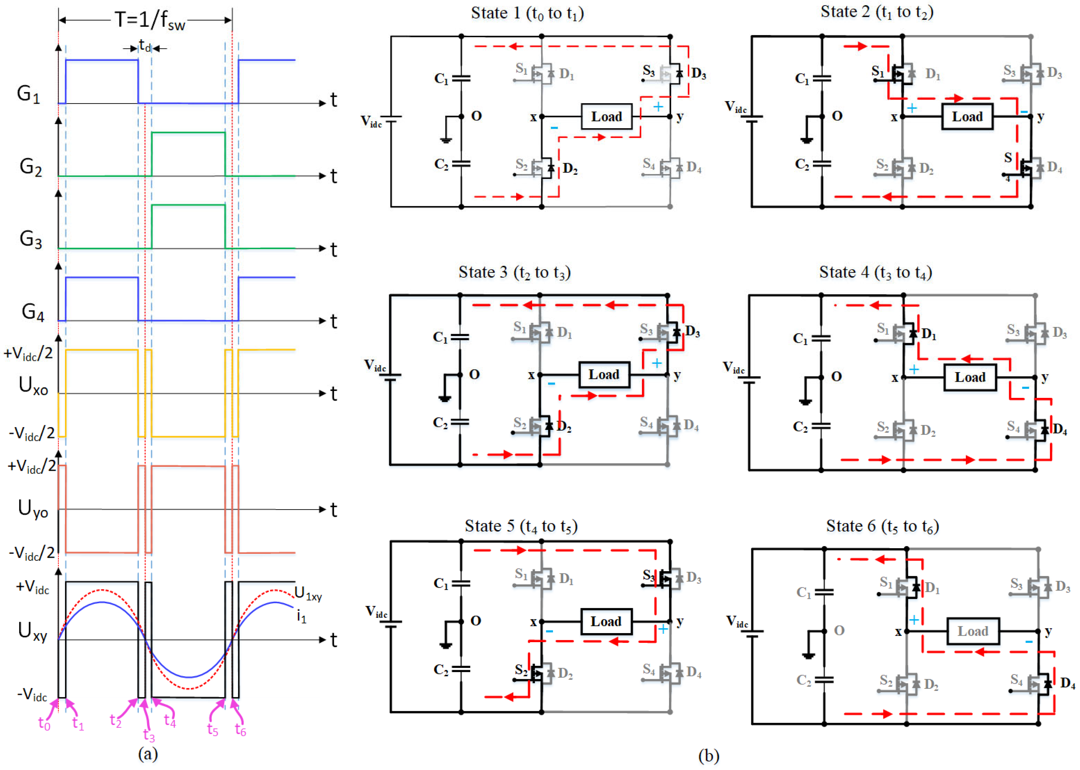
Figure 1. Block diagram of WPT charger for EV.
Sustainability 16 07045 g001
Figure 2. LCC-LCL compensation WPT circuit schematic.
Sustainability 16 07045 g002
Figure 3. Equivalent high-frequency inverter circuit schematic of WPT as a H-bridge inverter.
Sustainability 16 07045 g003
Figure 4. Concept waveform of PWM and PDM (a) without dead-time and (b) with dead-time.
Sustainability 16 07045 g004
Figure 5. PDM generating logic diagram.
Sustainability 16 07045 g005
Figure 6. (a) Operational waveforms of WPT system without the delay time; (b) current flow diagram for different states of WPT system.
Sustainability 16 07045 g006
Figure 7. (a) Operational waveforms of WPT system considering ϕ = α ≥ 0 with the dead time and (b) operational states of WPT system with current flow.
Sustainability 16 07045 g007
Figure 8. Formal output waveforms of the full bridge inverter when notch occurs.
Sustainability 16 07045 g008
Figure 9. Comparison of harmonics f = 85 kHz, for PWM and PDM (with different pulse density d = 0.2, 0.5, 0.8) (a) without dead time and (b) with dead time.
Sustainability 16 07045 g009
Figure 10. Equivalent circuit of a magnetic resonance wireless charger with LCC-LCL compensation topology.
Sustainability 16 07045 g010
Figure 11. Experimental arrangements of WPT with Spartan 6.
Sustainability 16 07045 g011
Figure 12. Simulation output wave forms of HF inverter WPT with PWM control for without dead time and with different dead times (500 ms, 1000 ms, 1500 ms, and 2000 ms).
Sustainability 16 07045 g012
Figure 13. Simulation output wave forms of HF inverter WPT with PDM (D = 0.2) control for without dead time and with different dead times (500 ms, 1000 ms, 1500 ms, and 2000 ms).
Sustainability 16 07045 g013
Figure 14. Simulation output wave forms of HF inverter WPT with PDM (D = 0.5) control for without dead time and with different dead times (500 ms, 1000 ms, 1500 ms, and 2000 ms).
Sustainability 16 07045 g014
Figure 15. Simulation output wave forms of HF inverter WPT with PDM (d = 0.8) control for without dead time and with different dead times (0.5 µs,1.0 µs,1.5 µs, 2.0 µs).
Sustainability 16 07045 g015
Figure 16. Graphical result analysis of WPT output parameters: (a) input DC voltage gain, (b) input DC voltage gain, (c) input AC voltage gain, (d) transconductance, (e) input DC power, (f) output DC load power, (g) receiver output power, and (h) receiver output power.
Sustainability 16 07045 g016
Figure 17. (a) Experimental result of PWM-controlled HF inverter voltage and current without dead time; (b) switching pulse of PWM 50% duty cycle.
Sustainability 16 07045 g017
Figure 18. Experimental results of HF inverter voltages and current with PWM control for different dead times: (a) td = 0.5 μs and (b) td = 1.0 μs. (c) td = 1.5 μs and (d) td = 2.0 μs.
Sustainability 16 07045 g018
Figure 19. Experimental output of PDM HF inverter voltage and current without dead time; (a) Inverter Voltage and Current (b) Switching Pulses D = 0.5 (c). Inverter Voltage and Current PDM of D = 0.5 (d). PDM of D = 0.5 (e). Inverter Voltage and Current PDM of D = 0.8 (f) Switching Pulses D = 0.8.
Sustainability 16 07045 g019
Figure 20. Experimental results of HF inverter voltages and current with PDM of d = 0.2 control for different dead times: (a) td = 0.5 μs and (b) td = 1.0 μs. (c) td = 1.5 μs and (d) td = 2.0 μs.
Sustainability 16 07045 g020
Figure 21. Experimental results of HF inverter voltages and current with PDM of d = 0.5 control for different dead times: (a) td = 0.5 μs and (b) td = 1.0 μs. (c) td = 1.5 μs and (d) td = 2.0 μs.
Sustainability 16 07045 g021aSustainability 16 07045 g021b
Figure 22. Experimental results of HF inverter voltages and current with PDM of d = 0.8 control for different dead-times: (a) td = 0.5 μs and (b) td = 1.0 μs. (c) td = 1.5 μs and (d) td = 2.0 μs.
Sustainability 16 07045 g022
Figure 23. The comparison experimental and simulation output current ripple with effect of different dead times for different PDM and PWM control.
Sustainability 16 07045 g023
Table 1. Switch transition table for without dead time.
Transition StateSwitch ConditionCurrent FlowOutput Voltage
State 1 (t0–t1)S1, S4-ON & S2, S3-OFF(+) Vidc-S1-Loadx-Loady-S4-(−) VidcUxy = +Vidc.
State 2 (t1–t2)S1, S4-OFF & S2, S3-OFF(+) Vidc-S3-Loady-Loadx-S2-(−) VidcUxy = −Vidc.
Table 2. Switch transition table for with dead time.
Transition StateSwitch ConditionCurrent FlowOutput Voltage
State 1 (t0–t1)S1, S2, S3, S4-OFF(−) Vidc-D2-Loadx-Loady-D3-(+) VidcUxy = −Vidc.
State 2 (t1–t2)S1, S4-ON & S2, S3-OFF(+) Vidc-S1-Loadx-Loady-S4-(−) VidcUxy = +Vidc.
State 3 (t2–t3)S1, S2, S3, S4-OFF(−) Vidc-D2-Loadx-Loady-D3-(+) VidcUxy = −Vidc.
State 4 (t3–t4)S1, S2, S3, S4-OFF(−) Vidc-D4-Loady-Loadx-D1-(+) VidcUxy = +Vidc.
State 5 (t4–t5)S1, S4-OFF & S2, S3-ON(+) Vidc-S3-Loady-Loadx-S2-(−) VidcUxy = −Vidc.
State 6 (t5–t6)S1, S2, S3, S4-OFF(−) Vidc-D4-Loady-Loadx-D1-(+) VidcUxy = +Vidc.
Table 3. LCC-LCL resonant compensation design parameters values.
SymbolDesigned Value
Lt74.56 µH
Ct15.05 nF
Ct26.26 nF
Lr36.3 µH
Cr10.05 nF
Table 4. Design parameters values of WPT.
ParameterLabelValue
Input DC voltage Primary coilVidc325 V
Transmitter coil self-InductanceL174.56 µH
Mutual inductanceLM15.95 µH
Receiver coil self-inductanceL285.45 µH
Output equivalent resistanceRload22 Ω
Output filter capacitanceCo22 µF
Operating switching frequencyfsw85,000 Hz
Coupling coefficientk0.2
Distance between transmitter to receiver coild180 mm
Table 5. Performance parameters values of WPT.
ParametersControl TechniqueWithout Dead TimeDead Time in (%)
15101520
Power dissipationPWM0.4000.9551.1451.3951.5001.555
PDM (D = 0.5)0.3420.4811.1301.3651.4251.470
PDM (D = 0.8)0.3000.7001.2451.2201.3251.540
Transfer efficiencyPWM86.1%84.3%89.7%93.8%95.5%96.8%
PDM (D = 0.5)86.7%84.4%89.2%92.7%94.1%98.4%
PDM (D = 0.8)80.7%81.3%82.2%82.8%84.2%84.4%
Overall efficiencyPWM88.4%85.5%62.2%50.8%46.4%30.3%
PDM (D = 0.5)90.2%88.3%63.6%55.8%52.3%37.6%
PDM (D = 0.8)92.2%89.4%66.3%64.2%61.1%50.4%
Color scaleLowest----Highest
Table 6. Performance values comparison of PWM and PDM control techniques in HF inverters of WPT with and without dead time.
Control TechniqueHF Inverter Voltage GainCurrent Ripple RatioHF Inverter
Efficiency
Without dead timePWM [36]1.252.5089.5
PDM [42]1.301.8090.2
With dead time (1 µs)PWM1.062.0586.5
PDM (0.5)1.191.9686.7
PDM (0.8)1.251.9589.5
Disclaimer/Publisher’s Note: The statements, opinions and data contained in all publications are solely those of the individual author(s) and contributor(s) and not of MDPI and/or the editor(s). MDPI and/or the editor(s) disclaim responsibility for any injury to people or property resulting from any ideas, methods, instructions or products referred to in the content.

