Article

An Effective Transformerless PUC7-Based Dynamic Voltage Restorer Using Model Predictive Control

1
Electronics and Communications Engineering Department, Kuwait College of Science and Technology, Kuwait City P.O. Box 27235, Kuwait
2
Department of Computer Engineering, Eastern Mediterranean University, Via Mersin 10, Famagusta 999043, Turkey
3
Qatar Environment and Energy Research Institute, Hamad Bin Khalifa University, Doha P.O. Box 34110, Qatar
4
Department of Electrical and Computer Engineering, Texas A&M University at Qatar, Qatar Foundation, Doha P.O. Box 23874, Qatar
*
Authors to whom correspondence should be addressed.
Sustainability 2023, 15(4), 3041; https://doi.org/10.3390/su15043041
Submission received: 14 December 2022 / Revised: 24 January 2023 / Accepted: 24 January 2023 / Published: 7 February 2023

Abstract

:
This paper investigates the performance of a seven-level Packed U Cell (PUC7) inverter-based transformerless Dynamic Voltage Restorer (DVR) topology under short-time voltage variations (voltage sags and swells). Unlike the existing multilevel inverter (MLI)-based DVR solutions, the proposed structure requires only one DC voltage source (suitable for PV-based DVR systems), one capacitor, and six switching devices to generate seven-level output voltage. Moreover, the studied topology is characterized by reduced cost and size due to the elimination of the injection transformer. The PUC7 inverter is controlled using a multi-objective (filtering current, compensating voltage, and PUC capacitor voltage controls) Model Predictive Control (MPC) strategy. Simulation and implementation tests are carried out to demonstrate the high performance of the proposed DVR at steady-state and during transient conditions, while keeping the load voltage unaffected by the disturbances in the grid voltage.

1. Introduction

Currently, renewable energy (RE) is significantly and progressively attracting attention worldwide. RE involves natural energy sources that deliver electrical power without emitting greenhouse gases. Such sources have been used to guarantee power delivery to remote locations without making changes to transmission/distribution networks (standalone applications) and/or to provide support to the utility in case of failures (grid-connected applications). Thus, RE has become a priority in the energy sector for many countries. Photovoltaic (PV) energy has recently shown the highest investment potential among RE. In this regard, the demand for PV has been growing steadily at a pace of almost 25% per year over the past two decades, particularly for grid-tied applications. This accelerating development is associated with significant and challenging requirements for power conversion such as flexibility, reliability, modularity, performance, and quality [1].
Moreover, loads connected at the point of common coupling (PCC) are subject to voltage sags/swells occurring in the utility system. These short-time voltage variations can easily halt the operation of industrial and domestic equipment causing unplanned equipment failures and shutdowns. Therefore, reliable/high-quality power delivery at the PCC is an indispensable requirement [2]. Dynamic voltage restorers (DVRs) are widely employed in series with the grid voltage to inject the needed compensation to maintain the voltage of the load at the required level during voltage sags/swells. A basic DVR consists of a DC power supply, an inverter, a filter, and a transformer [3,4,5,6,7,8,9]. Thus, the use of PV as a clean power supply appears to be an obvious choice in DVR systems to target an effective compensation and keep the load voltage unaltered from grid voltage disturbances.
Many power electronic converter configurations have already been used for DVR applications. In [10,11], the DC input voltage of the voltage source inverter (VSI) is obtained from the AC utility voltage using a controlled three-phase rectifier. Many transformerless DVR topologies were presented in [12,13,14,15] where the compensating voltage is injected using a series connected capacitor. Transformerless DVR is suitable for use in residential environments due to its reduced volume. Furthermore, multilevel inverter (MLI)-based DVR topologies with the aim of improving the load voltage quality are also widely studied [16,17,18,19,20,21,22,23,24]. The cascaded H-bridge inverter-based DVR topologies proposed in [16,17] can be connected to PCC without a transformer, but require isolated DC source for each H-bridge inverter. In addition, three H-bridge inverters are necessary to achieve a seven-level load voltage, requiring 12 bidirectional switching devices. In [18], the application of a transformer-coupled cascaded H-bridge inverter-based DVR requiring only one DC source is investigated. In [19,20], flying capacitor inverter (FCI)-based DVR topology is introduced. In general, an FCI with M levels requires M-1 pairs of switching devices and M-2 flying capacitors. Hence, for a seven-level load voltage, FCI based DVR topology requires 12 switching devices and five flying capacitors. However, the FCI topology is characterized by an easier extension for higher voltage levels compared to neutral point clamped (NPC) inverter topology [20,21]. Different from FCI and NPC, other MLI-based topologies have been studied in the literature such as stacked multicell [23] and T-type inverters [23]. The common drawback of the aforementioned topologies is the exponential increase in the number of active/passive elements for higher voltage levels.
In this paper, the feasibility of a transformerless PV-based DVR topology [25] employing a seven-level packed U cell (PUC7) inverter is investigated. PUC inverters are single-DC-source MLI topologies (SDCS-MLI) characterized by their ability to generate higher output voltage levels with a single DC supply and their control flexibility, taking advantage of the redundant switching states. PUC topology outperforms most existing SDCS-MLIs in terms of reliability, high voltage ride through capability (capacitors as storage elements), and reduced cost (less number of switching devices) [26,27,28,29]. Unlike existing MLI-based DVRs, the proposed system requires only one DC source, one capacitor, and six switching devices. Table 1 presents a comparison between the existing most common MLI-based DVR solutions.
To inject a compensating voltage with appropriate amplitude and phase angle (comparison of the desired load voltage and the measured line voltage), a suitable control strategy should be applied to the PUC-based DVR. Therefore, a model predictive control (MPC) approach is proposed in this paper to control the compensating voltage, the filtering current, and the capacitor voltage of the PUC topology. A cost function regrouping the control objectives is minimized to select the optimal switching state at each sampling time.
The paper is structured as follows: The topology and modeling of the proposed DVR are discussed in Section 2. Section 3 details the MPC design, while Section 4 presents and discusses the simulation and implementation results. Finally, Section 5 concludes the paper.

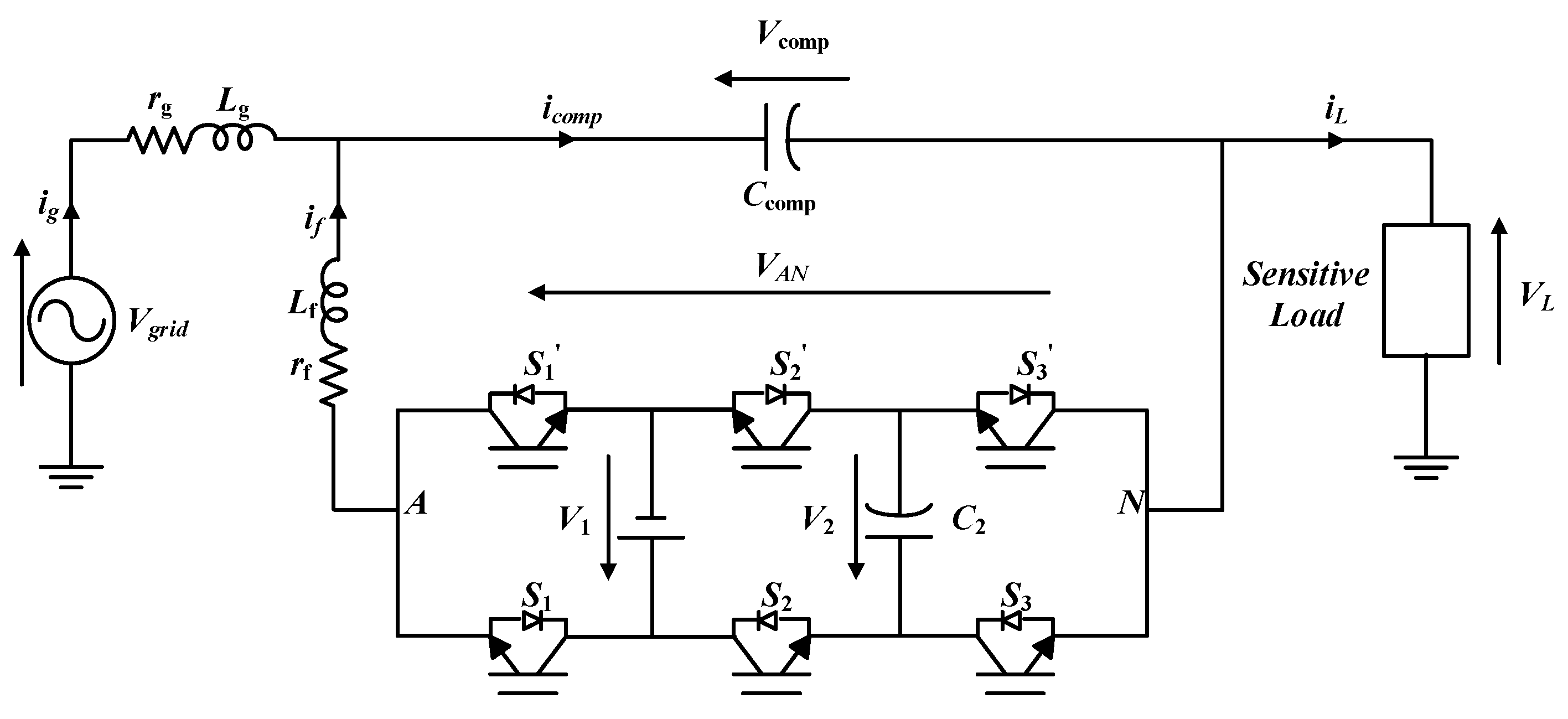
2. PUC-Based DVR Topology and Modeling

2.1. Topology

The seven-level PUC structure is built by cascading three cells, where each of the cells is created by encompassing one capacitor/DC voltage source by two switches (controlled in a complimentary manner). It is worth noting that the voltage V2 across the capacitor C2 should be regulated at 1/3 of the DC input voltage V1 (V2* = V1/3). Figure 1 shows the proposed transformerless PUC-based DVR topology. The compensating voltage (Vcomp) is injected to the system via series-connected capacitor Ccomp. It is obvious that this topology does not require an injection transformer which reduces the cost and volume of the DVR.
The switching patterns (Si denotes the switching state of the switch i = 1…3 while Si denotes the switching state of the complementary switch) and the corresponding generated levels of the output voltage are illustrated in Table 2.

2.2. Modeling

The state variables are selected to be (i) the compensating voltage Vcomp(t), (ii) the filtering current if(t), and (iii) the PUC capacitor voltage V2(t). Applying Kirchhoff’s current and voltage laws, the first order differential equations related to the selected three state variables are given by:
C c o m p d V c o m p ( t ) d t = i f ( t ) + i g ( t )
C 2 d V 2 ( t ) d t = ( S 3 S 2 ) i f ( t )
L f d i f ( t ) d t = V A N ( t ) V c o m p ( t ) r f i f ( t )

3. MPC Design

A multi-objective finite control set MPC (FCS-MPC) is applied to the studied DVR system. The compensating voltage Vcomp(k + 1), the filtering current if(k + 1), and the PUC capacitor voltage V2(k + 1) are predicted for the different switching configurations. Thus, the aforementioned state equations can be approximated at each sampling time Ts using the Taylor expansion given in (4) by Equations (5)–(7).
x ( k + 1 ) x ( k ) + x ˙ ( t ) . T s
V c o m p ( k + 1 ) = V c o m p ( k ) + T s C c o m p ( i f ( k ) + i g ( k ) )
V 2 ( k + 1 ) = V 2 ( k ) + T s C 2 ( S 3 S 2 ) i f ( k )
i f ( k + 1 ) = i f ( k ) ( 1 r f L f T s ) + T s L f ( V A N ( k ) V c o m p ( k ) )
Figure 2 shows the general view of the proposed MPC approach. The tracking errors are computed from the desired values and the predicted state variables for the eight switching configurations, and then incorporated into the cost function g given by Equation (8). Next, the switching pattern that minimizes g is chosen and applied to the converter during the next sampling time. It is worth mentioning that λcomp is used as a weighting factor to adjust the control priorities.
g = | V 2 * ( k + 1 ) V 2 ( k + 1 ) | + λ c o m p | V c o m p * ( k + 1 ) V c o m p ( k + 1 ) | + | i f * ( k + 1 ) i f ( k + 1 ) |
For the sake of simplicity, the reference values of the filtering current if*(k + 1) and the compensation voltage Vcomp*(k + 1) are supposed to be equal to those at (k) sampling time, which are calculated by:
i f * ( k ) = i c o m p ( k ) i L * ( k )
V c o m p * ( k ) = V L * ( k ) V g r i d ( k )
where the reference load current i L * ( k ) is computed using Ohm’s law from the reference load voltage V L * ( k ) .

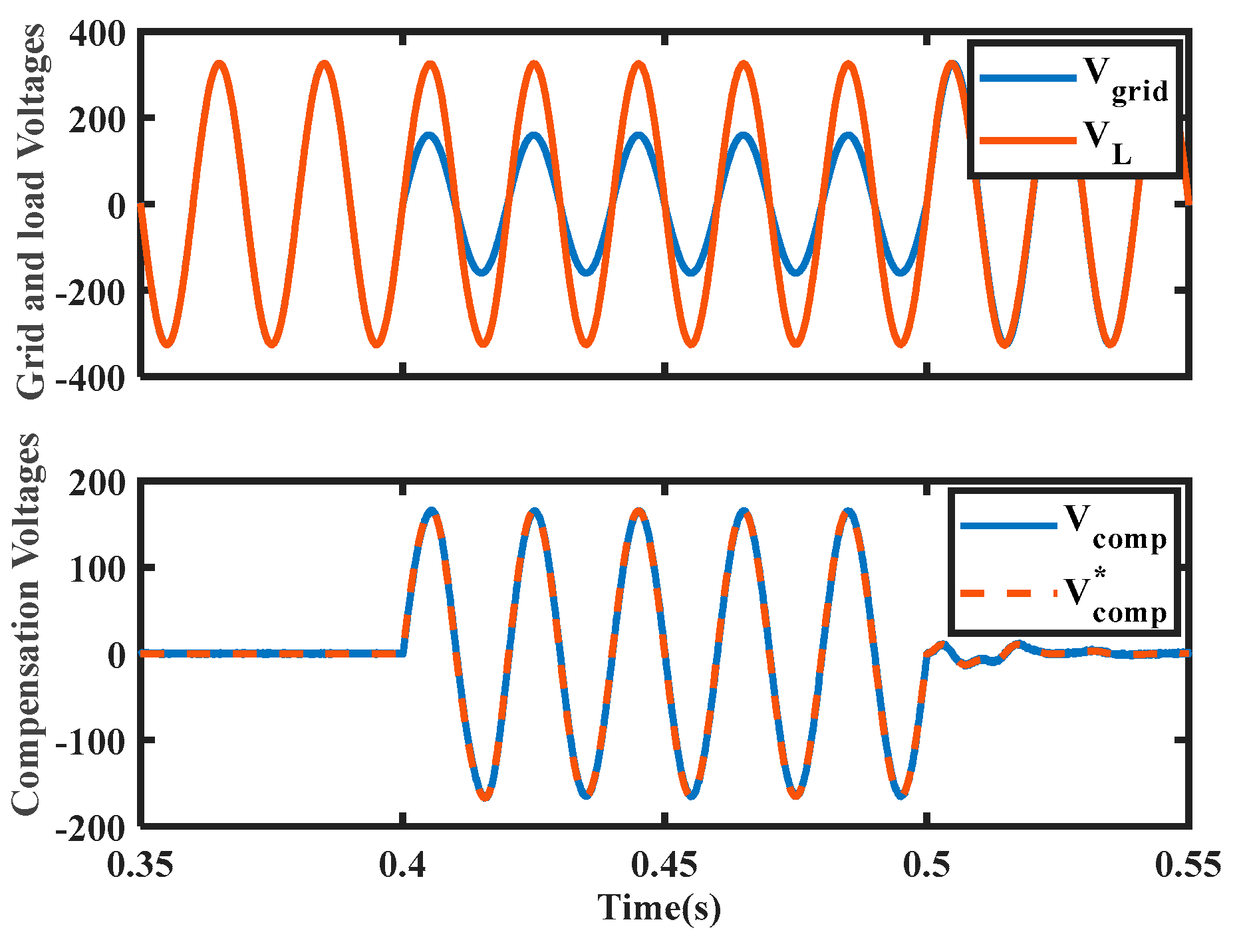
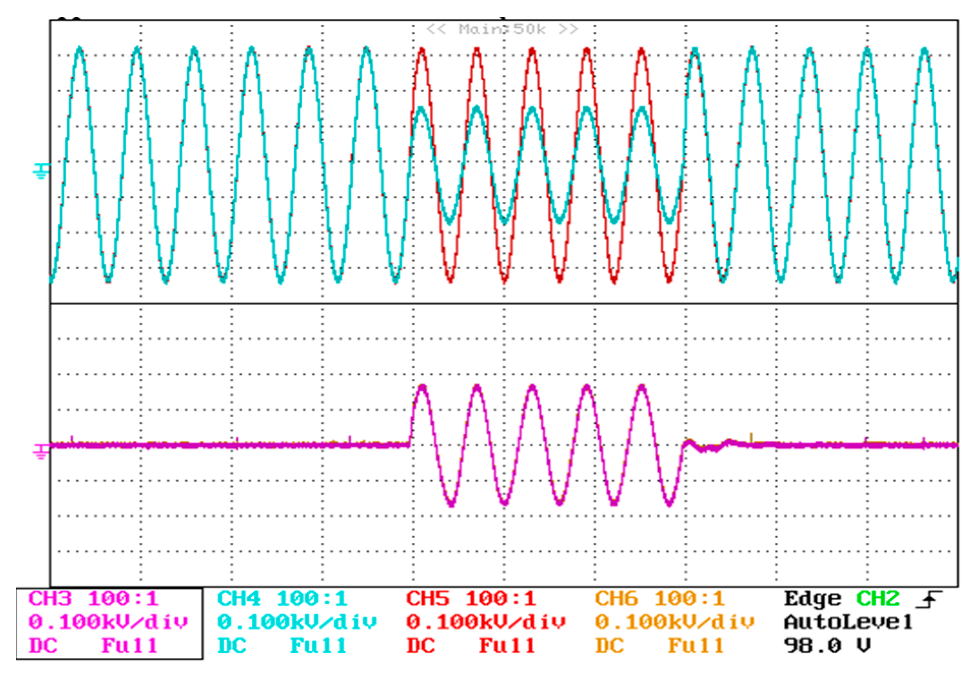
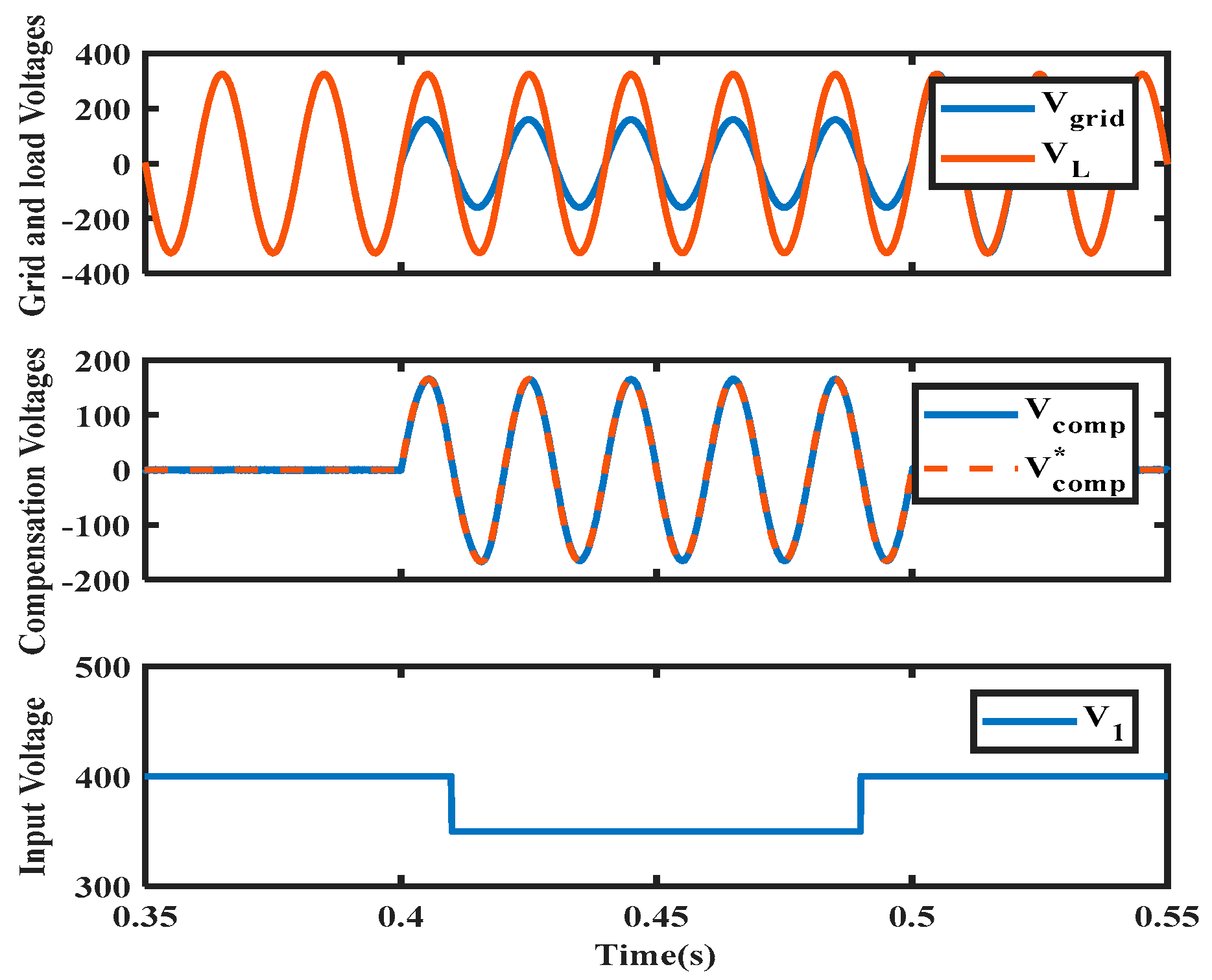
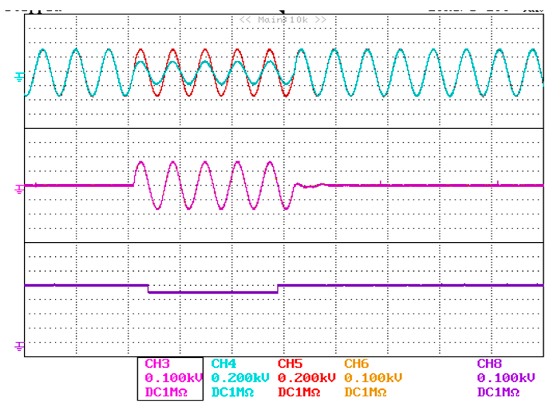
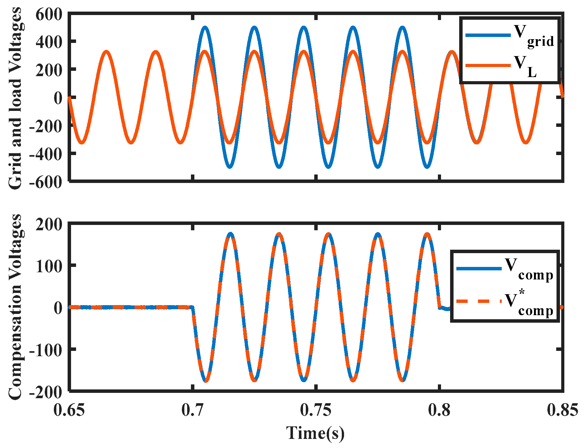
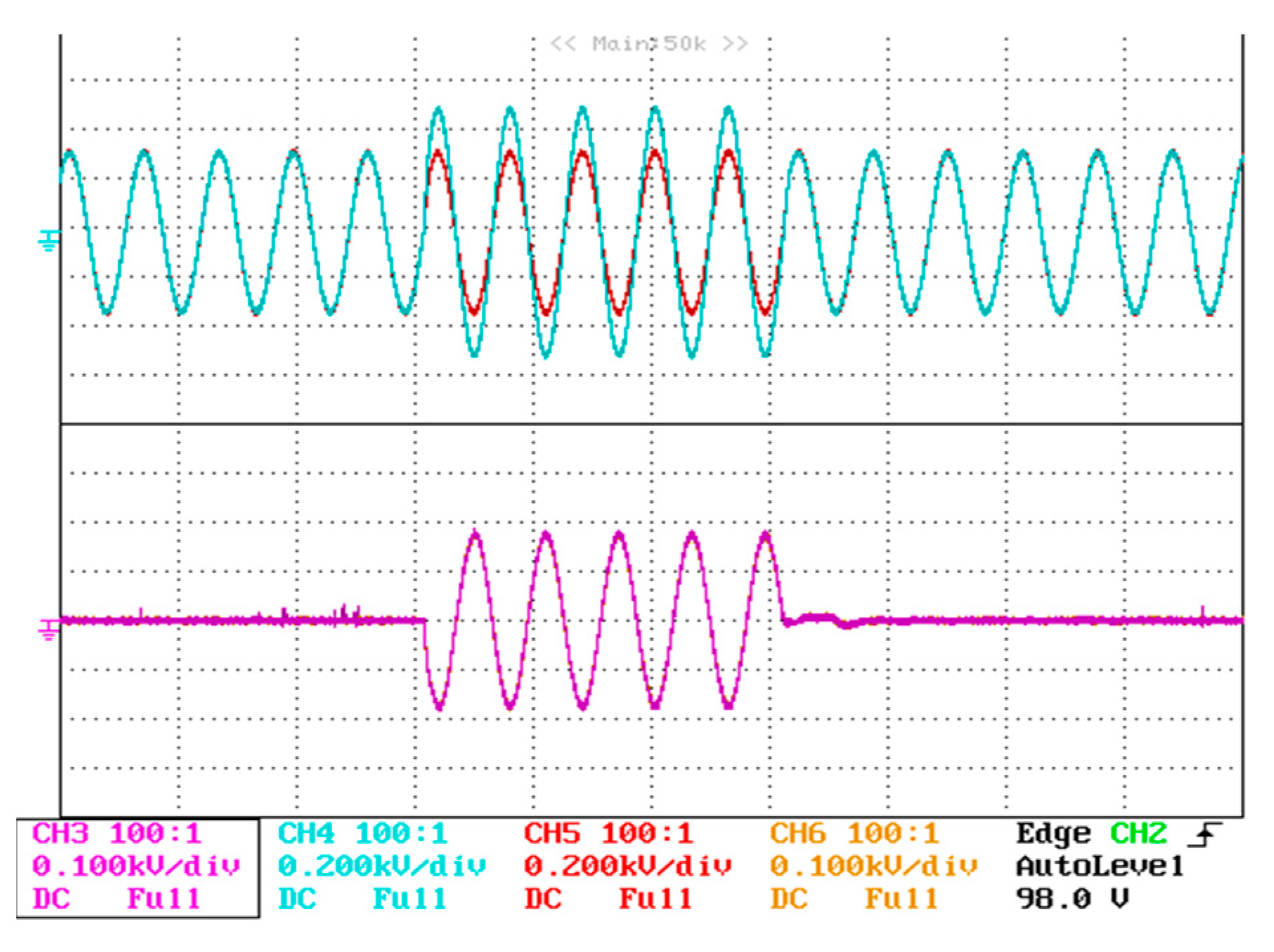
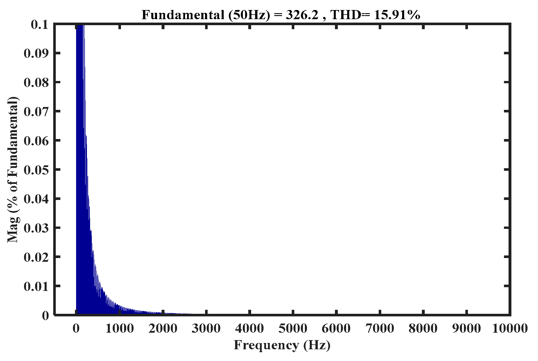
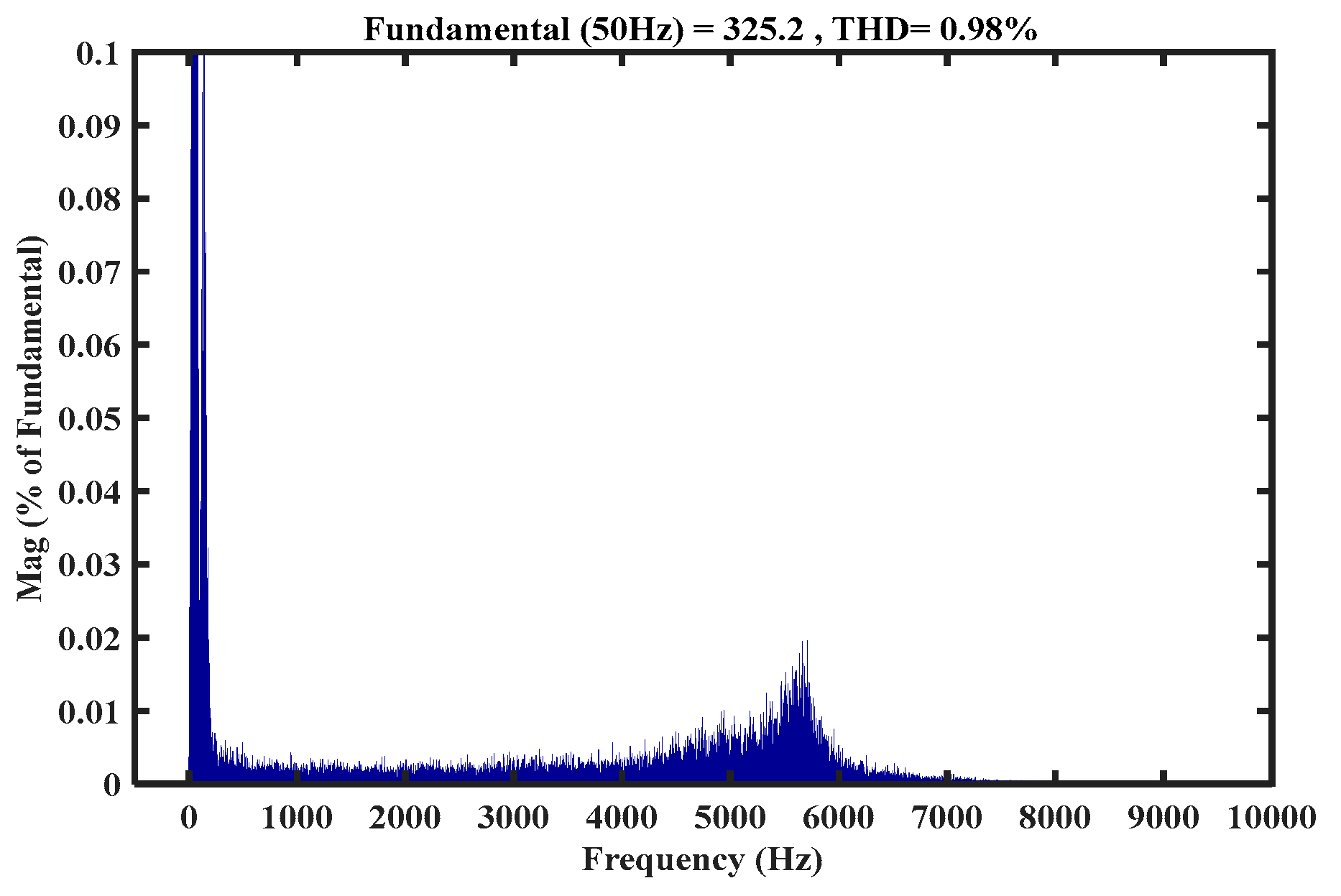
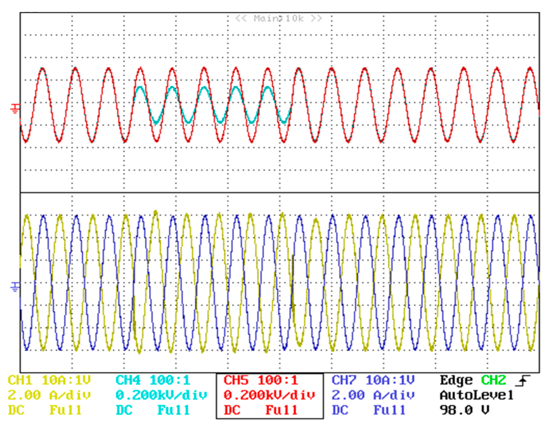
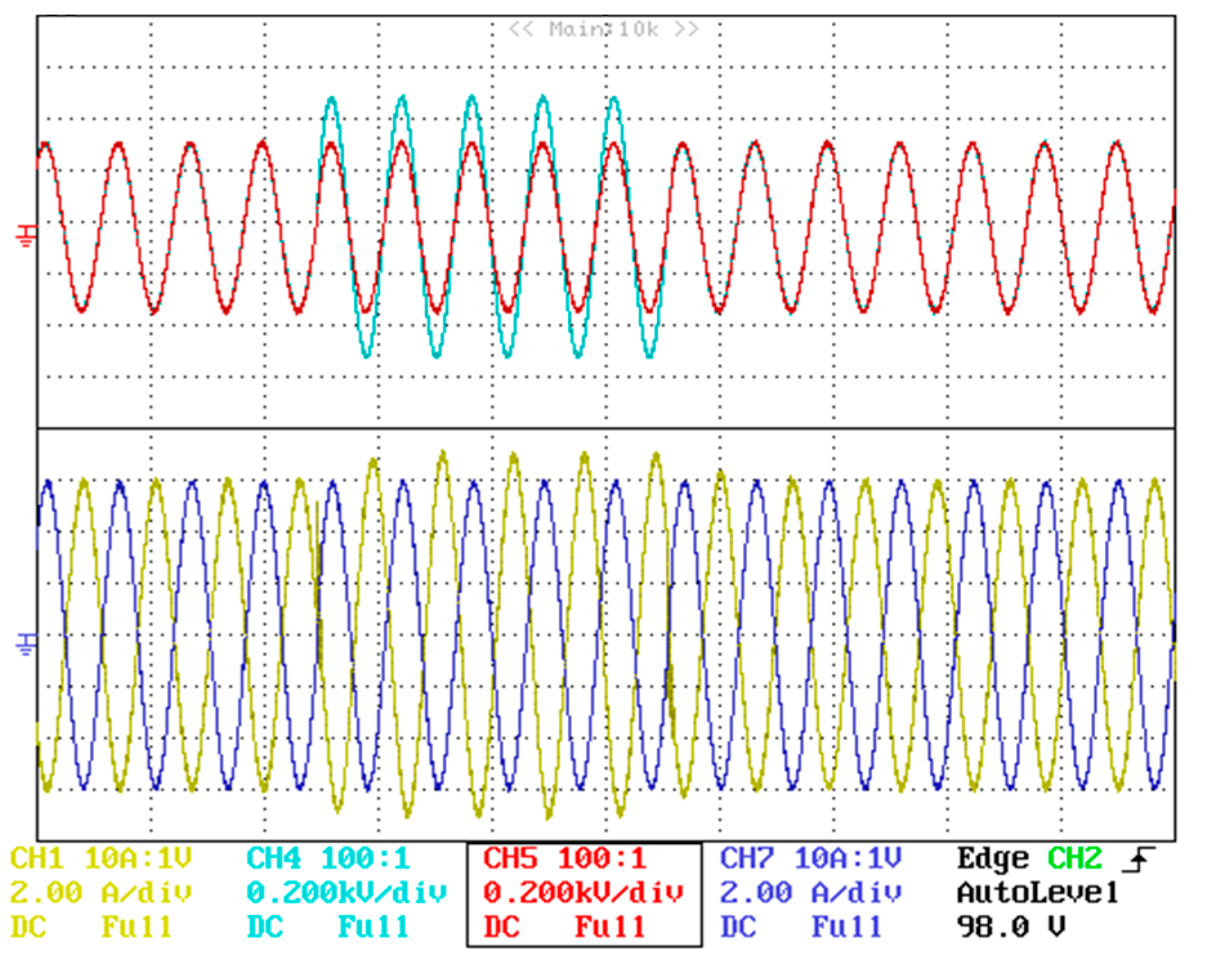
4. Simulation and Real-Time Implementation Results

A Matlab/Simulink environment is used in this paper to simulate the proposed DVR system. Moreover, a dSpace 1103 controller board is employed to enable the dynamic real-time simulation responses and validate the results. The system parameters used in both simulation and real-time validations are illustrated in Table 3, while the setup of the system’s real-time implementation is shown in Figure 3.
To verify the effectiveness of the proposed system, several tests were performed by introducing line voltage dips and swells. Figure 4 and Figure 5 show the simulation and implementation results of the line voltage, compensation voltage, and load voltage during a short period of decrease in the rms value of the line voltage (five cycles voltage dip). The produced compensating voltage remains null before the line voltage drops. When the voltage sag occurs, the required compensating voltage is generated to maintain the sensitive load voltage at the required level.
Moreover, the ability of the proposed DVR to mitigate the voltage drops when the input voltage changes (a step-down change from 400 V to 350 V) is illustrated in Figure 6 and Figure 7.
Another test was performed by emulating a grid voltage swell. The corresponding simulation and implementation results are presented in Figure 8 and Figure 9. One can notice that the proposed PUC-based DVR system injects a compensating voltage with 180° phase shift compared to the line voltage to keep the load voltage unaffected.
Figure 10 and Figure 11 show the FFT spectrums of the grid and load voltages with the respective voltage THD values. One can notice that Figure 11 confirms the effectiveness of the proposed PUC7-based DVR solution in protecting the load voltage (voltage THD around 1%) against the grid voltage disturbances (voltage grid THD around 15% during voltage sag/swell operating conditions as depicted by Figure 10). This reduced voltage THD at the load side is due to the produced multilevel output voltage (seven-level output voltage) at the inverter side.
The dynamics of the different currents flowing in the proposed DVR system (load current, compensation current, and filtering current) during line voltage sag/swell events are illustrated in Figure 12, Figure 13, Figure 14 and Figure 15. Obviously, during normal operating conditions, no current will be flowing across the compensation capacitor. As a result, the filtering current is 180° phase shifted from the load current (if = −iL). At the voltage sag/swell events, a compensating sinusoidal current is produced to make icomp = iL + if.

5. Conclusions

This paper proposed a transformerless Packed U Cell (PUC)-based dynamic voltage restorer (DVR) solution for single-phase PV systems. The investigated topology is characterized by its lowered cost and size due to the exclusion of the injection transformer. The aim of the proposed system is to produce a compensation voltage during grid voltage sag/swell events to keep the load voltage unaffected. An effective finite control set model predictive control (FCS-MPC) strategy was proposed to ensure the generation of the required compensating voltage while regulating the filtering current and the PUC capacitor voltage around their references throughout the line voltage disturbances. Theoretical study, simulation, and real-time implementation results were presented, during normal and disturbed operating conditions, to demonstrate the high dynamic performance and the effectiveness of the proposed solution. However, the computational burden remains a challenge for FCS-MPC techniques due to the real-time calculation constraints. Another emerging research axis concerns the tuning of the weighting factors to sort the priorities of the control objectives in the control decision. Artificial intelligence-based algorithms could play an important role in the auto-tuning process of the weighting factors and deal with the codependency of the control objectives.

Author Contributions

Conceptualization, M.T. and H.K.; formal analysis, M.T., H.K., S.B. and H.A.-R.; investigation, M.T.; methodology, M.T. and H.K.; supervision, H.A.-R.; validation, M.T., H.K., S.B. and H.A.-R.; writing—original draft, M.T.; writing—review & editing, M.T., H.K., S.B. and H.A.-R. All authors have read and agreed to the published version of the manuscript.

Funding

This publication was made possible by NPRP12C-33905-SP-213 from the Qatar National Research Fund (a member of Qatar Foundation). The statements made herein are the sole responsibility of the authors.

Institutional Review Board Statement

Not applicable.

Informed Consent Statement

Not applicable.

Data Availability Statement

Not applicable.

Conflicts of Interest

The authors declare no conflict of interest.

References

  1. Twidell, J.; Weir, T. Renewable Energy Resources, 3rd ed.; Routledge: London, UK, 2015. [Google Scholar] [CrossRef]
  2. Bollen, M. Understanding Power Quality Problems, Voltage Sags and Interruptions; IEEE Press: Piscataway, NJ, USA, 2000. [Google Scholar]
  3. Li, Y.W.; Blaabjerg, F.; Vilathgamuwa, D.M.; Loh, P.C. Design and comparison of high performance stationary-frame controllers for DVR implementation. IEEE Trans. Power Electron. 2007, 22, 602–612. [Google Scholar] [CrossRef]
  4. Li, Y.W.; Vilathgamuwa, D.M.; Blaabjerg, F.; Loh, P.C. A robust control scheme for medium-voltage-level DVR implementation. IEEE Trans. Ind. Electron. 2007, 54, 2249–2261. [Google Scholar]
  5. Biricik, S.; Komurcugil, H. Optimized sliding mode control to maximize existence region for single-phase dynamic voltage restorers. IEEE Trans. Ind. Inform. 2012, 12, 1486–1497. [Google Scholar] [CrossRef]
  6. Naidu, T.A.; Arya, S.R.; Maurya, R. Multi-objective dynamic voltage restorer with modified EPLL control and optimized PI controller gains. IEEE Trans. Power Electron. 2018, 34, 2181–2192. [Google Scholar] [CrossRef]
  7. Li, P.; Xie, L.; Han, J.; Pang, S.; Li, P. A new voltage compensation philosophy for dynamic voltage restorer to mitigate voltage sags using three-phase voltage ellipse parameters. IEEE Trans. Power Electron. 2018, 33, 1154–1166. [Google Scholar] [CrossRef]
  8. Torres, A.P.; Sanchez, P.R.; Batlle, V.F. A two degree of freedom resonant control scheme for voltage-sag compensation in dynamic voltage restorers. IEEE Trans. Power Electron. 2018, 33, 4852–4867. [Google Scholar] [CrossRef]
  9. Pradhan, M.; Mishra, M.K. Dual P-Q theory based energy optimized dynamic voltage restorer for power quality improvement in distribution system. IEEE Trans. Ind. Electron. 2018, 66, 2946–2955. [Google Scholar] [CrossRef]
  10. Babaei, E.; Kangarlu, M.F. Voltage quality improvement by a dynamic voltage restorer based on a direct three-phase converter with fictitious DC link. IET Gener. Transm. Distrib. 2011, 5, 814–823. [Google Scholar] [CrossRef]
  11. Ebrahimzadeh, E.; Farhangi, S.; Iman-Eini, H.; Ajaei, F.B.; Iravani, R. Improved phasor estimation method for dynmaic voltage restorer applications. IEEE Trans. Power Deliv. 2015, 30, 1467–1477. [Google Scholar] [CrossRef]
  12. Li, B.H.; Choi, S.S.; Vilathgamuwa, D.M. Transformerless dynamic voltage restorer. IEE Gener. Transm. Distrib. 2002, 149, 263–273. [Google Scholar] [CrossRef]
  13. Sng, E.K.K.; Choi, S.S.; Vilathgamuwa, D.M. Analysis of series compensation and DC-link voltage controls of a transformerless self-charging dynamic voltage restorer. IEEE Trans. Power Deliv. 2004, 19, 1511–1518. [Google Scholar] [CrossRef]
  14. Kumar, C.; Mishra, M.K. Predictive voltage control of transformerless dynamic voltage restorer. IEEE Trans. Ind. Electron. 2015, 62, 2693–2697. [Google Scholar] [CrossRef]
  15. Komurcugil, H.; Biricik, S. Time-varying and constant switching frequency-based sliding-mode control methods for transformerless DVR employing half-bridge VSI. IEEE Trans. Ind. Electron. 2017, 64, 2570–2579. [Google Scholar] [CrossRef]
  16. Loh, P.C.; Vilathgamuwa, D.M.; Tang, S.K.; Long, H.L. Multilevel dynamic voltage restorer. IEEE Power Electron. Lett. 2004, 2, 125–130. [Google Scholar] [CrossRef]
  17. Shahabadini, M.; Iman-Eini, H. Improving the Performance of a Cascaded H-Bridge-Based Interline Dynamic Voltage Restorer. IEEE Trans. Power Deliv. 2016, 31, 1160–1167. [Google Scholar] [CrossRef]
  18. Wang, B.; Venkataramanan, G.; Illindala, M. Operation and control of a dynamic voltage restorer using transformer coupled H-bridge converters. IEEE Trans. Power Electron. 2006, 21, 1053–1061. [Google Scholar] [CrossRef]
  19. Roncero-Sanchez, P.; Acha, E. Dynamic voltage restorer based on flying capacitor multilevel converters operated by repetitive control. IEEE Trans. Power Del. 2009, 24, 951–960. [Google Scholar] [CrossRef]
  20. Khoshkbar-Sadigh, A.; Farzamkia, S.; Dargahi, V. Dynamic Voltage Restorer Controlled with Energy Minimized Compensation Method Based on Double Flying Capacitor Multicell Inverter. In Proceedings of the 2020 Clemson University Power Systems Conference (PSC), Clemson, SC, USA, 10–13 March 2020; pp. 1–5. [Google Scholar] [CrossRef]
  21. Tolbert, L.M.; Peng, F.Z.; Habetler, T.G. A multilevel converter-based universal power conditioner. IEEE Trans. Ind. Appl. 2000, 36, 596–603. [Google Scholar] [CrossRef]
  22. Barros, J.D.; Silva, J.F. Multilevel optimal predictive dynamic voltage restorer. IEEE Trans. Ind. Electron. 2010, 57, 2747–2760. [Google Scholar] [CrossRef]
  23. Khoshkbar Sadigh, A.; Babaei, E.; Hosseini, S.H.; Farasat, M. Dynamic voltage restorer based on stacked multicell converter. In Proceedings of the IEEE International Symposium on Industrial Electronics and Application (ISIEA2009), Kuala Lumpur, Malaysia, 4–6 October 2009; pp. 419–424. [Google Scholar]
  24. Komurcugil, H.; Bayhan, S.; Guler, N.; Abu-Rub, H.; Bagheri, F. A simplified sliding-mode control method for multi-level transformerless DVR. IET Power Electron. 2022, 15, 764–774. [Google Scholar] [CrossRef]
  25. Trabelsi, M.; Komurcugil, H.; Refaat, S.S.; Abu-Rub, H. Model predictive control of packed U cells based transformerless single-phase dynamic voltage restorer. In Proceedings of the 19th IEEE International Conference on Industrial Technology (ICIT2018), Lyon, France, 20–22 February 2018; pp. 1926–1931. [Google Scholar]
  26. Ounejjar, Y.; Al-Haddad, K.; Gregoire, L.A. Packed U cells multilevel converter topology: Theoretical study and experimental validation. IEEE Trans. Ind. Electron. 2011, 58, 1294–1306. [Google Scholar] [CrossRef]
  27. Vahedi, H.; Al-Haddad, K. Real-time implementation of a seven-level packed U-cell inverter with a low-switching-frequency voltage regulator. IEEE Trans. Power Electron. 2016, 31, 5967–5973. [Google Scholar] [CrossRef]
  28. Trabelsi, M.; Bayhan, S.; Ghazi, K.A.; Abu-Rub, H.; Ben-Brahim, L. Finite-Control-Set Model Predictive Control for Grid-Connected Packed-U-Cells Multilevel Inverter. IEEE Trans. Ind. Electron. 2016, 63, 7286–7295. [Google Scholar] [CrossRef]
  29. Vahedi, H.; Labbé, P.A.; Al-Haddad, K. Sensor-less five-level packed U-Cell (PUC5) inverter operating in standalone and grid-connected modes. IEEE Trans. Ind. Inform. 2016, 12, 361–370. [Google Scholar] [CrossRef]
Figure 1. The proposed transformerless PUC-based DVR.
Sustainability 15 03041 g001
Figure 2. Control synoptic of the proposed FCS-MPC strategy.
Sustainability 15 03041 g002
Figure 3. Setup of the proposed DVR solution.
Sustainability 15 03041 g003
Figure 4. Simulation results during line voltage sag; upper: grid and load voltages (Vgrid in blue and VL in red), lower: compensation voltage Vcomp.
Sustainability 15 03041 g004
Figure 5. Implementation results during line voltage sag; upper: grid and load voltages (Vgrid in blue and VL in red), lower: compensation voltage Vcomp.
Sustainability 15 03041 g005
Figure 6. Simulation results during line voltage sag and input voltage variation; upper: grid and load voltages (Vgrid in blue and VL in red), medium: compensation voltage Vcomp, lower: input voltage V1.
Sustainability 15 03041 g006
Figure 7. Implementation results during line voltage sag and input voltage variation; upper: grid and load voltages (Vgrid in blue and VL in red), medium: compensation voltage Vcomp, lower: input voltage V1.
Sustainability 15 03041 g007
Figure 8. Simulation results during line voltage swell; upper: grid and load voltages (Vgrid in blue and VL in red), lower: compensation voltage Vcomp.
Sustainability 15 03041 g008
Figure 9. Implementation results during line voltage swell; upper: grid and load voltages (Vgrid in blue and VL in red), lower: compensation voltage Vcomp.
Sustainability 15 03041 g009
Figure 10. FFT analysis and THD of the grid voltage in the presence of sag/swell events.
Sustainability 15 03041 g010
Figure 11. FFT analysis and THD of the load voltage in the presence of sag/swell events.
Sustainability 15 03041 g011
Figure 12. Simulation results of the current waveforms during line voltage sag; upper: filtering current if and load current iL, lower: the produced compensating current icomp.
Sustainability 15 03041 g012
Figure 13. Implementation results of the current waveforms during line voltage sag; upper: grid and load voltages (Vgrid in blue and VL in red), lower: filtering current if and load current iL.
Sustainability 15 03041 g013
Figure 14. Simulation results of the current waveforms during line voltage swell; upper: filtering current if and load current iL, lower: the produced compensating current icomp.
Sustainability 15 03041 g014
Figure 15. Implementation results of the current waveforms during line voltage swell; upper: grid and load voltages (Vgrid in blue and VL in red), lower: filtering current if and load current iL.
Sustainability 15 03041 g015
Table 1. Comparison between the existing most common MLI-based DVR solutions.
DVR TopologyAdvantagesDisadvantages
Two-level
Inverter
  • Easy implementation
  • Reduced cost
  • High switching frequency
  • High switching losses
  • Decreased efficiency
NPC Inverter
  • Easy implementation
  • Clamping diodes
  • Extra control to deal with the unbalance of the capacitor mid-point voltage
T-type Inverter
  • Lack of clamping diodes
  • Higher efficiency (NPC)
  • Lower cost (NPC)
  • Extra control to deal with the unbalance of the capacitor mid-point voltage
CHB Inverter
  • Reduced harmonic content
  • Multiple DC-source
  • High cost
FCI Inverter
  • Single DC-Source
  • Easy extension for higher voltage levels
  • Challenging control
  • High number of components
  • High cost
PUC Inverter
  • Minimum number of components
  • Single DC-Source
  • Easy extension for higher voltage levels
  • Reduced cost
  • Challenging control
Table 2. Switching patterns of the PUC7 inverter.
StateVANS1S2S3
10000
2V2001
3V2V1010
4V1011
5V1100
6V1V2101
7V2110
80111
Table 3. Parameters used for simulation and real-time implementations.
ParametersValues
AC grid RMS voltage (Vgrid)230 V
Input voltage (V1)400 V
Filter inductor (Lf)0.7 mH
Filter internal resistor (rf)0.5 Ω
Filter capacitor (Ccomp)50 μF
PUC capacitors (C1, C2)100 μF
Grid inducor (Lg)0.1 mH
Load inductor (LL)10 mH
Load resistor (RL)50 Ω
Sampling time (Ts)35 μs
Disclaimer/Publisher’s Note: The statements, opinions and data contained in all publications are solely those of the individual author(s) and contributor(s) and not of MDPI and/or the editor(s). MDPI and/or the editor(s) disclaim responsibility for any injury to people or property resulting from any ideas, methods, instructions or products referred to in the content.

