Article

Effect of Adding Cu2O as a Back Surface Field Layer on the Performance of Copper Manganese Tin Sulfide Solar Cells

1
Laboratory of Elaboration and Characterization Physico-Mechanical and Metallurgical of Materials (ECP3M), Université Abdelhamid Ibn Badis Mostaganem, Mostaganem 27000, Algeria
2
Laboratory of Analysis and Application of Radiation, Faculty of Physics, Université des Sciences et de la Technology d’Oran Mohamed Boudiaf, USTO-MB, Oran 31000, Algeria
3
Physics Department, Université Abdelhamid Ibn Badis Mostaganem, Mostaganem 27000, Algeria
4
College of Materials Science and Engineering, Donghua University, Shanghai 201620, China
5
College of Engineering, University of Warith Al-Anbiyaa, Karbala 56001, Iraq
6
Department of Chemistry, College of Sciences, King Khalid University, Abha P.O. Box 9004, Saudi Arabia
7
VLSI Centre of Excellence, Chitkara University Institute of Engineering and Technology, Chitkara University, Punjab 140401, India
8
Institute of Electronics, Atomic Energy Research Establishment, Bangladesh Atomic Energy Commission, Dhaka 1349, Bangladesh
9
Department of Advanced Energy Engineering Science, Interdisciplinary Graduate School of Engineering Sciences, Kyushu University, Fukuoka 816-8580, Japan
*
Author to whom correspondence should be addressed.
Sustainability 2023, 15(19), 14322; https://doi.org/10.3390/su151914322
Submission received: 29 August 2023 / Revised: 23 September 2023 / Accepted: 26 September 2023 / Published: 28 September 2023

Abstract

:
One of the major limitations causing deadlock in solar cells with higher sulfur content in the photovoltaic absorber material is the unintended formation of an uncontrollable MoS2 layer between the absorber material and Mo back contact, which can affect negatively the efficiency of solar cells. Researchers reported that it is very difficult to control the MoS2 properties such as the conductivity type, thickness, band gap, and carrier concentration in experiments. Considering these challenges, an initial step involved a thorough examination utilizing the one-dimensional solar cell capacitance simulator (SCAPS-1D) to assess the impact of n-MoS2 interlayer thickness and donor concentration on the performance of CMTS solar cells. Our investigation revealed the formation of a “cliff-like CBO” at the CMTS/n-MoS2 interface, facilitating the transport of electrons from the p-CMTS absorber to the Mo back contact, resulting in a significantly higher recombination rate. Subsequently, herein a novel approach is proposed, using Cu2O as a back surface field (BSF) layer due to its low cost, intrinsic p-type properties, and non-toxic nature. Simulation results of a novel heterostructure (Mo/Cu2O/CMTS/CdS/i-ZnO/AZO/Al) of the CMTS-based solar cell are discussed in terms of recombination rate and conduction band alignment at the absorber/BSF interface. A desired “spike-like CBO” is formed between CMTS/Cu2O, which hinders the transport of electrons to the back contact. By optimizing the physical parameters such as thickness and the doping density of the Cu2O layer, an efficiency η of 21.78% is achieved, with an open circuit voltage (Voc) of 1.26 V, short-circuit current density (Jsc) of 24.45 mA/cm², and fill factor (FF) of 70.85%. Our simulation results offer a promising research direction to further develop highly efficient and low-cost CMTS solar cells.

1. Introduction

Over the past few years, thin film photovoltaic (PV) solar cell technology has been receiving attention from the scientific community [1,2,3,4,5,6], primarily due to CIGS and CdTe solar cells which exhibit an efficiency of over 20% [7]. Nevertheless, the main development limitations of thin film solar cells based on these materials as an absorber layer are the scarcity of constituent elements (In, Te, and Ga), and the toxicity of Cd. In order to produce low-cost and environmentally friendly solar cells, new materials have been proposed and studied. One of the favorable materials that have been evolving recently is copper zinc tin sulfide (CZTS) due to its low cost, environment-friendly, and earth-abundant properties [8]. Katagiri et al. (1996) reported the first CZTS solar cell with a PCE of 0.66% [9]. The highest CZTS solar cells produced to date have an efficiency of around 13% [10], which is still insufficient and far away from the Shockley–Queisser limit [11]. The reason for this difference is mainly due to the larger open-circuit voltage (VOC) scarcity related to the formation of impurity phases and inappropriate band alignment [12]. On the other hand, the similarity of the ionic radii of copper (Cu) and zinc (Zn) is responsible for undesirable antisite defects (ZnCu and CuZn) in CZTS [12,13].
To address these challenges, several recent efforts have focused on substituting Zn with neighboring transition elements like iron (Fe), cobalt (CO), manganese (Mn), and nickel (Ni) or group IIA elements such as barium (Ba), magnesium (Mg), beryllium (Be), and calcium (Ca) or Groupe IIB elements like cadmium (Cd) and mercury (Hg). Among these alternatives, manganese (Mn) emerges as an especially promising candidate.
Furthermore, copper manganese tin sulfide (CMTS) is expected to be a good absorber material for earth-abundant thin-film solar cells [14] due to its high optical coefficient (>104 cm−1) and direct optical bandgap ranges from 1.3 to 1.6 eV [13]. The photovoltaic effect of thin film based on CMTS solar cells was demonstrated by Prabhakar et al. (2015), and they reported the success of the first thin film solar cell based on CMTS (device area of 0.15 cm²) with the AZO/ZnO/CdS/CMTS/Mo/SLG structure [14]. Despite these advantages, the maximum power conversion efficiency (η) achieved for CMTS-based PV solar cells is around 0.83% which is still not sufficient in comparison with other PV solar cells [13,15]. However, this result is not very surprising considering that the development of this material is relatively recent.
The MoS2 layer is an inorganic compound formed invariably during the sulfurization process by combining molybdenum and sulfur. It was first noticed by Johnson et al. in 2010 in CZTS-based thin films [16,17]. However, experimentalists have not conclusively reported the MoS2 electrical behavior [18] and have difficulties controlling the structural and electrical properties of this layer which is created involuntarily.
The formation mechanism of MoS2 at the CXTS/Mo interface is according to the following equations (X = Zn, Ba, etc.) [19]:
2 C u 2 X S n S 4 + M o   2   C u 2 S + 2   X S + 2   S n S + M o S 2
M o + S 2   M o S 2
Considering these challenges, several groups have inserted an interlayer between the molybdenum and the absorber layer to avoid MoS2 formation [20,21,22], and they have found that the outputs of thin film solar cells can be enhanced utilizing the back surface field (BSF) layer among the absorber and the Mo contact. Wei Li et al. used ZnO as an intermediate layer to block sulfur diffusion to the molybdenum back contact in CZTS solar cells. An improvement of the optoelectronic characteristics of these cells has been obtained due to the reduction of the thickness of MoS2, which went from 300 nm to 80 nm thanks to the introduction of ZnO as the BSF layer [20]. In 2021, Sohel et al. enhanced the efficiency of CZTS-based solar cells from 8.55% to 22.03% by introducing p-CZTSe material as a BSF layer sandwiched between the back contact (Mo) and the absorber [21]. In 2020, Ghobadi et al. showed the influence of the addition of diverse BSF layers in Cu2BaSnSSe3 PV solar cells that boost the configuration performance. Their results indicate an enhancement in device performance when using the SnS BSF layer, resulting in an increase in efficiency from 5.2% to 7.31% [22]. Many such materials have been utilized as a BSF layer in thin film solar cells and investigated either experimentally or theoretically. Among the used BSF layers, Cu2O has attracted considerable attention from the scientific community due to its excellent photovoltaic properties, suitable bandgap of 2.2 eV, non-toxic nature, high absorption coefficient, and intrinsic p-type conductivity [23,24]. Moreover, it can be deposited using simple and low-cost techniques of fabrication [25,26].
To the best of our knowledge, there are only three simulation studies about the optimization of CMTS solar cells presented in references [5,27,28]. This paucity of research highlights the novelty and potential importance of our current investigation. Furthermore, it is important to note that research involving the incorporation of Cu2O as a back surface field (BSF) layer in CMTS devices has not yet been documented in the existing literature.
In the current study, a numerical investigation is conducted on the effect of the thickness and donor concentration of the n-MoS2 interfacial layer on the photovoltaic parameters, including power conversion efficiency (η), open circuit voltage (Voc), short-circuit current density (Jsc), and fill factor (FF) of CMTS solar cells. This analysis is carried out using the one-dimensional solar cell capacitance simulator (SCAPS-1D) [29,30]. Considering all the difficulties in controlling n-MoS2, the main objective of this study is to reveal the prospect of using a novel nontoxic p-type Cu2O as a back surface field. This innovative approach aims to inhibit MoS2 formation and enhance the CMTS solar cell’s PV performance. Furthermore, the effect of thickness and doping density of the Cu2O BSF layer on electrical phenomena like recombination rate, external quantum efficiency (EQE), and band alignment is also studied and analyzed. Finally, comparisons are made with previously reported experimental and theoretical CMTS-based devices. Thus, the outcomes of our simulations point researchers to a potential approach for further developing CMTS-based solar cells that are both extremely efficient and inexpensive.

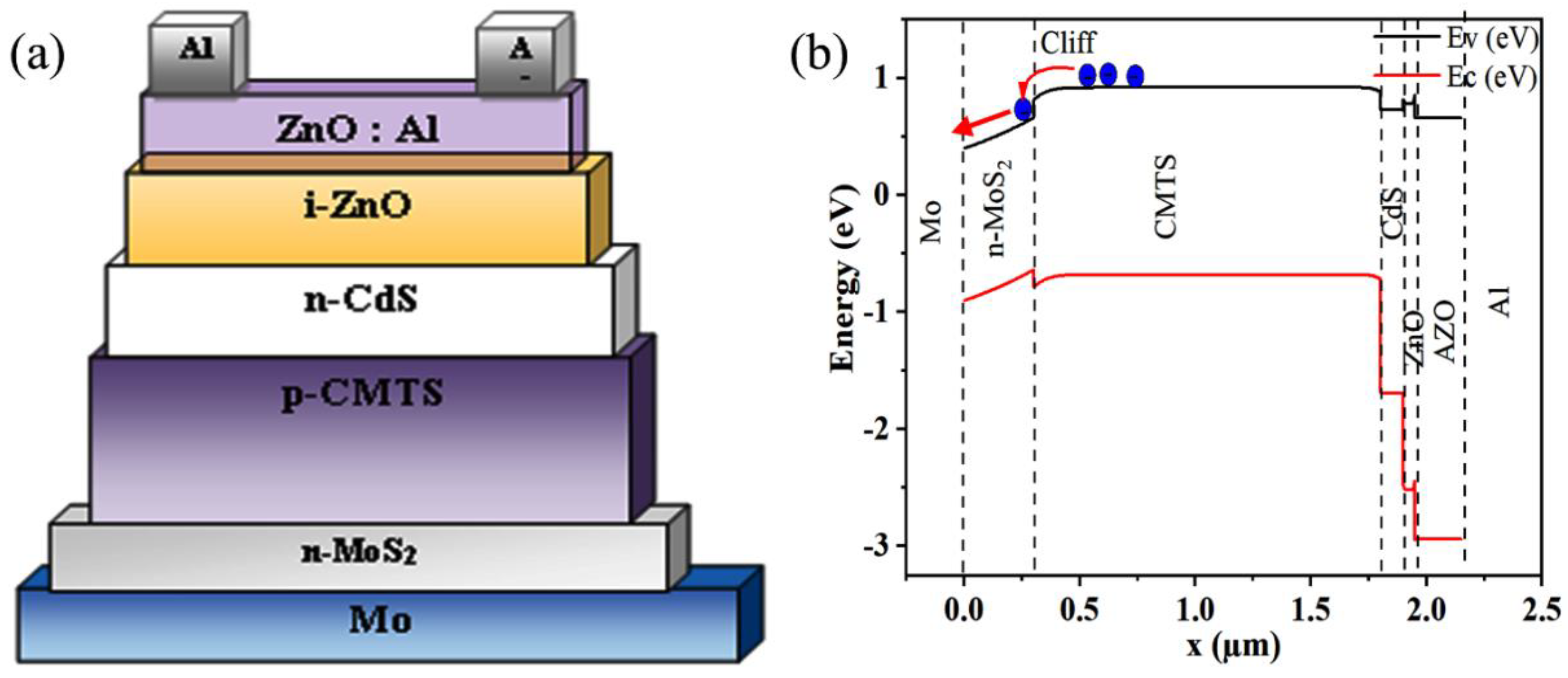
2. Device Structure and Simulation

The device and simulation methodology used are described in this section. A key element in improving the solar cell’s electrical conductivity is the ZnO:Al transparent conduction oxide layer, which enables effective charge carrier movement. On the other hand, the i-ZnO greater resistive layer is crucial in reducing recombination losses within the device, which boosts overall efficiency. A crucial interface between the absorber and front contact, the CdS buffer layer makes it possible to extract photo-generated carriers quickly and effectively. The remarkable light-absorbing qualities of the copper, manganese, tin, and sulfur-based CMTS absorber layer allow it to efficiently capture a variety of solar photons. The Cu2O back surface field (BSF) layer also improves charge collection and lessens rear surface recombination, which eventually improves the performance of the cell. Aluminium (Al) and molybdenum (Mo) are used as the back and front metal contacts, respectively, which helps to achieve the correct band alignment and ensures compatibility with the semiconductor layers. Figure 1 shows a precise schematic illustration of this solar cell construction, giving the reader a visual understanding of its layered structure. The SCAPS-1D simulator, a potent numerical tool specially made for the accurate characterization of thin film solar cell structures, was used for the computational study and modeling of this ground-breaking design. The simulator successfully forecasts the performance characteristics of the device using basic semiconductor equations, such as continuity equations for electrons and holes and Poisson’s equation. The program itself can produce efficiency close to the experimental values if the appropriate defect values are entered. This program simulates the mechanisms of light absorption, the generation of excitons, the transfer of charge and assembly, and recombination. Equation (3) defines Poisson’s equation, which explains how the electrostatic potential and charge density distribution relate to one another [31].
d 2 d x 2 ψ ( x ) = q ε 0 ε r [ p ( x ) n ( x ) + N D N A + ρ p ρ n
where ψ signifies electric potential, ε 0 signifies permittivity of free space, ε r signifies relative permittivity, N D signifies donor density, ρ p signifies hole charge density, N A signifies acceptor density, ρ n signifies electron charge density, and q signifies electronic charge.
Equations (4) and (5) depict the continuity equations for electrons and holes accordingly.
d n d t = 1 q J n x + ( G n R n )
d p d t = 1 q J p x + ( G p R p )
where J n signifies current densities of electrons, G n signifies electron generation rate, J p signifies current densities for holes, G p signifies hole generation rate, R n signifies the recombination rate for electrons, and R p signifies the recombination rate for a hole.
The computation of both the electron current density and the hole current density involves the utilization of the charge carrier drift-diffusion equation, which is given in Equations (6) and (7).
J n = q μ n n + q D n n
J p = q μ p p + q D p p
where D n signifies the electron’s diffusion coefficient, μ n signifies the mobility of electrons, D p signifies the hole’s diffusion coefficient, and μ p signifies the mobility of the hole.
Table 1 lists the precise simulation parameters used in this investigation for comprehensive reference. The solar cell was exposed to illumination from the front contact using the global Air Mass 1.5 spectrum at a dose of 1000 W/m2. The uniformity and comparability of the evaluation of the cell’s effectiveness and performance across diverse research and applications is ensured by the standard testing procedure.

3. Results and Discussion

The schematic device structure is shown in Figure 2a, and the corresponding energy band diagram is shown in Figure 2b. The CMTS solar cell with the structure Mo/n-MoS2/CMTS/CdS/i-ZnO/AZO/Al (Figure 2a) is first simulated and optimized to act as a reference device. The n-MoS2 layer will be examined first to analyze its impact on the cell’s performance. This layer forms spontaneously during the deposition of the CMTS absorber layer on molybdenum. In fact, the sulfur present in the CMTS diffuses towards the molybdenum to create a semiconductor layer of MoS2.
It is observed from the energy band diagram (Figure 2b) that the conduction band offset at the n-MoS2/CMTS interface is negative (cliff-like CBO). This is considered an undesirable band alignment as it facilitates the flow of electrons from CMTS to the rear contact, which is responsible for hole collection, thereby leading to a loss of efficiency of the cell.

3.1. Investigation of the n-MoS2 Layer in the CMTS Solar Cell

MoS2 thin films have been reported to exhibit both n- or p-type conductivity. However, the experimental results reported in the literature mentioned that most of the MoS2 layers formed in CZTS solar cells are n-type due to the presence of native defects of sulfur vacancies. These defects act as deep donors introducing excess electrons into the material, thus leading to n-type behavior [18,52,53,54]. In this simulation study, it was assumed that the MoS2 has n-type conductivity. This phenomenon is important to understand, particularly in the context of thin-film solar cells, because the conductivity type and properties of the MoS2 layers play a critical role in the overall performance of the device.

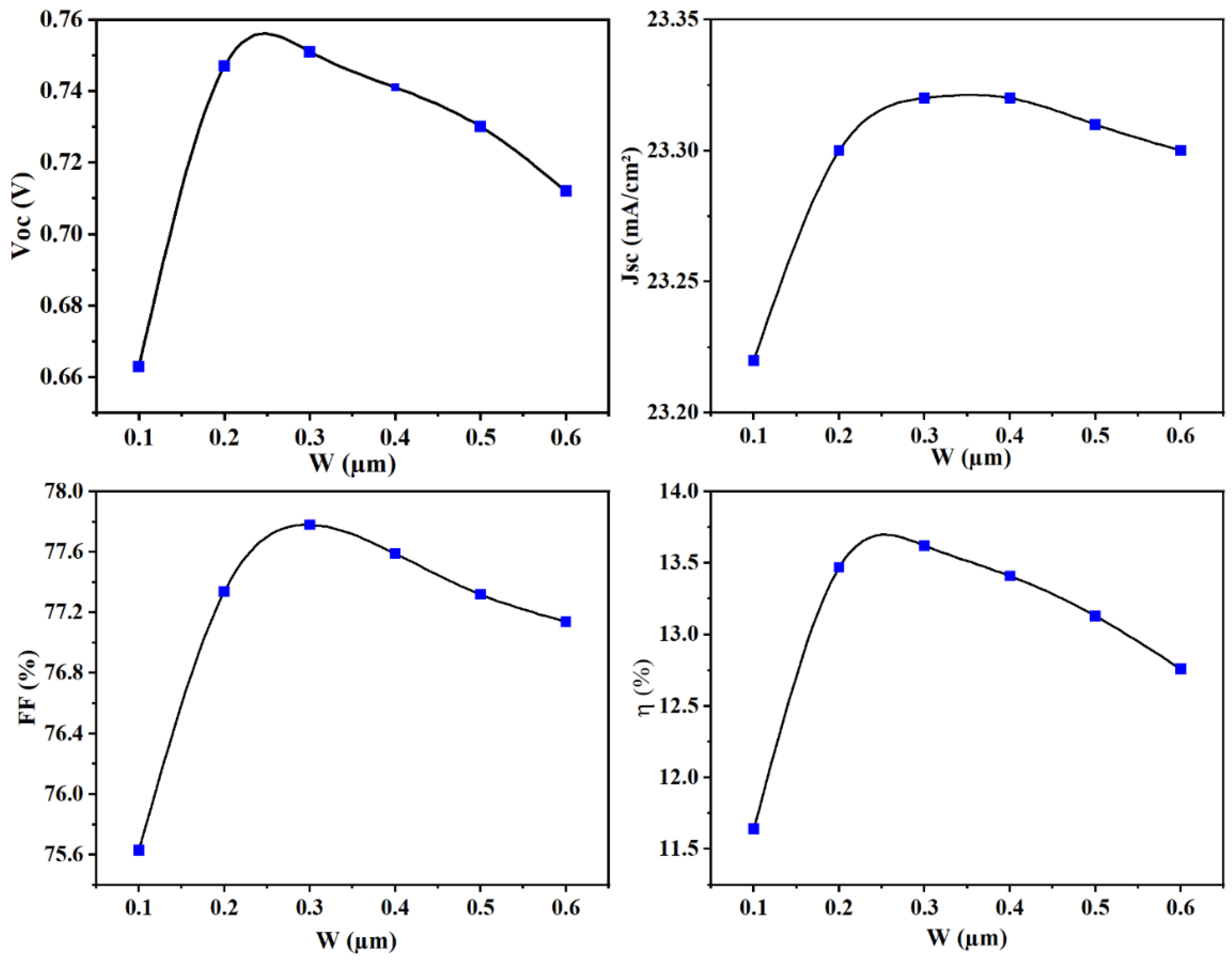
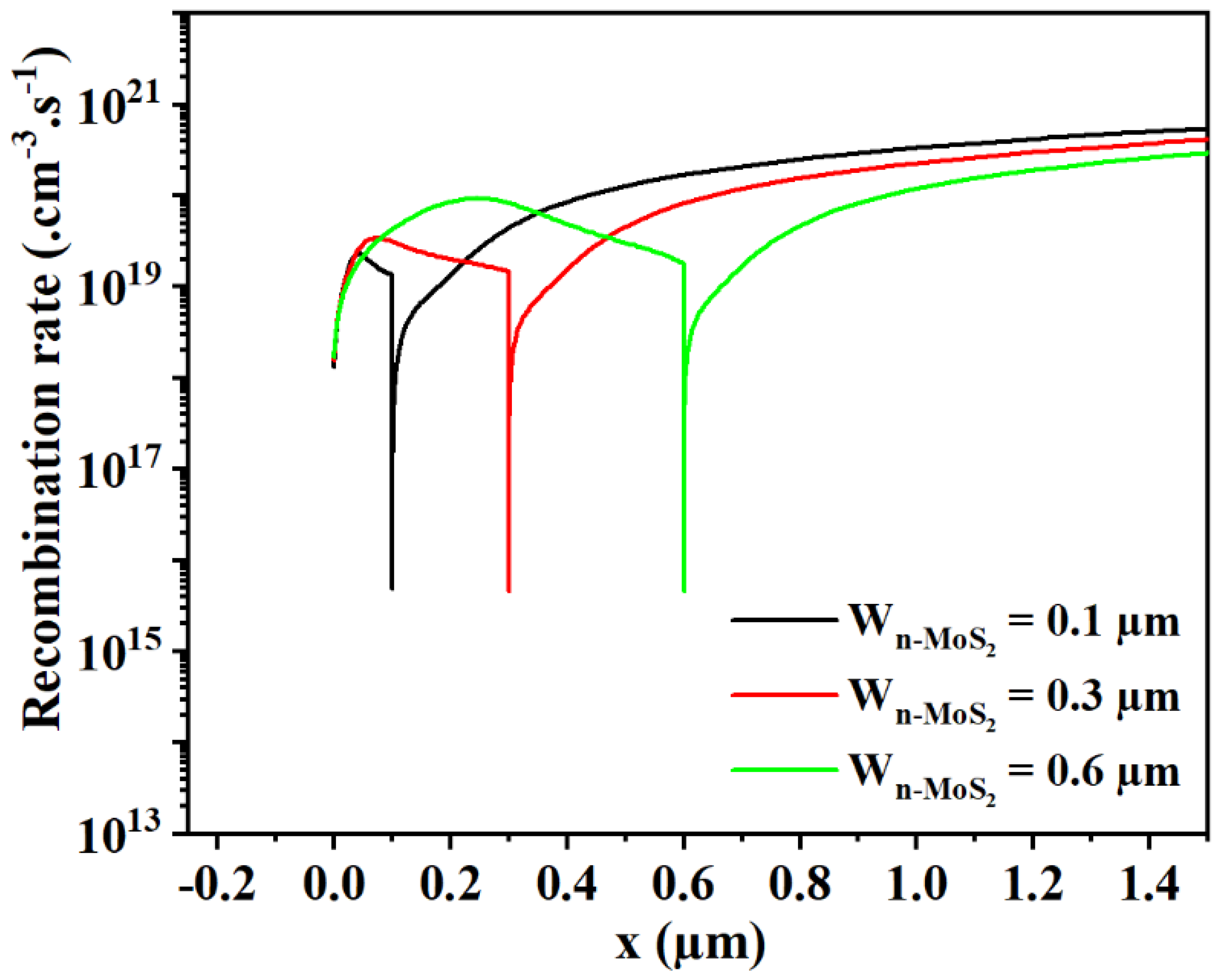
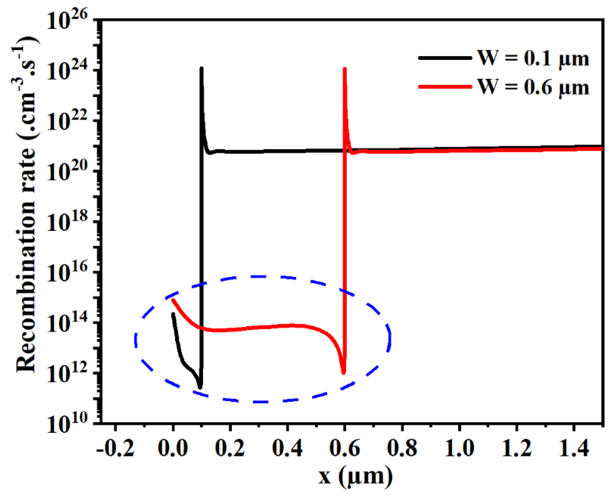
3.1.1. Effect of n-MoS2 Interlayer Thickness on the Performance of the Studied Cell

It is well acknowledged that the thickness of the interfacial MoS2 layer is considered a critical point for device optimization. Thus, the consequence of n-MoS2 interfacial layer thickness on cell PV output was studied in the range of 0.1 to 0.6 µm.
As can be seen in Figure 3, the open circuit voltage (VOC), the fill factor (FF), the short-circuit current (JSC), and the efficiency (η) increase greatly from 0.663 V to 0.751 V, 75.63% to 77.78%, 23.22 mA/cm2 to 23.32 mA/cm2, and 11.64% to 13.62%, correspondingly, when the thickness of n-MoS2 increases from 0.1 to 0.3 µm. However, when the thickness of n-MoS2 is further increased, the recombination rate becomes more important, resulting in the decline of cell outputs (Figure 4). Generally, when the n-MoS2 thickness increases, the photogenerated holes cannot cross easily from p-CMTS to the Mo contact to be collected, and hence the hole current is reduced. Thus, the best outputs of the CMTS-based PV solar cell are obtained while the thickness of n-MoS2 is 0.3 µm.

3.1.2. Effect of n-MoS2 Interlayer Donor Concentration on the Performance of the Studied Cell

To study the impact of the donor density (ND) on the key parameters of the PV solar cell, ND is changed from 1015 to 1019 cm−3, while keeping the n-MoS2 thickness at 0.3 µm as it is the optimal value. As shown in Figure 5, all the key PV parameters like VOC, JSC, FF, and η decrease steadily as ND increases. These parameters decrease from 0.751 V to 0.121 V, 23.32 mA/cm2 to 14.85 mA/cm2, 77.78% to 37.86%, and 13.62% to 0.68%, respectively, in response to higher ND values. Higher ND in MoS2 creates undesirable electric fields at the CMTS/MoS2 interface that restrict the movement of light-generated charge carriers and elevate the carrier recombination by increasing the interface resistance. A similar trend of decrease in PV parameters with an increasing donor concentration of MoS2 is reported in ref. [42].
To justify these results, the recombination rate has been plotted for two different doping concentrations of the n-MoS2 layer (Figure 6). In the heavily doped n-MoS2, large carrier traps are generated, resulting in higher recombination. On another side, the CMTS conduction band energy is higher than that of MoS2, and this forms a cliff-like band alignment in the n-MoS2/p-CMTS interface (Figure 2b), which results in a significantly higher recombination rate. In other words, the easy transfer of electrons from p-CMTS to n-MoS2 increases the electron-hole pair recombination at the n-MoS2 layer. Figure 6 also shows a higher recombination rate in CMST near the n-MoS2/p-CMTS interface, which validates the accumulation of light-generated charge carriers and their recombination within the vicinity of the interface.
The best efficiency η is 13.62% when the n-MoS2 donor concentration is 1015 cm−3 and the thickness is equal to 0.3 µm. Table 2 summarizes the advantageous consequence of utilizing the BSF layer in solar cell technology.

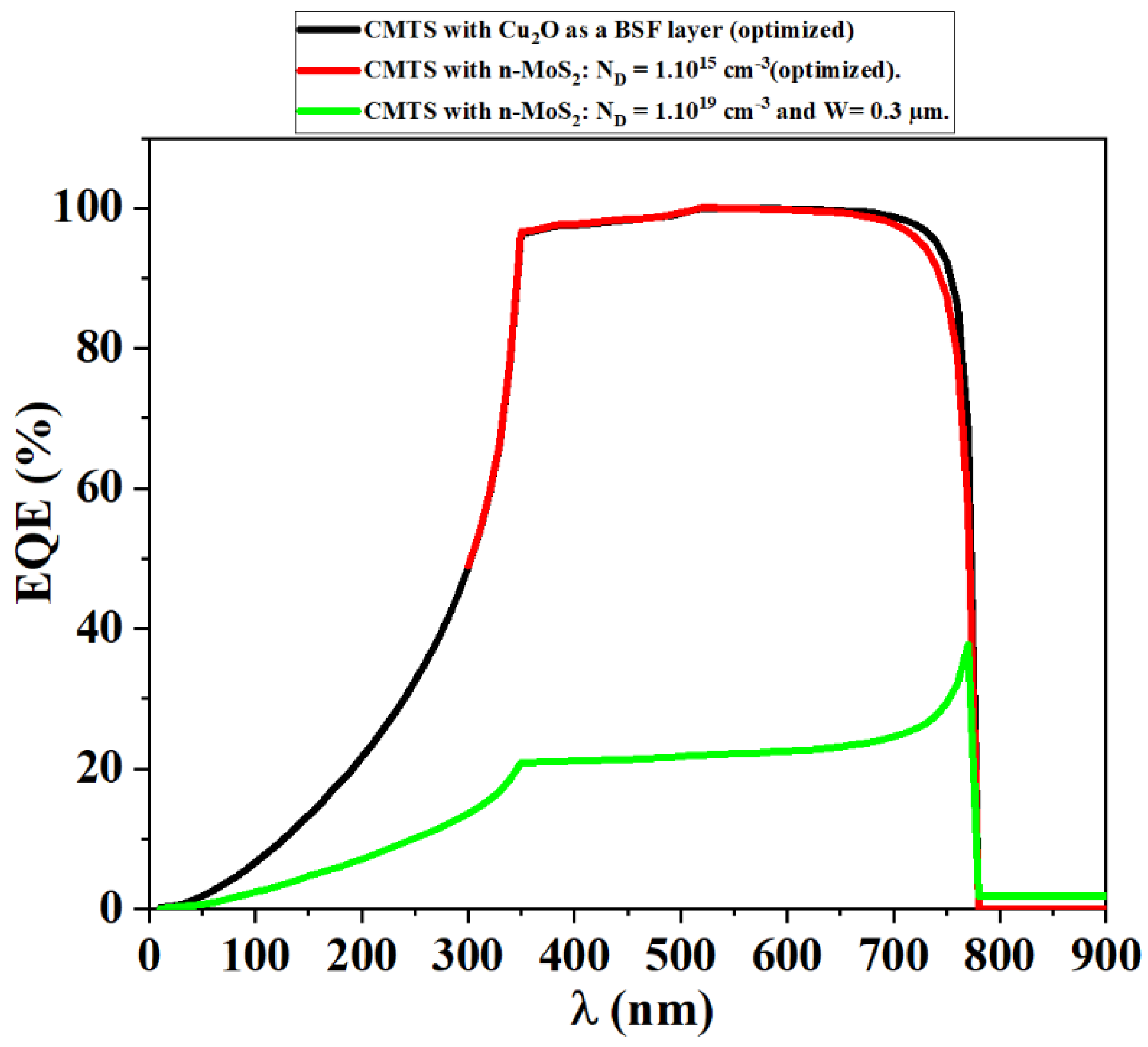
3.2. Impact of the Addition of a Cu2O-Based Back Surface Field (BSF) on the Cell’s Performance

The presence of the BSF layer is crucial in preventing the movement of charge carriers in undesirable directions and preventing interfacial recombination losses. The BSF layer creates an appropriate electric field that acts as an electrical mirror of the charge carrier and pushes the carrier in a backward direction. This phenomenon significantly reduces the recombination rate and elevates the performance of the device. The device under consideration utilizes a Cu2O-based BSF; for better understanding of carrier dynamics within the device, the energy band diagram is obtained and reported in Figure 7.
In order to prevent the spontaneous formation of the n-MoS2 layer, we suggest the incorporation of a Cu2O layer as a back surface field (BSF) on the molybdenum. Figure 7 shows the band alignment of the device by adding Cu2O as a BSF layer to help understand how the incorporation of a Cu2O BSF layer improves PV performance. It is clear from this diagram that by adding the Cu2O layer to the cell structure, the obtained performance is higher due to the large conduction band offset (CBO) spike at the CMTS/Cu2O interface. This spike allows the minority carriers (electrons) at p-CMTS to be backscattered towards the front contact of the cell to be collected, thus preventing them from recombining at the rear face of the device.

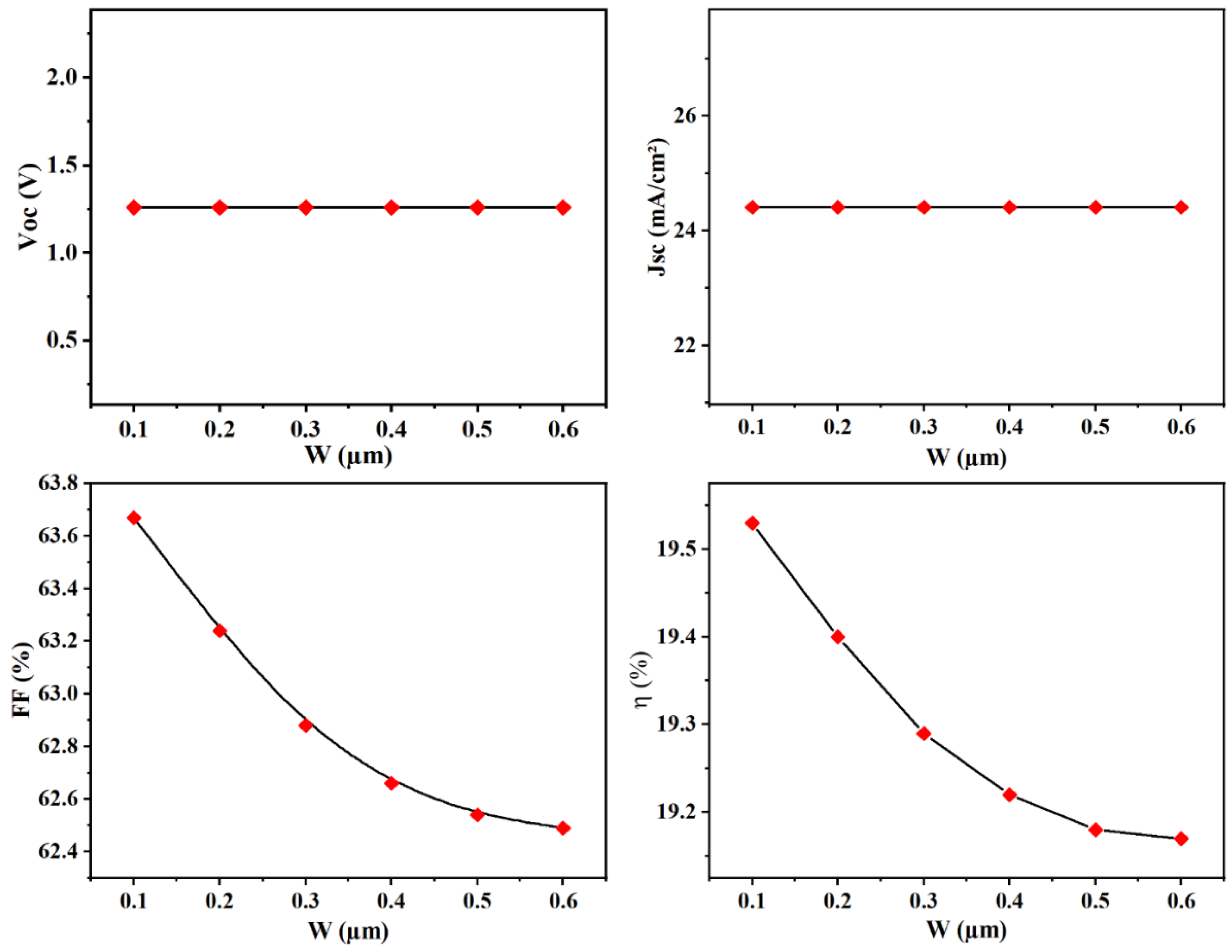
3.2.1. Effect of Cu2O BSF Layer Thickness

It is also important to understand the effect of BSF layer thickness on the performance of the device. Therefore, in this section, the outcome of BSF thickness on cell PV output (VOC, JSC, FF, and η) has been considered in the range of 0.1 to 0.6 µm and presented in Figure 8. It can be noted that both VOC and JSC remain constant at 1.26 V and 24.41 mA/cm2, respectively, while the FF and η decline steadily with increasing the Cu2O BSF layer thickness.
The η goes from 19.53% to 19.17% and shows a clear similarity to the trend seen in the FF (63.67% to 62.49%) curve, so the main factor contributing to the reduction in efficiency is connected with a huge decline in FF. The decline in FF with the increase in Cu2O thickness goes back to the introduction of a resistive component in the PV device. With a thicker BSF, the photogenerated holes must cross distances greater than their diffusion length; hence, it causes a higher recombination rate (Figure 9). In this context, the optimal thickness for the Cu2O BSF was set at 0.1 µm. This specific thickness was chosen after a rigorous evaluation of various thicknesses to achieve the best performance for the solar cell.

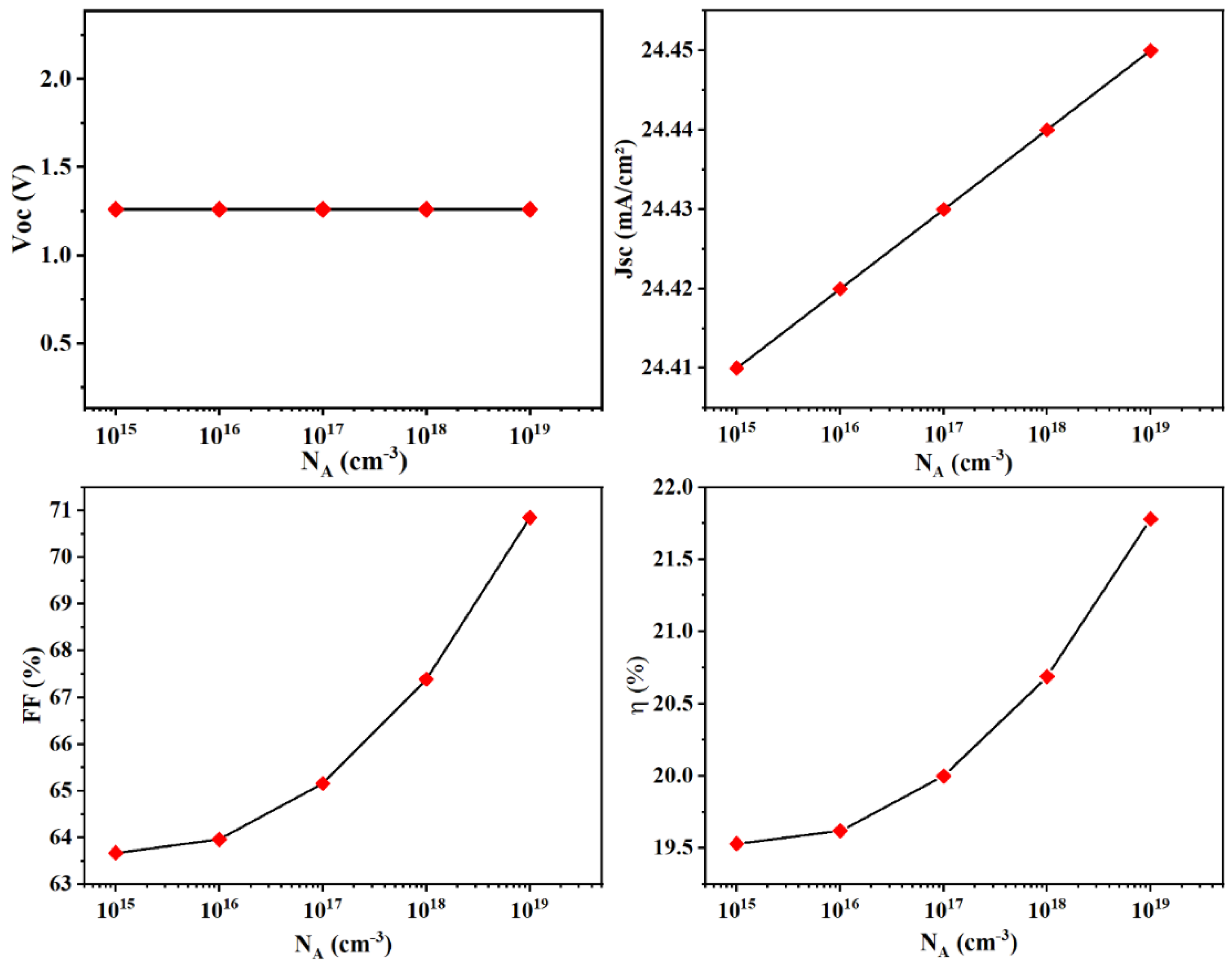
3.2.2. Influence of Cu2O BSF Layer Acceptor Concentration

Acceptor doping in the BSF is one of the crucial parameters that affect the appropriate function of the device as it effectively determines the overall resistive losses in the BSF and the strength of the electric field at the interface. Therefore, in order to analyze the influence of the acceptor concentration density (NA) within the Cu2O back surface field layer, simulations covering a wide range from 1015 to 1019 cm−3 were carried out. The findings from this analysis are visually depicted in Figure 10, showing the correlation between acceptor concentration density and the key performance parameters of the investigated solar cell.
From Figure 10, an increase in Jsc, FF, and η is observed from 24.41 mA/cm2 to 24.45 mA/cm2, 63.67% to 70.85%, and 19.53% to 21.78%, respectively. During the optimization, the VOC remained unchanged, while NA changed from 1015 to 1019 cm−3. A carrier concentration gradient in the Cu2O/CMTS interface produces the built-in potential which blocks the minority carrier flow toward the interface. The observed increase in efficiency can be attributed to the enhancement of the electric field strength at the interface between the Cu2O and CMTS layers as a consequence of increasing the doping concentration in the Cu2O layer. This intensified electric field leads to improved carrier collection efficiency within the solar cell structure. As a result, a higher proportion of generated charge carriers is effectively harvested, contributing to the overall enhancement of the solar cell’s efficiency. This effect underscores the critical role that optimizing the doping concentration of the Cu2O layer plays in augmenting the performance of the photovoltaic device. Finally, after an evaluation of various acceptor concentration densities, the decision was made to optimize the value of NA at 1019 cm−3 This choice was based on the superior photovoltaic (PV) performance characteristics observed at this concentration level, signifying its potential to yield the most favorable outcomes for the solar cell.
External quantum efficiency (EQE) is defined as the ratio of the number of carriers generated in the solar cell by an incident photon at a given wavelength. The optical performance of the device is probed using EQE. Three devices, namely CMTS with n-MoS2 (1 × 1019 cm−3), CMTS with n-MoS2 (1 × 1015 cm−3), and CMTS with Cu2O (BSF), are subjected to optical study by simulating the EQE data in the wavelength range until 900 nm. Figure 11 shows the comparison of the external quantum efficiency (EQE) curves for Al/AZO/ZnO/CdS/CMTS/n-MoS2/Mo and Al/AZO/ZnO/CdS/CMTS/Cu2O/Mo structures in the wavelength range from 10 nm to 900 nm.
By incorporating the Cu2O as a BSF layer, good performance has been revealed due to the Cu2O’s properties, which makes it a good candidate for photovoltaic applications [59,60,61,62]. A similar increase in performance parameters (JSC, FF, η) with increasing the doping concentration of the BSF layer is reported in refs. [63,64].
From this analysis, it has been found that after adding Cu2O as a BSF layer, the efficiency of CMTS-based solar cells increases up to 21.78%. A comparison of experimental and theoretical values (provided from the literature) is given in Table 3. The results are found to be in good accord with the previous simulation outputs. It is clear from the data in this table that many challenges remain in the experimental development of CMTS solar cells. One of the main reasons for the observed lower experimental outputs of CMTS-based solar cells without a BSF layer is the formation of uncontrollable n-MoS2 films, which have unfavorable effects on cell performance.
While our study provides valuable insights into the potential benefits of incorporating Cu2O in CMTS solar cells, it is essential to acknowledge that our proposal involving Cu2O as a BSF layer requires experimental validation to assess its feasibility.

4. Conclusions

This paper addresses a critical limitation in the development of CMTS solar cells, which is the formation of a MoS2 intermediate layer. To illustrate the impact of variations in MoS2 parameters, a numerical simulation of a reference device with the structure Mo/n-MoS2/CMTS/CdS/i-ZnO/AZO/Al was performed. Given the uncontrollable parameters of MoS2, our goal was not to achieve higher performance but to demonstrate how even slight variations in MoS2 parameters can significantly affect the device’s performance. In order to avoid the adverse effect of the MoS2 layer, the addition of Cu2O as a BSF layer between the molybdenum and the CMTS absorber was proposed and studied. The optimal physical properties of this layer (thickness and acceptor concentration) have been identified. According to the optimization, the highest efficiency achieved with a Cu2O BSF layer is 21.78% for a thickness of 0.1 µm and a doping density of 1019 cm−3, which is much higher than the results obtained previously in the literature. Furthermore, the presence of Cu2O as a BSF layer provides a desirable spike-like CBO which prevents the easy transfer and the recombination of electrons from the absorber layer to the back contact. In conclusion, the results presented in this study offer significant and enlightening insights that hold great promise for advancing the development of photovoltaic (PV) solar cells based on CMTS materials, with the potential to substantially enhance their efficiency and overall performance. These findings underscore the importance of further research and optimization efforts in harnessing the full potential of CMTS-based PV technology, thus contributing to the ongoing evolution of sustainable and efficient energy generation.

Author Contributions

Conceptualization, W.L.R., L.B.F. and R.P.; Methodology, W.H., W.L.R., G.F.I.T., M.K.A.M., S.E., R.P. and M.K.H.; Software, W.H., G.F.I.T., M.K.A.M., L.B.F., S.E., A.B. and M.K.H.; Validation, W.L.R., M.K.A.M., L.B.F., R.P., A.B. and M.K.H.; Formal analysis, W.H., W.L.R., M.K.A.M., L.B.F., A.B. and M.K.H.; Investigation, W.H., W.L.R., S.E., A.B. and M.K.H.; Data curation, A.B.; Writing—original draft, W.H., W.L.R., G.F.I.T. and M.K.H.; Writing—review & editing, W.L.R., G.F.I.T., M.K.A.M., L.B.F., S.E., A.B. and M.K.H.; Visualization, A.B.; Funding acquisition, R.P. All authors have read and agreed to the published version of the manuscript.

Funding

This research was funded by King Khalid University, Saudi Arabia, grant number [R.G.P.2: 233/44].

Institutional Review Board Statement

Not applicable.

Informed Consent Statement

Not applicable.

Data Availability Statement

Not applicable.

Acknowledgments

The authors have extended their appreciation to the Deanship of Scientific Research at King Khalid University, Saudi Arabia for funding this work through the Research Groups Program under grant number R.G.P.2: 233/44. The SCAPS-1D program was kindly provided by M. Burgelman of the University of Gent in Belgium. The authors would like to express their gratitude to him.

Conflicts of Interest

The authors declare no conflict of interest.

References

  1. Dureja, T.; Garg, A.; Bhalla, S.; Bhutani, D.; Khanna, A. Double Lead-Free Perovskite Solar Cell for 19.9% Conversion Efficiency: A SCAPS-1D Based Simulation Study. Mater. Today Proc. 2022, 71, 239–242. [Google Scholar] [CrossRef]
  2. Pandey, R.; Khanna, A.; Singh, K.; Patel, S.K.; Singh, H.; Madan, J. Device Simulations: Toward the Design of >13% Efficient PbS Colloidal Quantum Dot Solar Cell. Sol. Energy 2020, 207, 893–902. [Google Scholar] [CrossRef]
  3. Thakur, A.; Singh, D.; Kaur Gill, S. Numerical Simulations of 26.11% Efficient Planar CH3NH3PbI3 Perovskite n-i-p Solar Cell. Mater. Today Proc. 2022, 71, 195–201. [Google Scholar] [CrossRef]
  4. Kumar, R.; Kumar, A.; Pushkar, R.; Priyadarshi, A. The Impact of SnMnO2 TCO and Cu2O as a Hole Transport Layer on CIGSSe Solar Cell Performance Improvement. J. Comput. Electron. 2023, 22, 1107–1127. [Google Scholar] [CrossRef]
  5. Isha, A.; Kowsar, A.; Kuddus, A.; Hossain, M.K.; Ali, M.H.; Haque, M.D.; Rahman, M.F. High Efficiency Cu2MnSnS4 Thin Film Solar Cells with SnS BSF and CdS ETL Layers: A Numerical Simulation. Heliyon 2023, 9, e15716. [Google Scholar] [CrossRef]
  6. Chinnasamy, V.; Palaniappan, S.K.; Raj, M.K.A.; Rajendran, M.; Cho, H. Thermal Energy Storage and Its Applications. In Materials for Solar Energy Conversion; Wiley: Hoboken, NJ, USA, 2021; pp. 353–377. [Google Scholar]
  7. Shin, M.J.; Lee, A.; Cho, A.; Kim, K.; Ahn, S.K.; Park, J.H.; Yoo, J.; Yun, J.H.; Gwak, J.; Shin, D.; et al. Semitransparent and Bifacial Ultrathin Cu(In,Ga)Se2 Solar Cells via a Single-Stage Process and Light-Management Strategy. Nano Energy 2021, 82, 105729. [Google Scholar] [CrossRef]
  8. El Radaf, I.M. Intensive Studies on the Structural, Optical, and Optoelectrical Properties of a Novel Kesterite Cu2CdGeS4 Thin Films. Optik 2023, 272, 170358. [Google Scholar] [CrossRef]
  9. Katagiri, H.; Jimbo, K.; Maw, W.S.; Oishi, K.; Yamazaki, M.; Araki, H.; Takeuchi, A. Development of CZTS-Based Thin Film Solar Cells. Thin Solid Films 2009, 517, 2455–2460. [Google Scholar] [CrossRef]
  10. Green, M.A.; Dunlop, E.D.; Siefer, G.; Yoshita, M.; Kopidakis, N.; Bothe, K.; Hao, X. Solar Cell Efficiency Tables (Version 61). Prog. Photovoltaics Res. Appl. 2023, 31, 3–16. [Google Scholar] [CrossRef]
  11. Shockley, W.; Queisser, H.J. Detailed Balance Limit of Efficiency of P-n Junction Solar Cells. J. Appl. Phys. 1961, 32, 510–519. [Google Scholar] [CrossRef]
  12. Sun, S.; Guo, J.; Hao, R.; Aierken, A.; Liu, B.; Gu, K.; Wang, L.; Ma, X.; Wei, G.; Cai, J.; et al. Influence of Cd0.6Zn0.4S Buffer Layer on the Band Alignment and the Performance of CZTS Thin Film Solar Cells. Opt. Mater. 2021, 112, 110666. [Google Scholar] [CrossRef]
  13. Kumar, M.S.; Madhusudanan, S.P.; Batabyal, S.K. Substitution of Zn in Earth-Abundant Cu2ZnSn(S,Se)4 Based Thin Film Solar Cells—A Status Review. Sol. Energy Mater. Sol. Cells 2018, 185, 287–299. [Google Scholar] [CrossRef]
  14. Prabhakar, R.R.; Zhenghua, S.; Xin, Z.; Baikie, T.; Woei, L.S.; Shukla, S.; Batabyal, S.K.; Gunawan, O.; Wong, L.H. Photovoltaic Effect in Earth Abundant Solution Processed Cu2MnSnS4 and Cu2MnSn(S,Se)4 Thin Films. Sol. Energy Mater. Sol. Cells 2016, 157, 867–873. [Google Scholar] [CrossRef]
  15. Le Donne, A.; Marchionna, S.; Acciarri, M.; Cernuschi, F.; Binetti, S. Relevant Efficiency Enhancement of Emerging Cu2MnSnS4 Thin Film Solar Cells by Low Temperature Annealing. Sol. Energy 2017, 149, 125–131. [Google Scholar] [CrossRef]
  16. Johnson, J.; Nukala, H.; Lund, E.; Hlaing Oo, W.M.; Bhatia, A.; Rieth, L.W.; Scarpulla, M.A. Effects of 2nd Phases, Stress, and Na at the Mo/Cu2ZnSnS4 Interface. MRS Online Proc. Libr. 2010, 1268, 3–8. [Google Scholar] [CrossRef]
  17. Kumari, N.; Ingole, S. Enhancement of CZTS Photovoltaic Device Performance with Silicon at Back-Contact: A Study Using SCAPS-1D. Sol. Energy 2022, 236, 301–307. [Google Scholar] [CrossRef]
  18. Ferdaous, M.T.; Shahahmadi, S.A.; Chelvanathan, P.; Akhtaruzzaman, M.; Alharbi, F.H.; Sopian, K.; Tiong, S.K.; Amin, N. Elucidating the Role of Interfacial MoS2 Layer in Cu2ZnSnS4 Thin Film Solar Cells by Numerical Analysis. Sol. Energy 2019, 178, 162–172. [Google Scholar] [CrossRef]
  19. Karade, V.; Lokhande, A.; Babar, P.; Gang, M.G.; Suryawanshi, M.; Patil, P.; Kim, J.H. Insights into Kesterite’s Back Contact Interface: A Status Review. Sol. Energy Mater. Sol. Cells 2019, 200, 109911. [Google Scholar] [CrossRef]
  20. Li, W.; Chen, J.; Cui, H.; Liu, F.; Hao, X. Inhibiting MoS2 Formation by Introducing a ZnO Intermediate Layer for Cu2ZnSnS4 Solar Cells. Mater. Lett. 2014, 130, 87–90. [Google Scholar] [CrossRef]
  21. Rana, M.S.; Islam, M.M.; Julkarnain, M. Enhancement in Efficiency of CZTS Solar Cell by Using CZTSe BSF Layer. Sol. Energy 2021, 226, 272–287. [Google Scholar] [CrossRef]
  22. Ghobadi, A.; Yousefi, M.; Minbashi, M.; Kordbacheh, A.H.A.; Abdolvahab, A.H.; Gorji, N.E. Simulating the Effect of Adding BSF Layers on Cu2BaSnSSe3 Thin Film Solar Cells. Opt. Mater. 2020, 107, 109927. [Google Scholar] [CrossRef]
  23. Tran, M.H.; Cho, J.Y.; Sinha, S.; Gang, M.G.; Heo, J. Cu2O/ZnO Heterojunction Thin-Film Solar Cells: The Effect of Electrodeposition Condition and Thickness of Cu2O. Thin Solid Films 2018, 661, 132–136. [Google Scholar] [CrossRef]
  24. Lakshmanan, A.; Alex, Z.C.; Meher, S.R. Cu2O Thin Films Grown by Magnetron Sputtering as Solar Cell Absorber Layers. Mater. Sci. Semicond. Process. 2022, 148, 106818. [Google Scholar] [CrossRef]
  25. Wisz, G.; Sawicka-Chudy, P.; Yavorskyi, R.; Potera, P.; Bester, M.; Głowa, Ł. TiO2/Cu2O Heterojunctions for Photovoltaic Cells Application Produced by Reactive Magnetron Sputtering. Mater. Today Proc. 2021, 35, 552–557. [Google Scholar] [CrossRef]
  26. Ugalde-Reygadas, M.; Moreno-Regino, V.D.; Torres-Castanedo, C.G.; Bedzyk, M.J.; Castanedo-Pérez, R.; Torres-Delgado, G. Cu2O Thin Films Deposited by Spray Pyrolysis Using Diethanolamine and L-Ascorbic Acid as Reducing Agents. Mater. Today Commun. 2022, 32, 103999. [Google Scholar] [CrossRef]
  27. Pansuriya, T.; Malani, R.; Kheraj, V. Investigations on the Effect of Buffer Layer on CMTS Based Thin Film Solar Cell Using SCAPS 1-D. Opt. Mater. 2022, 126, 112150. [Google Scholar] [CrossRef]
  28. Khattak, Y.H.; Baig, F.; Marí, B.; Beg, S.; Ahmed, S. Baseline for the Numerical Analysis of High Efficiency Copper Manganese Tin Sulfide Cu2MnSnS4 Based Thin Film Solar Cell. J. Nanoelectron. Optoelectron. 2018, 13, 1678–1684. [Google Scholar] [CrossRef]
  29. Hossain, M.K.; Arnab, A.A.; Samajdar, D.P.; Rubel, M.H.K.; Hossain, M.M.; Islam, M.R.; Das, R.C.; Bencherif, H.; Rahman, M.F.; Madan, J.; et al. Design Insights into La2NiMnO6-Based Perovskite Solar Cells Employing Different Charge Transport Layers: DFT and SCAPS-1D Frameworks. Energy Fuels 2023, 37, 13377–13396. [Google Scholar] [CrossRef]
  30. Hossain, M.K.; Toki, G.F.I.; Kuddus, A.; Mohammed, M.K.A.; Pandey, R.; Madan, J.; Bhattarai, S.; Rahman, M.F.; Dwivedi, D.K.; Amami, M.; et al. Optimization of the Architecture of Lead-Free CsSnCl3-Perovskite Solar Cells for Enhancement of Efficiency: A Combination of SCAPS-1D and WxAMPS Study. Mater. Chem. Phys. 2023, 308, 128281. [Google Scholar] [CrossRef]
  31. Jabr, R.A.; Hamad, M.; Mohanna, Y.M. Newton-Raphson Solution of Poisson’s Equation in a Pn Diode. Int. J. Electr. Eng. Educ. 2007, 44, 23–33. [Google Scholar] [CrossRef]
  32. Biplab, S.R.I.; Ali, M.H.; Moon, M.M.A.; Pervez, M.F.; Rahman, M.F.; Hossain, J. Performance Enhancement of CIGS-Based Solar Cells by Incorporating an Ultrathin BaSi2 BSF Layer. J. Comput. Electron. 2020, 19, 342–352. [Google Scholar] [CrossRef]
  33. Bibi, B.; Farhadi, B.; ur Rahman, W.; Liu, A. A Novel Design of CTZS/Si Tandem Solar Cell: A Numerical Approach. J. Comput. Electron. 2021, 20, 1769–1778. [Google Scholar] [CrossRef]
  34. Scarpulla, M.A.; McCandless, B.; Phillips, A.B.; Yan, Y.; Heben, M.J.; Wolden, C.; Xiong, G.; Metzger, W.K.; Mao, D.; Krasikov, D.; et al. CdTe-Based Thin Film Photovoltaics: Recent Advances, Current Challenges and Future Prospects. Sol. Energy Mater. Sol. Cells 2023, 255, 112289. [Google Scholar] [CrossRef]
  35. Bouarissa, A.; Gueddim, A.; Bouarissa, N.; Maghraoui-Meherezi, H. Modeling of ZnO/MoS2/CZTS Photovoltaic Solar Cell through Window, Buffer and Absorber Layers Optimization. Mater. Sci. Eng. B 2021, 263, 114816. [Google Scholar] [CrossRef]
  36. Hossain, M.K.; Arnab, A.A.; Das, R.C.; Hossain, K.M.; Rubel, M.H.K.; Rahman, M.F.; Bencherif, H.; Emetere, M.E.; Mohammed, M.K.A.; Pandey, R. Combined DFT, SCAPS-1D, and WxAMPS Frameworks for Design Optimization of Efficient Cs2BiAgI6-Based Perovskite Solar Cells with Different Charge Transport Layers. RSC Adv. 2022, 12, 34850–34873. [Google Scholar] [CrossRef]
  37. Hossain, M.K.; Rubel, M.H.K.; Toki, G.F.I.; Alam, I.; Rahman, M.F.; Bencherif, H. Effect of Various Electron and Hole Transport Layers on the Performance of CsPbI3-Based Perovskite Solar Cells: A Numerical Investigation in DFT, SCAPS-1D, and WxAMPS Frameworks. ACS Omega 2022, 7, 43210–43230. [Google Scholar] [CrossRef]
  38. Raoui, Y.; Ez-Zahraouy, H.; Tahiri, N.; El Bounagui, O.; Ahmad, S.; Kazim, S. Performance Analysis of MAPbI3 Based Perovskite Solar Cells Employing Diverse Charge Selective Contacts: Simulation Study. Sol. Energy 2019, 193, 948–955. [Google Scholar] [CrossRef]
  39. Sajid, S.; Alzahmi, S.; Salem, I.B.; Obaidat, I.M. Guidelines for Fabricating Highly Efficient Perovskite Solar Cells with Cu2O as the Hole Transport Material. Nanomaterials 2022, 12, 3315. [Google Scholar] [CrossRef] [PubMed]
  40. Chen, L.; Deng, H.; Tao, J.; Zhou, W.; Sun, L.; Yue, F.; Yang, P.; Chu, J. Influence of Annealing Temperature on Structural and Optical Properties of Cu2MnSnS4 Thin Films Fabricated by Sol–Gel Technique. J. Alloys Compd. 2015, 640, 23–28. [Google Scholar] [CrossRef]
  41. Güneri, E.; Aker, D.; Henry, J.; Billur, C.A.; Saatçi, B. Cu2O Thin Films Prepared by Chemical Bath Deposition: An Improved Method. Phase Transit. 2022, 95, 679–690. [Google Scholar] [CrossRef]
  42. Luo, H.; Zhang, Y.; Li, H. Effect of MoS2 Interlayer on Performances of Copper-Barium-Tin-Sulfur Thin Film Solar Cells via Theoretical Simulation. Sol. Energy 2021, 223, 384–397. [Google Scholar] [CrossRef]
  43. Wang, Y.; Kai Gary Kwok, C.; Xiao, D.; Zhu, J.; Shu, X.; Ping Liu, C.; Man Yu, K. Improving the p–Type Conductivity of Cu2O Thin Films by Ni Doping and Their Heterojunction with n–ZnO. Appl. Surf. Sci. 2022, 590, 153047. [Google Scholar] [CrossRef]
  44. Derbal, S.; Benaicha, M. Insights on the Effect of Applied Potential on the Properties of Electrodeposited P-Type Cuprous Oxide (Cu2O) Thin Films. J. Electron. Mater. 2021, 50, 5134–5140. [Google Scholar] [CrossRef]
  45. Khattak, Y.H.; Baig, F.; Toura, H.; Beg, S.; Soucase, B.M. Efficiency Enhancement of Cu2BaSnS4 Experimental Thin-Film Solar Cell by Device Modeling. J. Mater. Sci. 2019, 54, 14787–14796. [Google Scholar] [CrossRef]
  46. Gupta, G.K.; Dixit, A. Simulation Studies on Photovoltaic Response of Ultrathin CuSb(S/Se)2 Ternary Compound Semiconductors Absorber-Based Single Junction Solar Cells. Int. J. Energy Res. 2020, 44, 3724–3736. [Google Scholar] [CrossRef]
  47. Lin, J.; Xu, J.; Yang, Y. Numerical Analysis of the Effect of MoS2 Interface Layers on Copper-Zinc-Tin-Sulfur Thin Film Solar Cells. Optik 2020, 201, 163496. [Google Scholar] [CrossRef]
  48. Sharbati, S.; Gharibshahian, I.; Orouji, A.A. Designing of AlxGa1-XAs/CIGS Tandem Solar Cell by Analytical Model. Sol. Energy 2019, 188, 1–9. [Google Scholar] [CrossRef]
  49. Basak, A.; Singh, U.P. Numerical Modelling and Analysis of Earth Abundant Sb2S3 and Sb2Se3 Based Solar Cells Using SCAPS-1D. Sol. Energy Mater. Sol. Cells 2021, 230, 111184. [Google Scholar] [CrossRef]
  50. El Otmani, R.; El Manouni, A.; Al Maggoussi, A. Numerical Simulation of CZTSe Based Solar Cells Using Different Back Surface Field Layers: Improvement and Comparison. J. Electron. Mater. 2021, 50, 2021–2033. [Google Scholar] [CrossRef]
  51. Beyrami, N.; Saadat, M.; Sohbatzadeh, Z. A Modeling Study on Utilizing In2S3 as a Buffer Layer in CIGS-Based Solar Cells. J. Comput. Electron. 2022, 21, 1329–1337. [Google Scholar] [CrossRef]
  52. Akdim, B.; Pachter, R.; Mou, S. Theoretical Analysis of the Combined Effects of Sulfur Vacancies and Analyte Adsorption on the Electronic Properties of Single-Layer MoS2. Nanotechnology 2016, 27, 185701. [Google Scholar] [CrossRef] [PubMed]
  53. Yang, K.-J.; Sim, J.-H.; Jeon, B.; Son, D.-H.; Kim, D.-H.; Sung, S.-J.; Hwang, D.-K.; Song, S.; Khadka, D.B.; Kim, J.; et al. Effects of Na and MoS2 on Cu2ZnSnS4 Thin-Film Solar Cell. Prog. Photovoltaics Res. Appl. 2015, 23, 862–873. [Google Scholar] [CrossRef]
  54. Wei, Z.; Fung, C.M.; Pockett, A.; Dunlop, T.O.; McGettrick, J.D.; Heard, P.J.; Guy, O.J.; Carnie, M.J.; Sullivan, J.H.; Watson, T.M. Engineering of a Mo/SixNy Diffusion Barrier to Reduce the Formation of MoS2 in Cu2ZnSnS4 Thin Film Solar Cells. ACS Appl. Energy Mater. 2018, 1, 2749–2757. [Google Scholar] [CrossRef]
  55. Kaminski, A.; Vandelle, B.; Fave, A.; Boyeaux, J.; Nam, L.Q.; Monna, R.; Sarti, D.; Laugier, A. Aluminium BSF in Silicon Solar Cells. Sol. Energy Mater. Sol. Cells 2002, 72, 373–379. [Google Scholar] [CrossRef]
  56. Yang, X.; Chen, B.; Chen, J.; Zhang, Y.; Liu, W.; Sun, Y. ZnS Thin Film Functionalized as Back Surface Field in Si Solar Cells. Mater. Sci. Semicond. Process. 2018, 74, 309–312. [Google Scholar] [CrossRef]
  57. Kohara, N.; Nishiwaki, S.; Hashimoto, Y.; Negami, T.; Wada, T. Electrical Properties of the Cu(In,Ga)Se2/ MoSe2/Mo Structure. Sol. Energy Mater. Sol. Cells 2001, 67, 209–215. [Google Scholar] [CrossRef]
  58. Shukla, V.; Panda, G. Effect of BSF Layer on the Performance of CdTe Solar Cell. Mater. Today Proc. 2021, 44, 2300–2303. [Google Scholar] [CrossRef]
  59. Camacho-Espinosa, E.; Rimmaudo, I.; Riech, I.; Mis-Fernández, R.; Peña, J.L. Stability of Sputter Deposited Cuprous Oxide (Cu2O) Subjected to Ageing Conditions for Photovoltaic Applications. J. Appl. Phys. 2018, 123, 8. [Google Scholar] [CrossRef]
  60. Abdelfatah, M.; Ledig, J.; El-Shaer, A.; Wagner, A.; Marin-Borras, V.; Sharafeev, A.; Lemmens, P.; Mosaad, M.M.; Waag, A.; Bakin, A. Fabrication and Characterization of Low Cost Cu2O/ZnO:Al Solar Cells for Sustainable Photovoltaics with Earth Abundant Materials. Sol. Energy Mater. Sol. Cells 2016, 145, 454–461. [Google Scholar] [CrossRef]
  61. Kumar, R.; Bergum, K.; Riise, H.N.; Monakhov, E.; Galeckas, A.; Svensson, B.G. Impact of Post Annealing and Hydrogen Implantation on Functional Properties of Cu2O Thin Films for Photovoltaic Applications. J. Alloys Compd. 2020, 825, 153982. [Google Scholar] [CrossRef]
  62. Salah, H.Y.; Abdelfatah, M.; El-Shaer, A.; Oraby, A.H. Effect of Al Doped ZnO on Optical and Photovoltaic Properties of the P-Cu2O/n-AZO Solar Cells. Ceram. Int. 2022, 49, 7746–7752. [Google Scholar] [CrossRef]
  63. Bag, A.; Radhakrishnan, R.; Nekovei, R.; Jeyakumar, R. Effect of Absorber Layer, Hole Transport Layer Thicknesses, and Its Doping Density on the Performance of Perovskite Solar Cells by Device Simulation. Sol. Energy 2020, 196, 177–182. [Google Scholar] [CrossRef]
  64. Atowar Rahman, M. Enhancing the Photovoltaic Performance of Cd-Free Cu2ZnSnS4 Heterojunction Solar Cells Using SnS HTL and TiO2 ETL. Sol. Energy 2021, 215, 64–76. [Google Scholar] [CrossRef]
  65. Wang, W.; Chen, B.; Chen, G.; Cai, H.; Dong, J.; Liao, Y.; Chen, S.; Huang, Z. A General Oxide-Based Preparation Strategy for Cu2MSnS4 (M: Zn, Mn, Cd) Thin Films and Relevant Solar Cells. Mater. Lett. 2018, 214, 170–173. [Google Scholar] [CrossRef]
Figure 1. Schematic illustration of the proposed CMTS construction.
Sustainability 15 14322 g001
Figure 2. (a) Schematic and (b) energy band diagrams of the Mo/n-MoS2/CMTS/CdS/i-ZnO/AZO/Al heterojunction solar cell.
Sustainability 15 14322 g002
Figure 3. Effect of n-MoS2 thickness on cell performance.
Sustainability 15 14322 g003
Figure 4. Effect of n-MoS2 thickness on recombination rate.
Sustainability 15 14322 g004
Figure 5. Effect of n-MoS2 doping density on cell performance.
Sustainability 15 14322 g005
Figure 6. Influence of donor concentration on recombination rate.
Sustainability 15 14322 g006
Figure 7. Energy band alignment of the projected solar cell with Cu2O as a BSF layer.
Sustainability 15 14322 g007
Figure 8. Effect of Cu2O thickness on the photovoltaic parameters.
Sustainability 15 14322 g008
Figure 9. Influence of thickness of the Cu2O BSF on recombination rate.
Sustainability 15 14322 g009
Figure 10. Effect of Cu2O acceptor concentration on the photovoltaic parameters.
Sustainability 15 14322 g010
Figure 11. External quantum efficiency spectra vs. wavelength of CMTS solar cells with and without the Cu2O BSF layer.
Sustainability 15 14322 g011
Table 1. Features set for simulation of CMTS-based solar cells [22,28,32,33,34,35,36,37,38,39,40,41,42,43,44,45,46,47,48,49,50,51].
Featuresp-Cu2On-MoS2p-CMTSn-CdSi-ZnOn-AZO
Thickness (µm)0.1–0.60.1–0.61.50.10.050.2
Eg (eV)2.21.31.62.423.33.6
εr7.113.698.2599
X (eV)3.24.54.354.54.44.6
NC (cm−3)2.5 × 10187.5 × 10172.2 × 10183.1 × 10182.2 × 10182.2 × 1018
NV (cm−3)1.5 × 10191.8 × 10181.8 × 10191.8 × 10191.8 × 10191.8 × 1019
μn (cm2 V−1 s−1)1.0 × 1021.0 × 1021.6 × 10−11.0 × 1021.0 × 1021.0 × 102
μh (cm2 V−1 s−1)0.8 × 1021.5 × 1021.6 × 10−12.5 × 1012.5 × 1012.5 × 101
Electron thermal velocity (cm/s)1.0 × 1071.0 × 1071.0 × 1072.3 × 1071.0 × 1071.0 × 107
Hole thermal velocity (cm/s)1.0 × 1071.0 × 1071.0 × 1071.4 × 1071.0 × 1071.0 × 107
ND (cm−3)01.0 × 10¹⁵–1.0 × 101901.0 × 10191.0 × 10181.0 × 1020
NA (cm−3)1.0 × 10¹⁵–1.0 × 10¹⁹ 1.0 × 1016000
Nt (cm−3)1.0 × 10151.0 × 10151.0 × 10131.0 × 10161.0 × 10141.0 × 1014
Table 2. The beneficial effect of using the BSF layer in PV solar cells.
AbsorberBSFη without BSFη with BSFReferences
ESiAl12.9613.75[55]
ESiZnS6.4011.02[56]
ECIGSMoSe2914[57]
SCZTSCZTSe8.55 22.03[21]
SCIGSBaSi219.7126.24[32]
SCdTeCu2Te14.8719.06[58]
SCBT(S, Se3)SnS5.237.31[22]
Note: E = Experimental, S = Simulated.
Table 3. Comparison of the results with other reported works on CMTS-based solar cells.
TypeDevice StructureVOC (V)JSC (mA/cm²)FF (%)η (%)References
EMo/MoS2/CMTS/CdS/i-ZnO/AZO/Al0.2891.5929.90.14[65]
EMo/CMTS/CdS/i-ZnO+AZO0.3545.8400.83[15]
SMo/CMTS/CdS/i-ZnO/FTO0.8824.1077.9016.5[28]
SMo/CMTS/CdS/i-ZnO/AZO/Al1.1126.2661.0817.81[27]
SMo/Cu2O/CMTS/CdS/i-ZnO/AZO/Al1.2624.4570.8521.78This work
Note: E = Experimental, S = Simulated.
Disclaimer/Publisher’s Note: The statements, opinions and data contained in all publications are solely those of the individual author(s) and contributor(s) and not of MDPI and/or the editor(s). MDPI and/or the editor(s) disclaim responsibility for any injury to people or property resulting from any ideas, methods, instructions or products referred to in the content.

