1. Introduction
Portable electronics have demonstrated an ongoing increase in efficiency and decrease in size, allowing them to experience a remarkable surge in popularity. Particularly, the Internet of Things (IoT) is becoming widespread and has a potential to revolutionize various aspects of our daily lives, providing previously unavailable health and safety information [
1,
2,
3,
4]. However, the effective utilization of IoT devices is heavily dependent on their power source, as the increasing demands for performance tend to outrun the development of battery technologies [
5]. Need for frequent recharging or replacing puts a significant limitation on the creation of convenient monitoring devices that can be either placed in hard-to-reach places or integrated into everyday accessories. Energy harvesting can be seen as a potential solution to alleviate the reliance on external power supplies or even eliminate it altogether in the most optimal scenario. It has been shown that by harnessing energy from the environment, such as mechanical vibrations [
6] or solar radiation [
7], IoT can be powered in various degrees of success.
Energy harvesting, particularly when utilizing human activity as the input source, has been a subject of extensive investigation in the scientific community. Numerous articles have delved into enhancing materials [
8,
9] and refining methods [
10,
11] to maximize energy capture. Additionally, there has been a focus on creating self-sustaining energy sources tailored for low-power electronics [
12,
13,
14]. Despite the considerable attention, only a limited number of studies have addressed the details of energy conversion and its efficiency [
15,
16,
17]. Such oversight may limit our understanding of the overall viability and performance of these harvesting systems.
An important aspect of energy harvesters lies in their distinct voltage generation characteristics. Some harvesters are capable of producing a sufficient voltage level [
18,
19], rendering them potentially suitable for direct usage by low-voltage electronics, while other types of energy harvesters require voltage boosting to reach the required levels [
16,
17]. Moreover, motion-based energy harvesters often require rectification to convert the harvested energy into usable DC power. Unfortunately, this process can introduce significant losses, which are highly dependent on the load value [
15]. To mitigate such losses, researchers have explored various approaches, such as employing lower forward-voltage drop elements [
20] or utilizing active rectifiers [
21]. At the same time, the impact of the rectifier’s smoothing capacity is often neglected, yet it plays a pivotal role in maintaining a stable DC output.
The smoothing filter capacity after the rectifier elements is an essential stage in the conversion of AC to DC, as without it, there would be only separate voltage pulses with a drop to zero between them, which is rarely satisfactory. Efforts to analyze this important step are not new; they began with a graphical analysis of the vacuum tube diode both ignoring and taking into account resistive losses in the circuit before the filter elements [
22]. Many studies simplify the analytical model by considering only the load resistance in the circuit, ignoring the other losses [
23,
24,
25], while others propose a symbolic solution in lossy systems [
26,
27]. Rectifier elements are commonly represented as ideal switches to simplify the analysis. However, for a more comprehensive examination of their behavior, additional parameters such as the voltage drop or equivalent resistance can be incorporated [
22]. By considering these parameters, a detailed analysis of characteristics including peak, average, or root-mean-square (RMS) current can be conducted. In the context of a full-wave rectifier circuit, where considerations include losses apart from the load, it is observed that increasing the smoothing capacity leads to a reduction in rectified voltage ripple (the difference between the highest and lowest voltage levels) and an increase in the mean value. However, the presence of losses imposes limitations on how high the rectified voltage can be relative to the input signal. These losses can originate from various sources but mainly are conduction losses in the diodes and resistive losses in the energy harvesters themselves, as the latter can exhibit relatively high internal resistance [
14,
28].
Existing models put emphasis on a steady state in the system, which is achieved with a long, periodic, and constant signal at the input. That means harvesters with a stable generated signal can theoretically benefit from increasing the smoothing capacity until the desired stability of the rectified signal is achieved. However, a long and stable signal can be a seldom the case with sporadic nature of energy harvesting. Human motion energy harvesters, mainly those working without mechanical resonance, generate irregular and relatively short bursts of power due to the slow motion speed at a low frequency [
18,
19,
29,
30,
31], and this state lies beyond the scope of the models mentioned. Therefore, the main objective of this study was to investigate the influence of the smoothing capacitor value on a rectifier’s output when dealing with circuits with additional losses and intermittent input signals. Two rectification schemes were investigated: a full-bridge rectifier, for which an analytical model was proposed, and a voltage doubler, which was simulated using computer models. The rest of the paper is structured as follows.
Section 2 outlines the proposed analytical model for the full-bridge rectifier. In
Section 3, the model’s validity is confirmed by comparing its results with detailed computer simulations (
Section 3.1). Subsequently, experimental measurements were conducted using a signal generator and a switching load for both the full-bridge and voltage-doubler circuits at a range of smoothing capacities (
Section 3.2).
Section 3 concludes with experimental measurements of the voltage doubler utilizing a human motion energy harvester and a low-voltage converter, testing the predefined influence of the used capacity values in a naturally varying environment (
Section 3.3). In
Section 4, strengths and limitations of the model are reviewed, including a comparison with existing stationary input signal model for the full-bridge rectifier, followed by a discussion of the overall results and their implications. Lastly,
Section 5 presents brief conclusions derived from the findings presented in the article.
2. Materials and Methods
One of the most straightforward methods to assess the impact of circuit parameters is by using most of SPICE–based circuit simulation programs. These programs offer the flexibility to set a wide range of parameters, enabling the evaluation of actual schematics with desired level of details, for instance, by incorporating non-linear rectifier elements with realistic current–voltage (I–V) curves provided by manufacturers and including pre-recorded harvester signals (
Figure 1a) as inputs. Although transient signal analysis using these simulation programs allows for extensive testing and the attainment of highly precise results, it can be computationally demanding and rather time-consuming. Therefore, an analytical model is proposed in this study to alleviate these challenges for a full-bridge rectifier.
The circuit of the model consists of an ideal source
Vin producing the modulus of a sine wave, a resistor
r encapsulating all losses, a smoothing capacitor
C, and the load resistance
Rload (
Figure 1b). It is assumed that the current cannot flow back into the source; thus, this setup emulates rectification of the both periods of the sine wave with ideal switches, where the losses like internal resistance of the generator or the switches are constant (
r). To construct the model, several assumptions were made (
Figure 1c):
The charging voltage starts from 0 and reaches Vmax, determined by the characteristics of the input signal, C, r, and Rload;
The discharging starts after reaching peak voltage Vmax at , but due to the delay induced by the resistance and capacitance, is offset from the input signal peak occurring at π/2;
Discharging stops when the rising edge of the second pulse of the source voltage Vin matches the discharging voltage (Vmin).
The model aims to describe the voltage change between the first two pulses and, consequently, forecast
Vmax and
Vmin. To simplify matters, the absolute values of these voltage values are not deemed critical but rather their dependance on various combinations of
C,
r,
R, and input signals. As a result, we neglect the fact that the discharge actually begins later at a voltage lower than the maximum value,
Vmax, because initially load voltage tracks the descending input signal while the rectifier diodes are still open due to minimal voltage difference. Similarly, the discharge terminates slightly later at
V’min, as it is shown on the picture (
Figure 1c), and consequently, these assumptions partially cancel each other.
The highest reachable voltage can be estimated from a voltage divider Equation (1), where
Xc, the reactance of the capacitor
C (2), is in parallel to load
Rload. By calculating the magnitude of the resulting impedance value, Equation (3) can be obtained, where
f is the frequency of the input signal.
The discharge voltage can be mathematically characterized as a function of phase angle
by Equation (4), where
is the moment when the maximal voltage is reached and the discharge is assumed to begin. In the case of a simple RC series circuit, the capacitor reaches its highest voltage when the source current drops to zero. However, this occurrence does not coincide with the moment when the voltage reaches zero (as depicted in
Figure 1c,
Vin at
); therefore, the offset between the current and the source voltage needs to be determined using Equation (5). To obtain a series connection, the Thevenin equivalent is used, assuming the capacitor
C is initially the output (
Figure 2). The resulting equivalent circuit, which incorporates a single equivalent resistor encompassing both losses
r and the load
Rload, is well suited for the analysis, as the current dropping to zero and changing directions will mean the discharge of the capacitor
C has started. The estimation of the equivalent resistance can be accomplished using Equation (6), while the magnitude of the equivalent source can be determined by Equation (7); however, magnitude is insignificant for the delay calculations and thus is disregarded.
Through the utilization of equivalent resistance (6) in the determination of the current offset (5) and the following combination of the resulting equation with Equations (3) and (4), we derive Equation (8). Notably, it is evident that
Vin solely influences the scale factor and can be substituted with 100 in both Equations (3) and (8) to obtain the results as a percentage relative to the input signal. Equation (8) describes the discharge process between the first and second input voltage pulses, and in order to attain
Vmin, the conditions stated in Equation (9) must be satisfied, as depicted in
Figure 1c for
.
The most straightforward approach to solving Equation (9) is through a graphical method. In this method, the known values are the load value
Rload, losses represented by the internal resistance of the energy harvester
r, and the frequency of the generated signal
f, which are typically available. This leaves two remaining inputs in Equation (8)—the smoothing capacity
C and the present phase angle
θ—, resulting in the magnitude
Vdischarge; thus, it can be represented using a 3D graph (
Figure 3a). The input signal
Vin does not depend on the smoothing capacity and rather relies on the phase angle (
Figure 3b). By plotting the graphs of both the input signal
Vin and the magnitude
Vdischarge together, as dictated by Equation (9), their intersection represents
Vmin and can be observed on
Figure 3c. This graphical representation clearly illustrates that
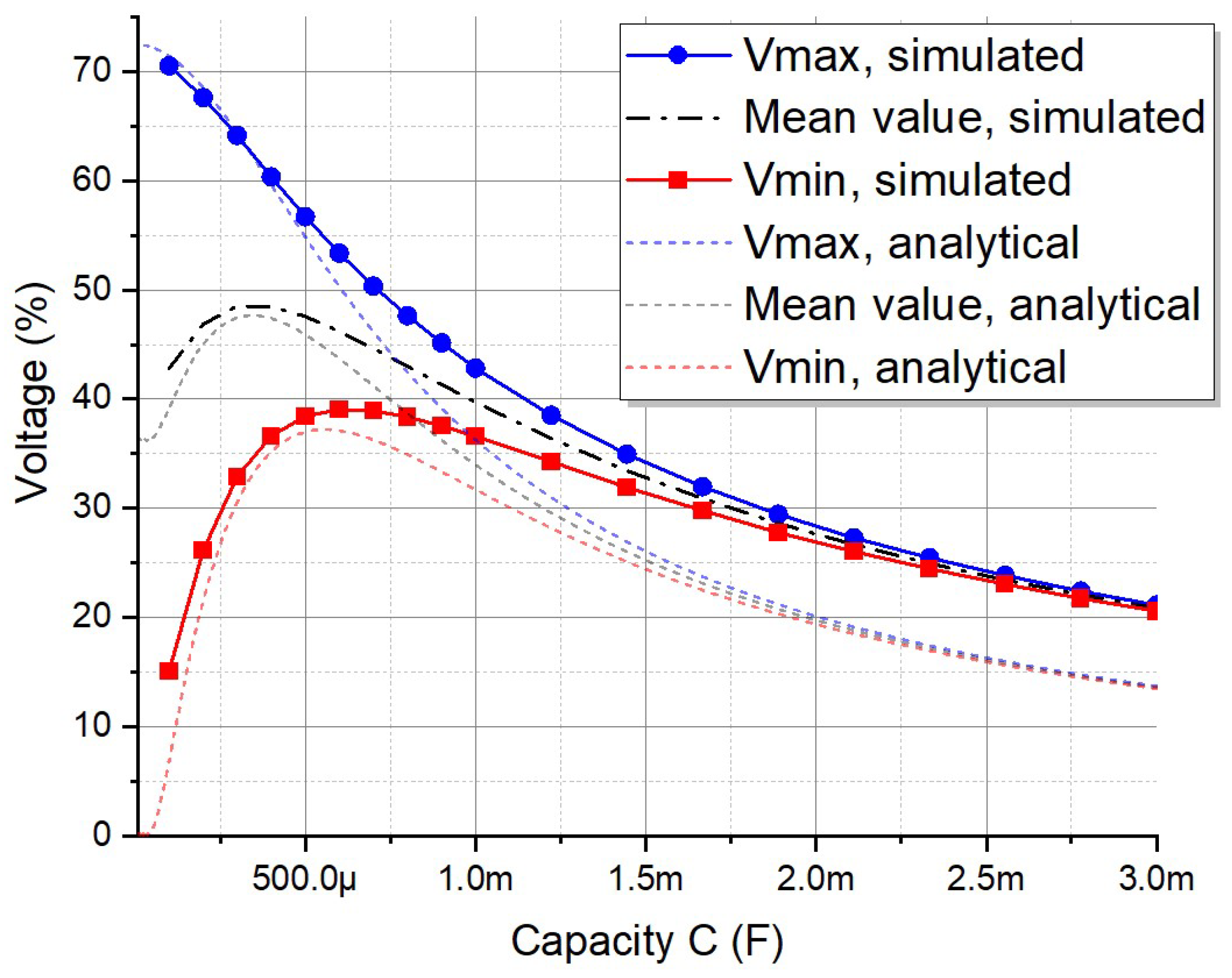
Vmin exhibits a non-linear relationship with the smoothing capacity, featuring a prominent peak value between the first two input signal pulses just above 500 µF. For more comprehensive evaluation, the intersection can be extracted as a projection and plotted on a 2D graph along with Equation (3) for
Vmax (
Figure 3d). The resulting graph shows the dependance of the minimal and maximal voltage values on the smoothing capacity between the first two rectified pulses.
The modeled results reveal that the lowest voltage between the first two rectified pulses initially rises with an increase in the smoothing capacity value, followed by a subsequent decline. In contrast, the highest voltage consistently decreases. This observed trend suggests the presence of an optimal smoothing capacity value, at which the mean rectified voltage reaches its maximum value, indicating the peak performance of the full-bridge circuit.
The proposed model makes an important assumption that the smoothing capacity starts charging from zero. In order for this assumption to hold, it is necessary for the period between the reoccurrence of pulses in the input to be long enough to allow the capacitor to discharge. We assume that the discharge occurs within five time constants of an RC circuit; consequently, the capacity at which the discharge fails to complete can be calculated using Equation (10), where
T is the time between repeated input signal pulses in seconds.
In the case of the input signal used in our study, the pauses between pulses are approximately 0.5 s (as shown in
Figure 1a). Considering a load of 50 Ω, the calculated capacity is found to be 2 mF. This value exceeds the predicted peak capacity (
Figure 3c), indicating that the modeled results are applicable in this scenario.
4. Discussion
To explore the impact of smoothing capacity on the performance of a full-bridge rectifier for intermittent signals, we developed an analytical model that incorporates essential parameters like load resistance, input signal frequency, and circuit losses (e.g., internal resistance of the generator). Our model predicts that, depending on these parameters, the rectifier will deliver the highest minimal voltage
Vmin only at a specific smoothing capacity. Moreover, it enables the attainment of the highest mean value of the rectified voltage, thereby maximizing rectifier efficiency. In contrast, existing analytical models are designed for stable, uninterrupted signal rectification and predict an increase and eventual saturation of the mean rectified voltage with increasing smoothing capacity. For instance, the analytical model proposed in the work [
27], when applied to the same input parameters as our model in
Figure 3, demonstrates a steady increase in mean voltage and a decrease in ripple with increasing capacity (
Figure 12), which is ultimately limited by losses. However, our proposed model reveals a significantly different influence for short and intermittent input signals (
Figure 3d), which are more common for non-inertial mechanical energy harvesters. The proposed model and existing stationary signal models are based on mutually exclusive operating conditions and cannot be directly compared; nevertheless, this demonstrates a significant difference in the influence of smoothing capacity depending on the type of input signal. This difference may have been previously overlooked, primarily because practical applications rarely involve short, intermittent power pulses.
There are several shortcomings of the proposed model. It tends to predict lower voltage values (
Figure 4) and is only applicable to static losses
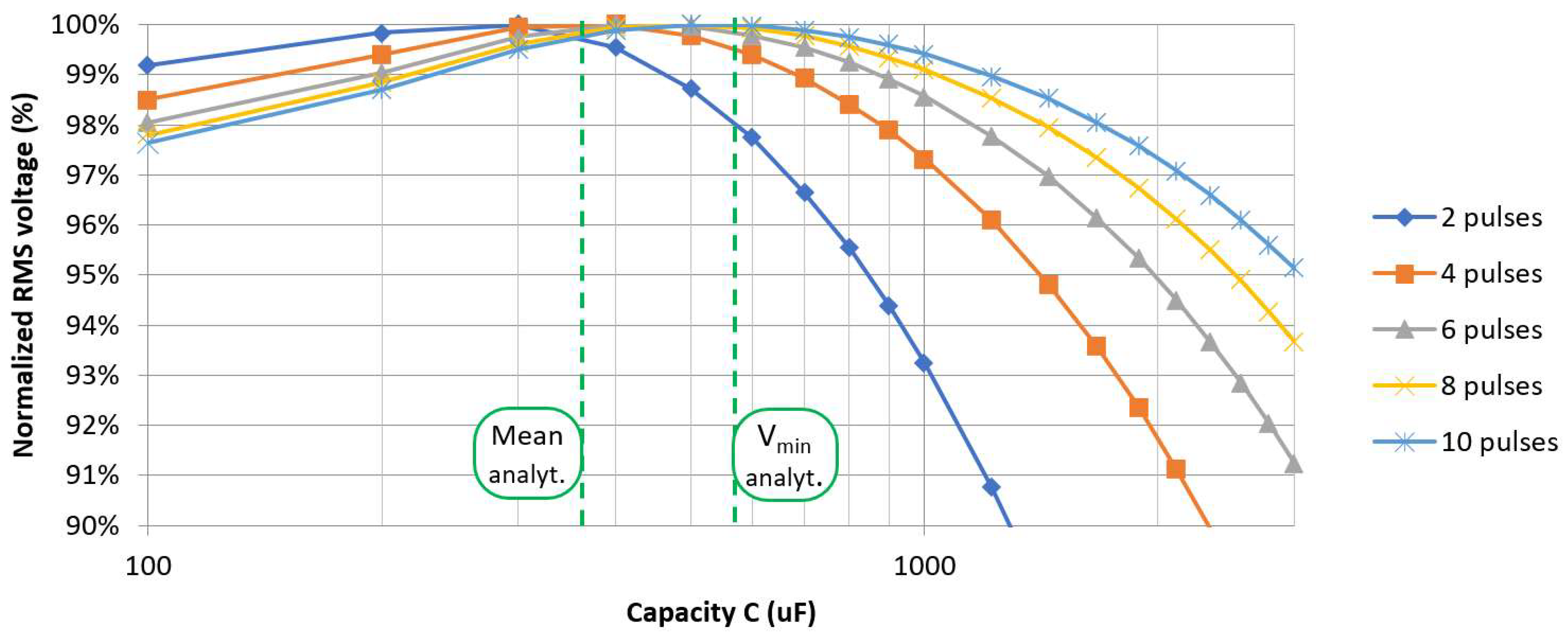
r, but non-linear elements like diodes change their resistance depending on the input signal, meaning their average values might need to be applied to the model. The proposed model focuses solely on predicting the voltage between the first two rectified pulses. Consequently, when a longer input signal is encountered, the displayed peak values gradually flatten out and shift towards higher capacities, as demonstrated in the simulations (
Figure 6). Ultimately, the relationship between the rectified voltage and the smoothing capacity will resemble the predictions of stationary-input models, as illustrated in
Figure 12. The precise number of uninterrupted input signal periods required for this transition is not covered by this study and likely relies on the circuit parameters. In our simulations, a distinct peak value was observed for up to five input periods (
Figure 6). This suggests that the effect encountered at the start of the multi-period signal can persist even in a longer time span, showing its significant impact.
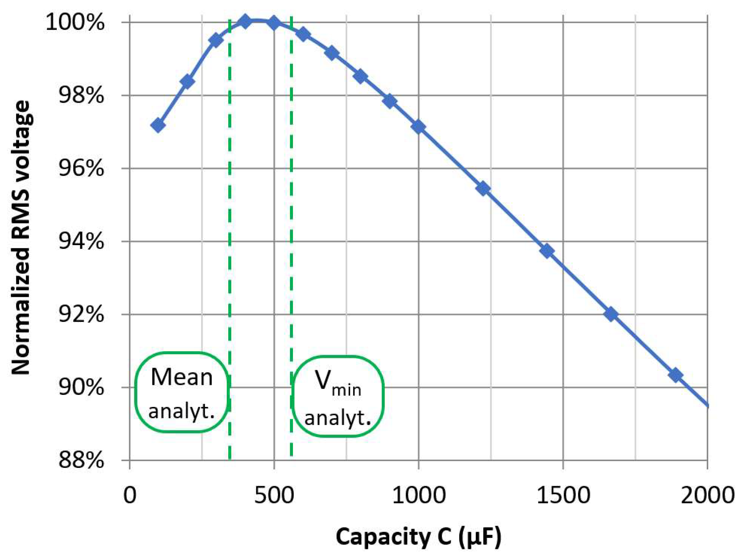
By evaluating the RMS value of the whole rectified signal, the obtained relationship indicated the peak value at the smoothing capacity between the predicted mean and the lowest voltage peak (see
Figure 3d and
Figure 5). Introducing additional losses in the circuit, such as non-ideal rectification elements, and extending the length of the input signals causes this peak capacity value to shift towards either side. However, simulations consistently demonstrated and the practical experiment also confirmed (
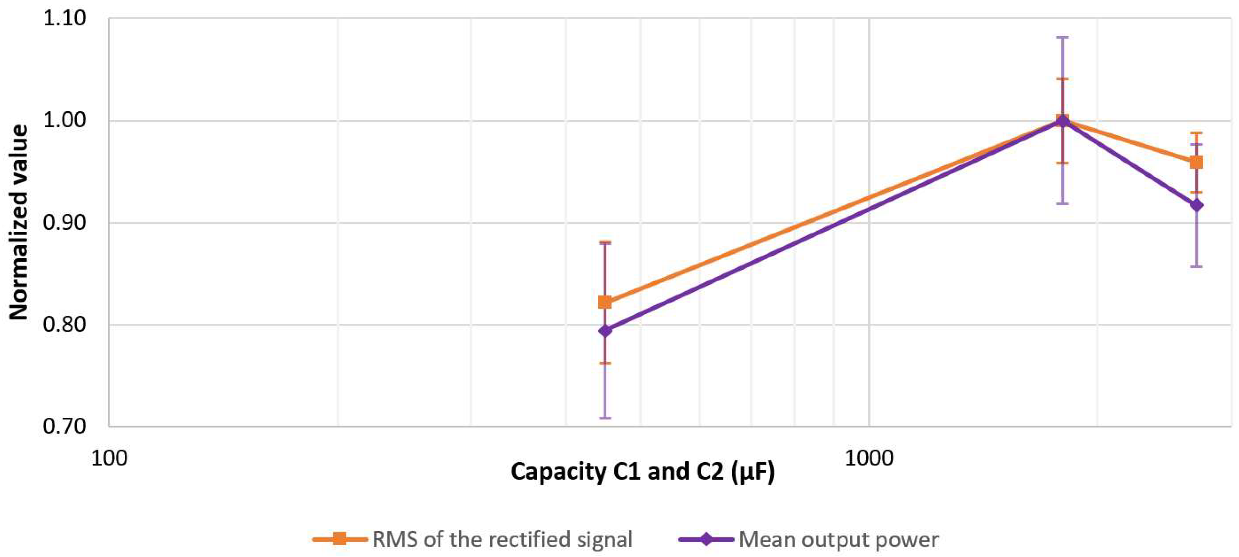
Figure 8) that the peak value predominantly remains within the capacity range defined by the predicted mean and
Vmin voltage peaks, even for an active switching load like a low-voltage converter. This suggests that the modeled results can effectively guide the selection of smoothing capacity for short, intermittent signals. Specifically, if the expected input signal spans several periods, the capacity should be chosen around the predicted
Vmin peak. Alternatively, this predicted region can serve as a guideline for experimental testing, omiting other capacity values and enabling faster identification of the most suitable capacity, for instance, in case of specific and varying input signals.
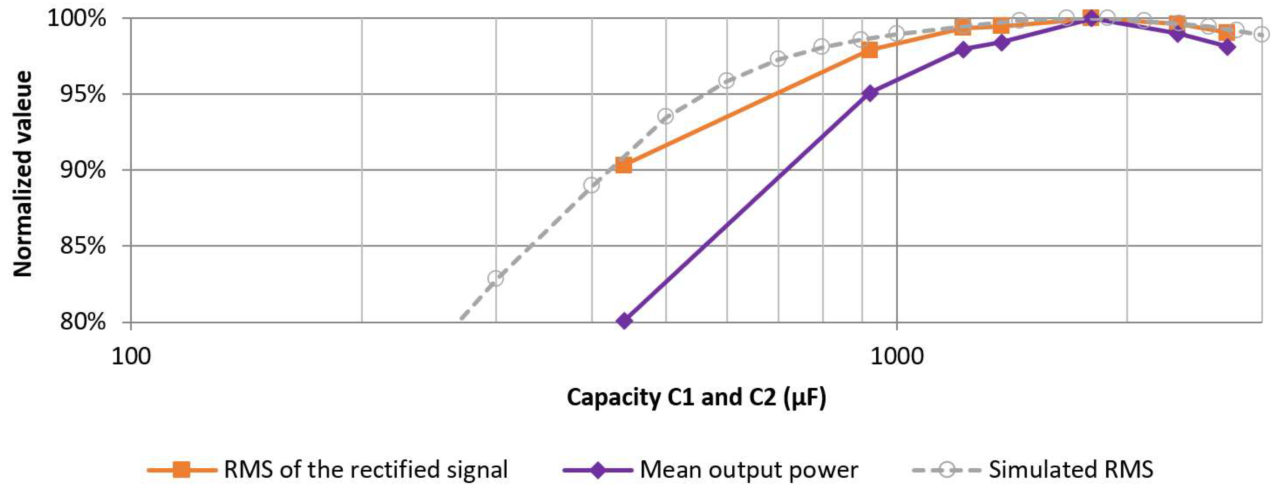
The presence of an optimal capacity for intermittent signals was further confirmed in a voltage multiplier circuit, thereby validating the existence of this relationship across various circuits where capacitors are periodically charged from zero using voltage pulses. To explore this phenomenon in circuit configurations that currently lack analytical models, computer simulations utilizing SPICE models serve as a valuable tool, offering detailed settings and providing matching results with real-life tests (
Figure 10). It is worth mentioning that these simulations can be computationally intensive since they involve calculating full waveforms of the output signal before proceeding with further processing to extract the desired values. Despite the proposed full-bridge model taking certain simplifications, it has been demonstrated to yield results that closely align with the simulations. Furthermore, the graphical solution method employed by the proposed model allows for a rapid attainment of the desired outcome.
It should be noted that active loads may not always exhibit the highest performance at the maximum RMS input (as depicted in
Figure 8 compared to
Figure 10). Presumably, this behavior is attributed to the dependency of the converter efficiency on the input voltage (
Figure 13). Specifically, in the full-bridge experiment (
Section 3.2.1), the highest RMS value recorded was 95 mV, falling on the start of a steep efficiency curve (
Figure 13, EH4205). Consequently, at a lower capacity value, wherein the RMS value had not yet decreased by more than 3%, but
Vmax had notably increased according to the model, and the converter was able to harness the advantages of higher peaks. This, in turn, yielded a higher performance benefit due to the steep efficiency curve with respect to the input voltage. In contrast, the voltage-doubler experiment exhibited an RMS value as high as 470 mV, representing a more stable efficiency region on the curve (
Figure 13, EH4295). Correspondingly, it exhibited the highest performance at the peak of its input RMS voltage, as illustrated in
Figure 10. However, the notably higher RMS value was the result of not only the voltage multiplier but also a higher load value (1 kΩ vs. 50 Ω). This, in turn, decreased the current and subsequently reduced losses in the rectifier elements.
The experimentally obtained results based on an idealized input signal successfully demonstrated the modeled and simulated impact of capacity on rectifier performance (
Section 3.2). However, real-life scenarios often involve variable harvester generation. To address this limitation, an experiment was conducted using an actual human motion energy harvester (
Section 3.3). Repeated measurements revealed a significant variance in the RMS values, reaching up to 10.8%, representing the unstable nature of human motion. Despite this variability, the average values exhibited the expected behavior, with the highest rectified voltage RMS value aligning with the predicted capacity value. The accuracy can be attributed to the fact that the main impact of human motion variations is primarily on the amplitude of the generated signal. As described in Equations (3) and (8) of the proposed model, these variations predominantly affect the magnitude of the voltage, which explains why the capacity prediction remains consistent despite the observed variations, validating the usefulness of capacity optimization for real-life applications.
5. Conclusions
An analytical model was developed to investigate the impact of smoothing capacity on the output voltage of a full-bridge rectifier when operating with short, intermittent signals. It uses input signal frequency, load resistance, and static losses in the circuit, such as the internal resistance of the generator, to determine the trend of achievable voltage on the load based on the smoothing capacity. Notably, an optimal capacity value was identified, which leads to the highest mean voltage on the load, consequently, achieving the highest rectification efficiency. Importantly, the model can be solved graphically, reducing the computational resources otherwise required for detailed circuit simulations. Furthermore, the model showed close approximation of an optimal capacity in the case of multiple-period input signals and non-linear rectification elements.
The existence of an optimal capacity for intermittent signals was further confirmed through simulation conducted on a voltage multiplier circuit, validating that the observed relationship exists across different circuits in which capacitors are periodically charged from zero using voltage pulses. Experimental testing utilizing a generator as a source and a low-voltage step-up converter confirmed the predicted optimal capacity values for both full-bridge and multiplier circuits. Deviating from the optimal smoothing capacity resulted in a decrease in rectified RMS voltage by up to 5% for the full-bridge circuit and 10% for the voltage multiplier circuit, which in return significantly decreased the output power of different converters by up to 33% and 20%. The real-world experiments conducted with a human motion energy harvester and voltage multiplier demonstrated an average loss of RMS voltage for non-optimal capacities of up to 15% and substantial performance degradation of the low-voltage converter by at least 20%, evidencing significant improvements of the capacity-optimized rectifier even in varying generation environments.


