
Real-Time Implementation of an Optimized Model Predictive Control for a 9-Level CSC Inverter in Grid-Connected Mode


 , ,
, ,  and
and 
Abstract
:1. Introduction
2. CSC Topology and Mathematical Modelling
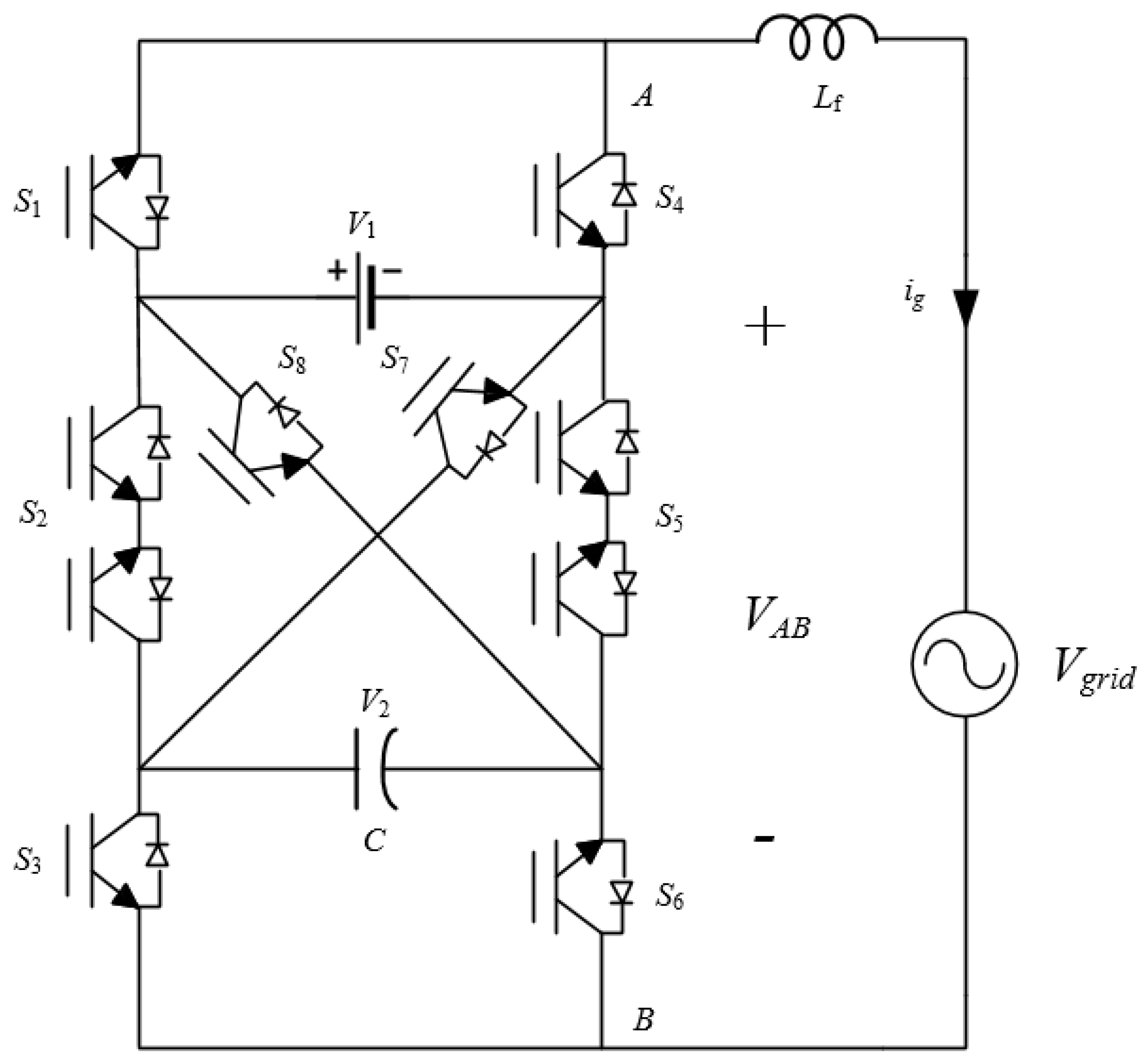
2.1. CSC Topology
2.2. Modelling
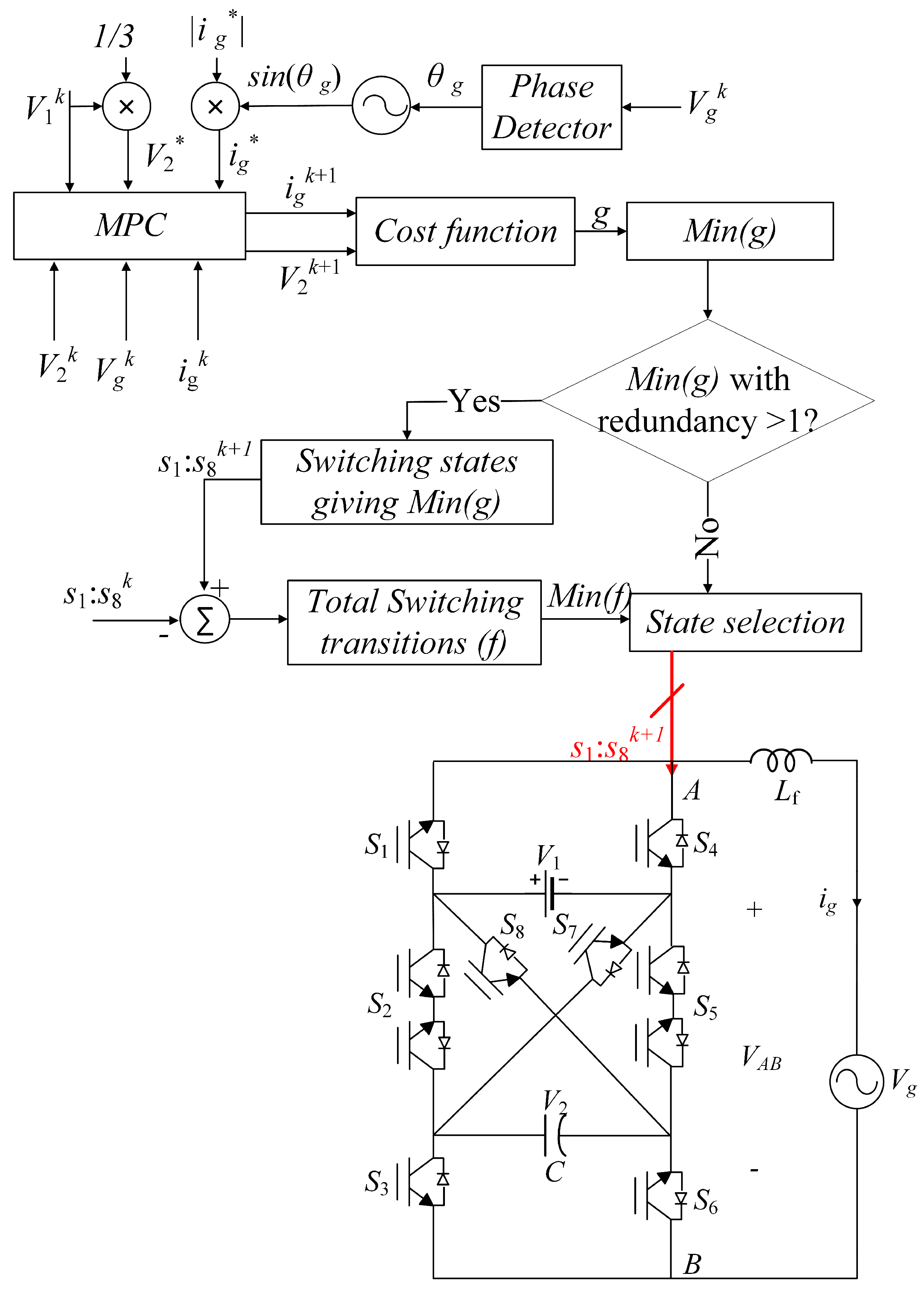
3. Control Scheme
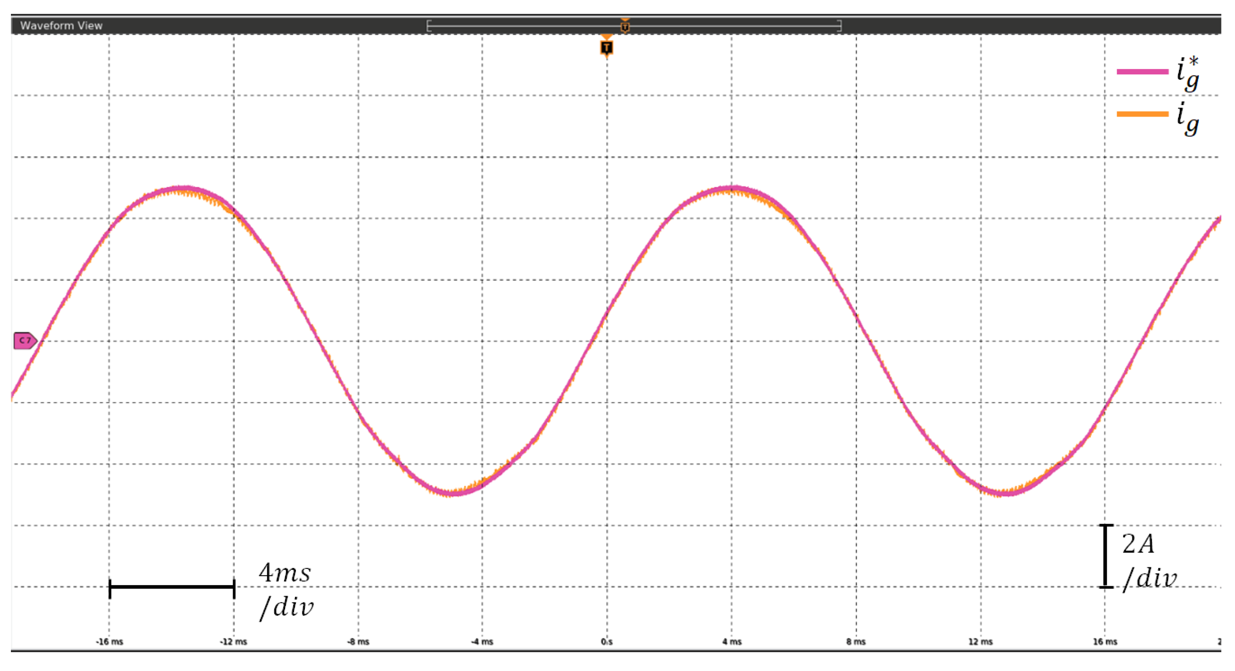
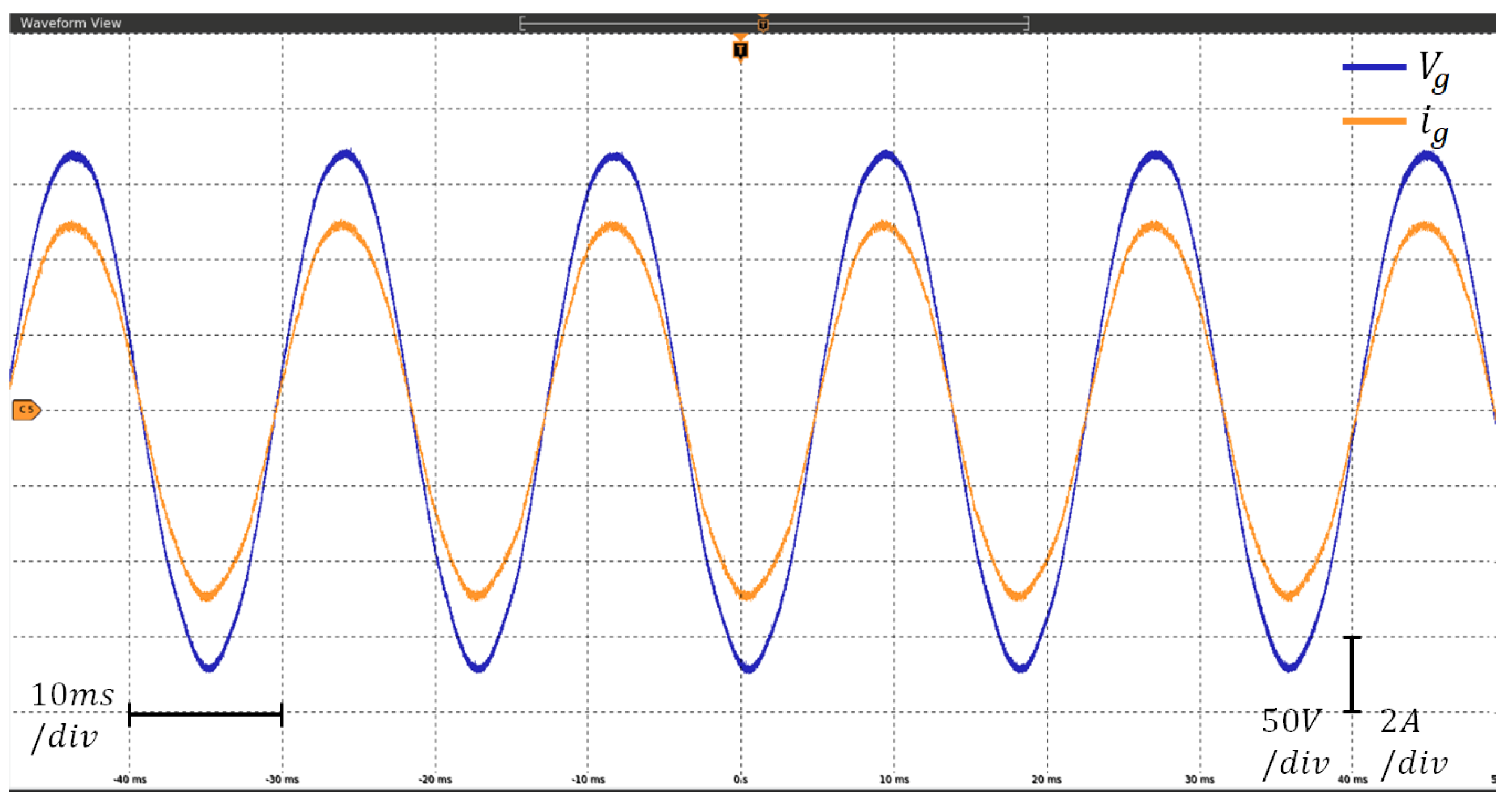
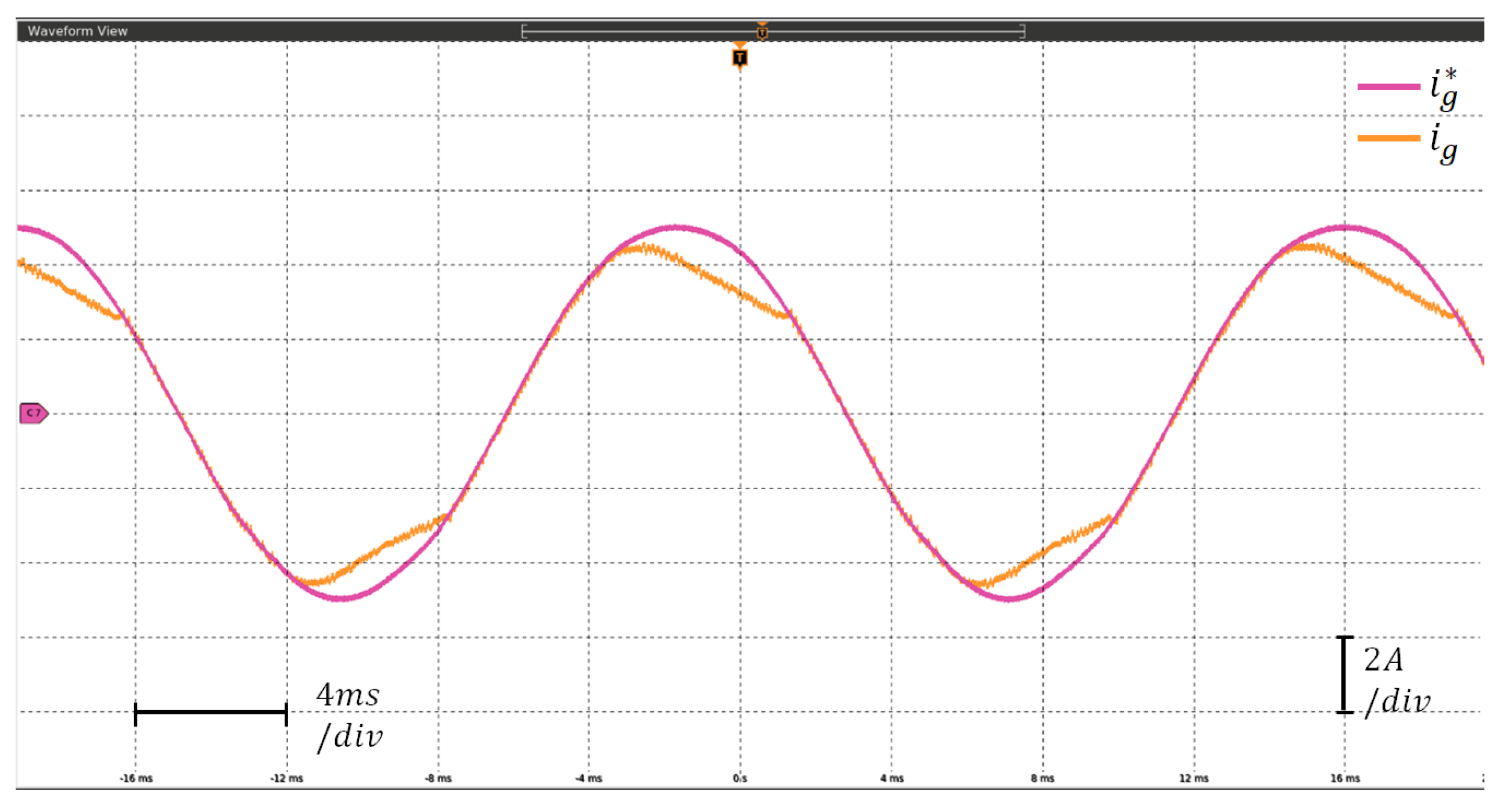
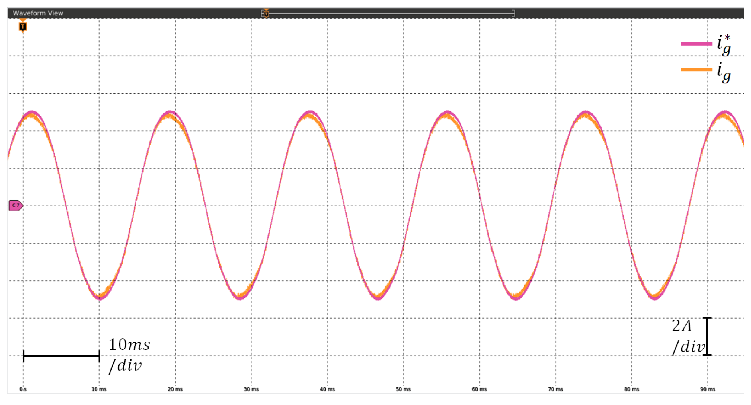
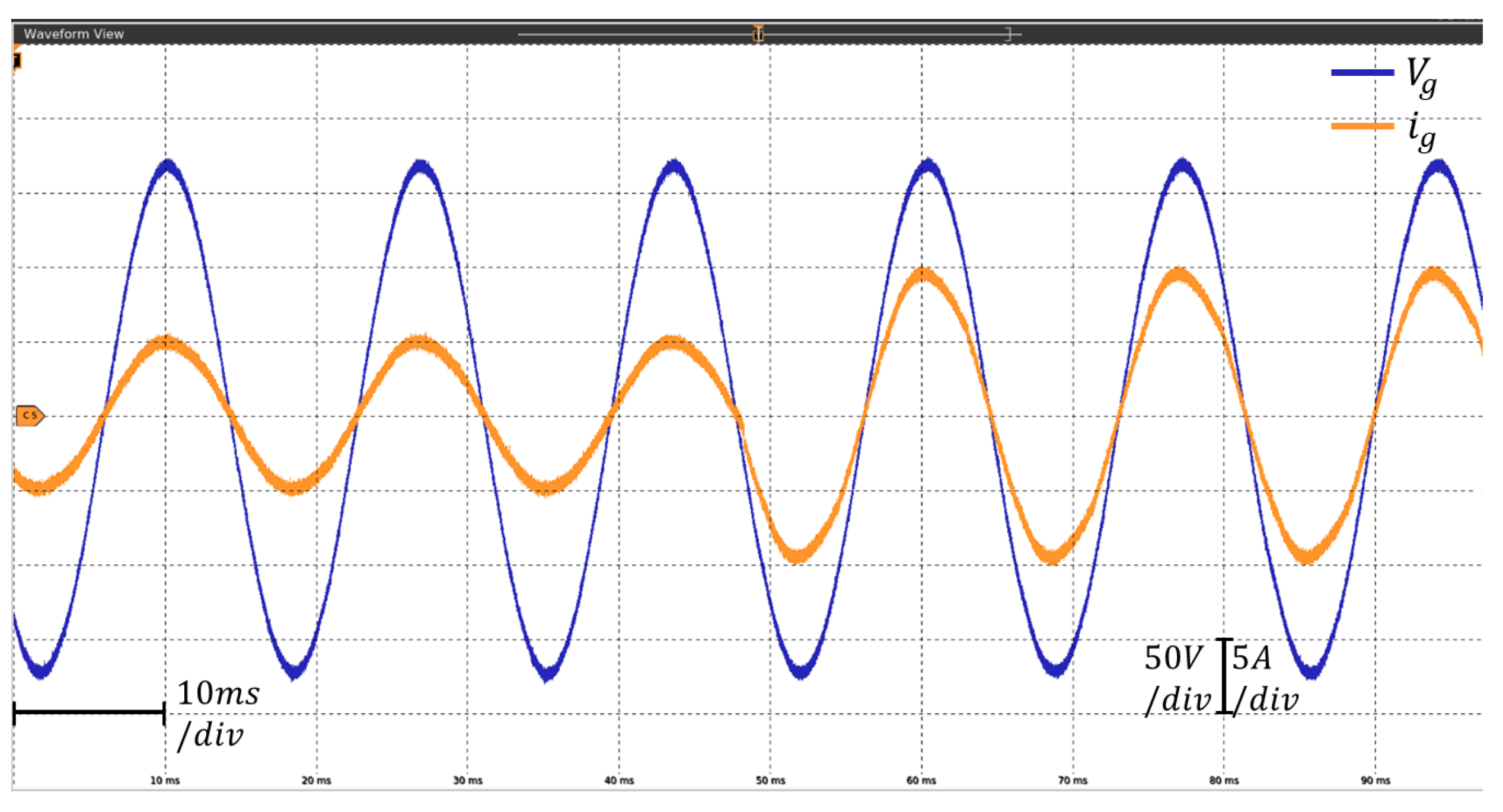
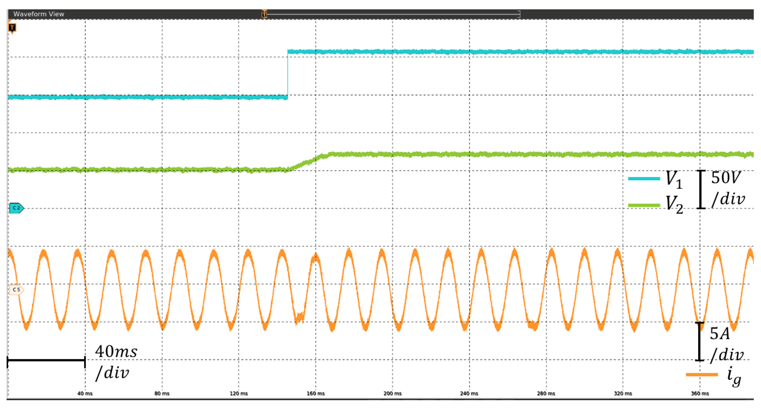
4. Results and Discussion
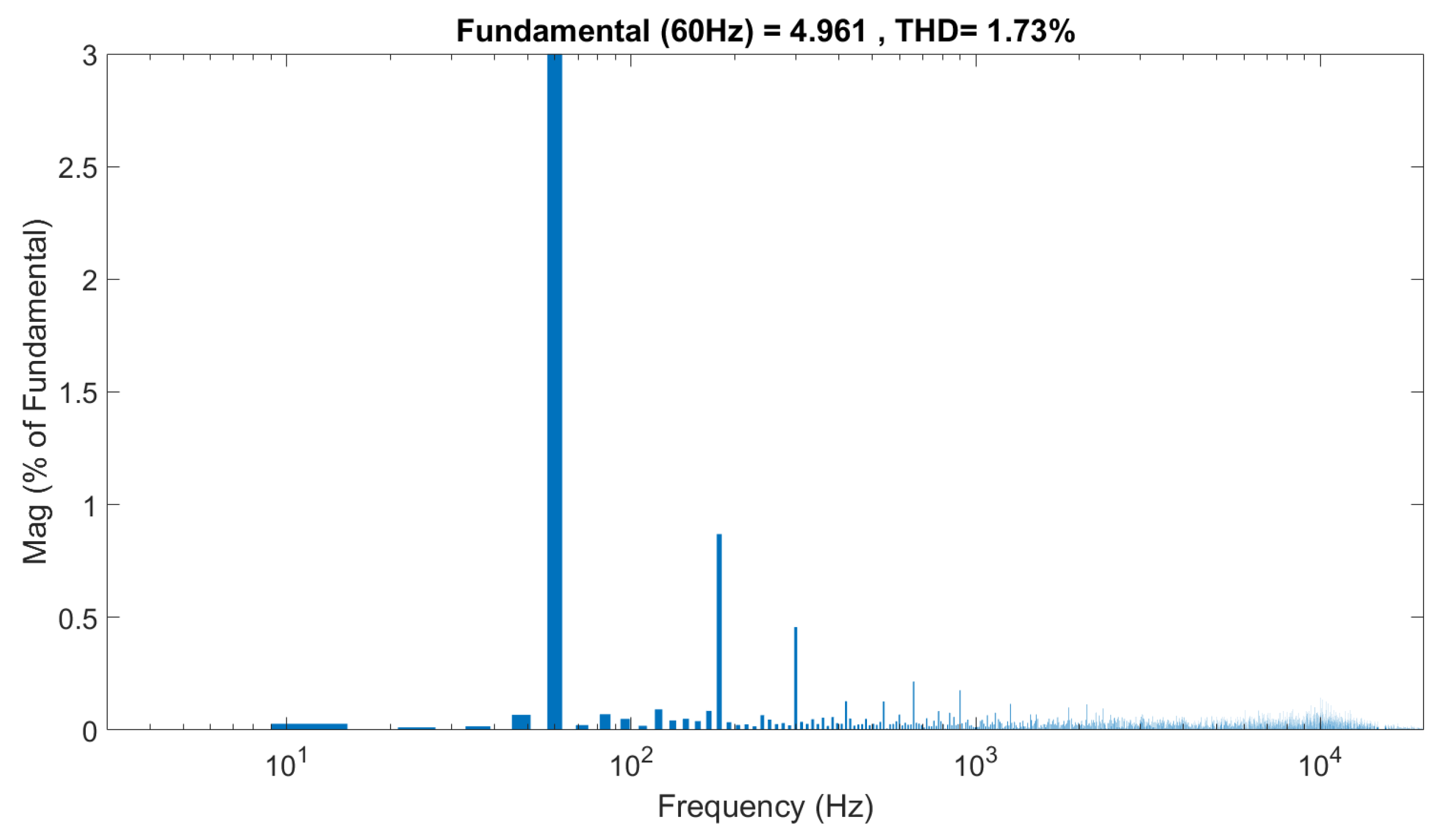
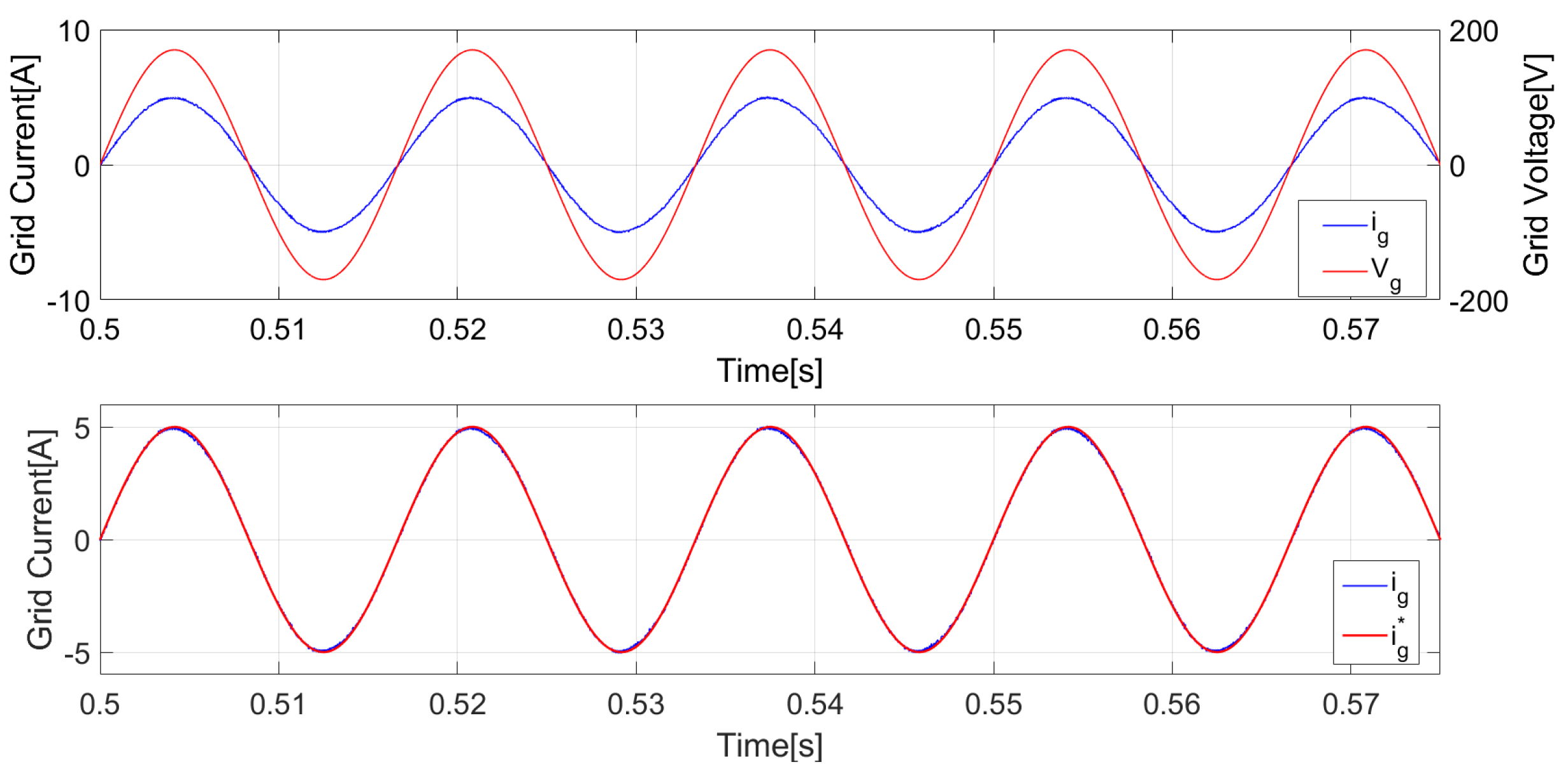
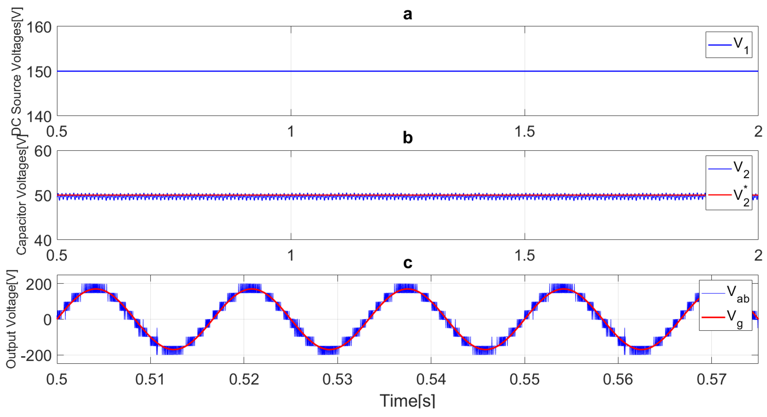
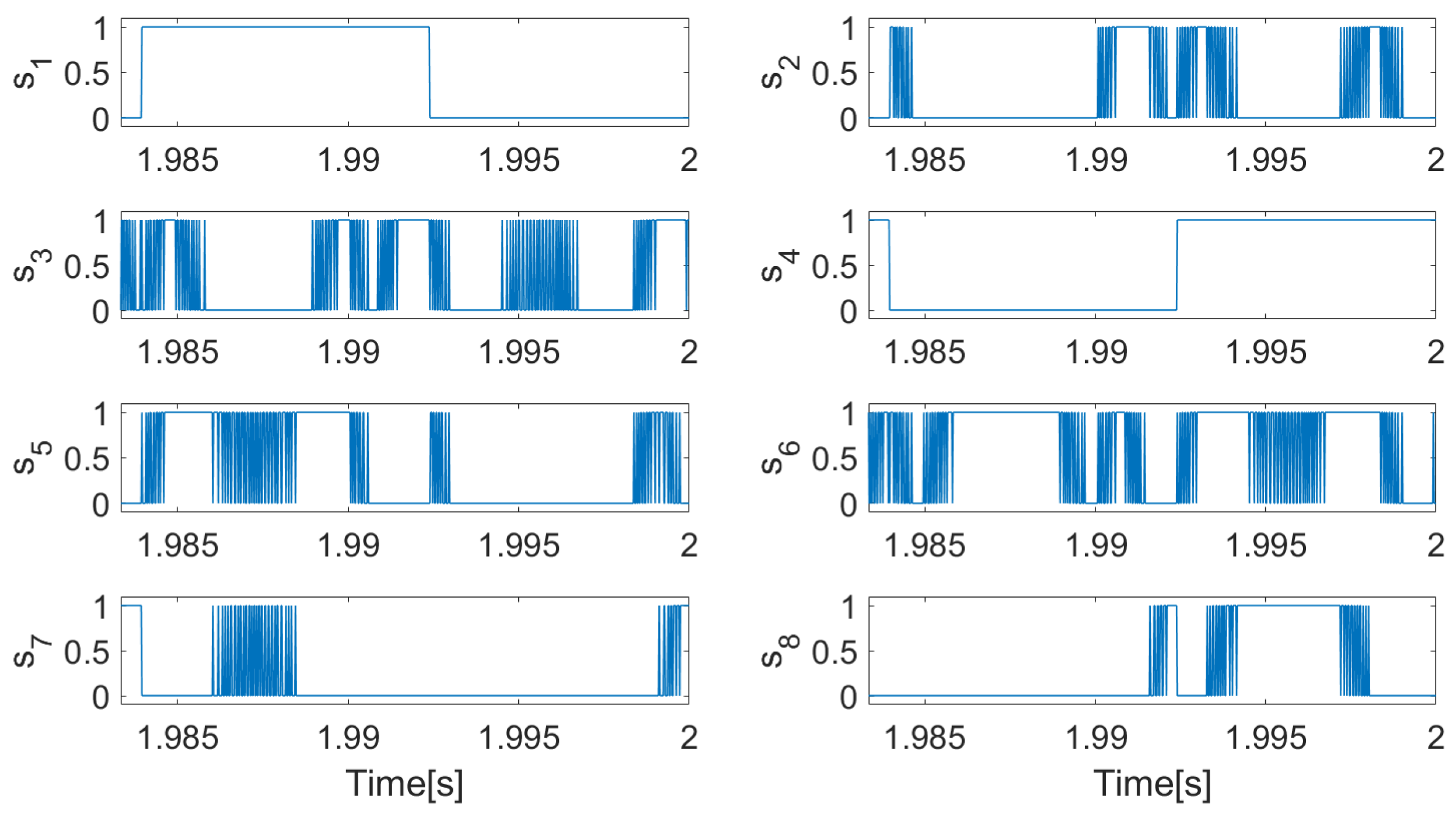
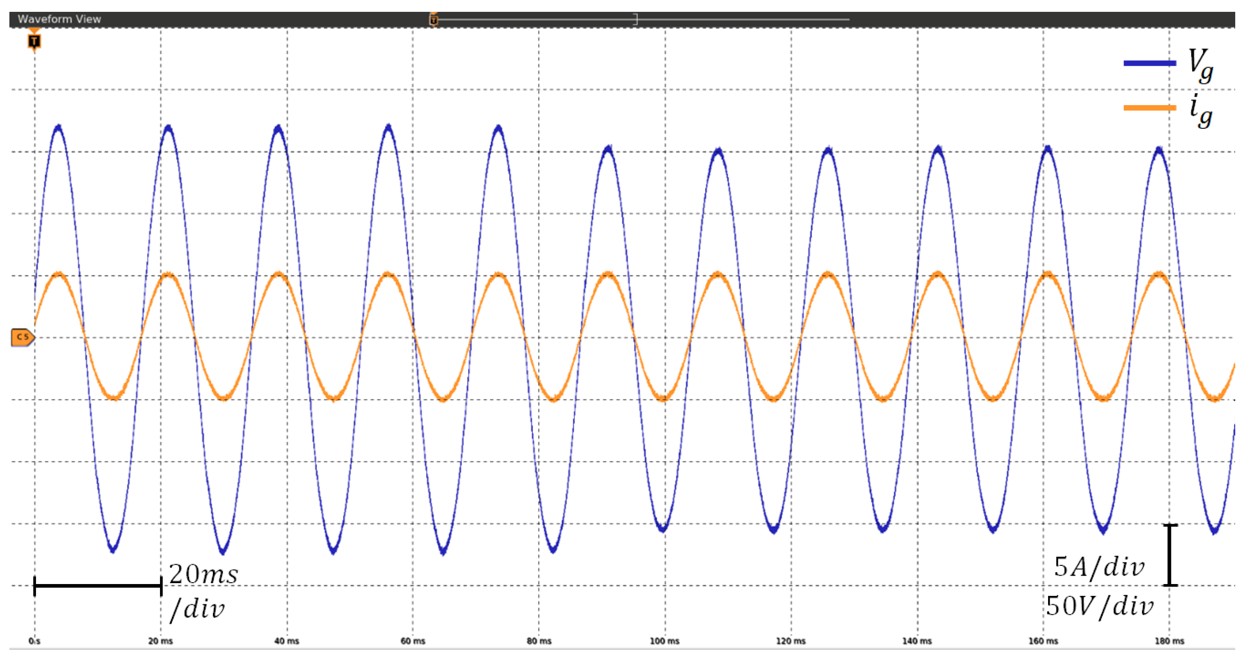
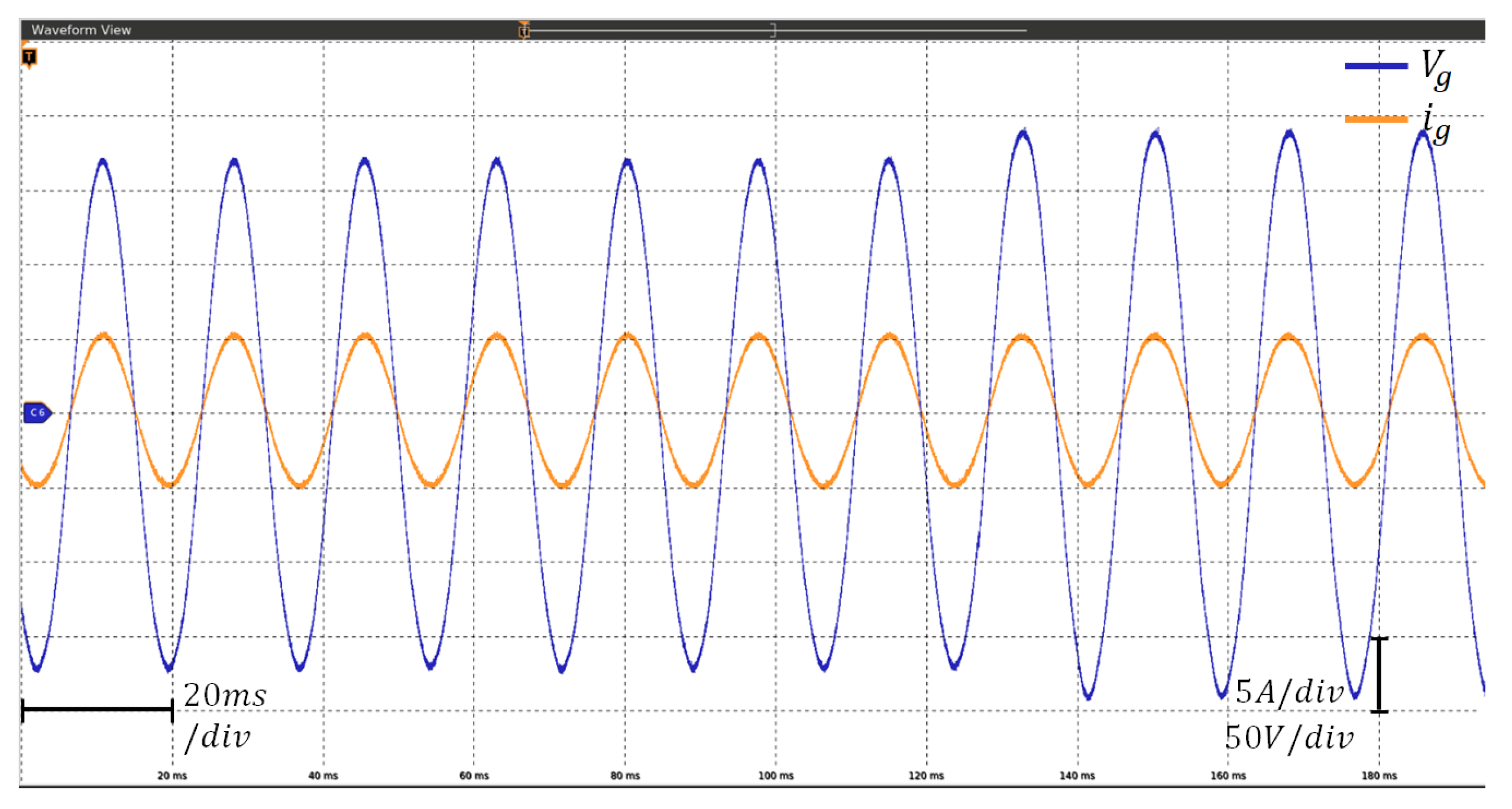
4.1. Simulation Results
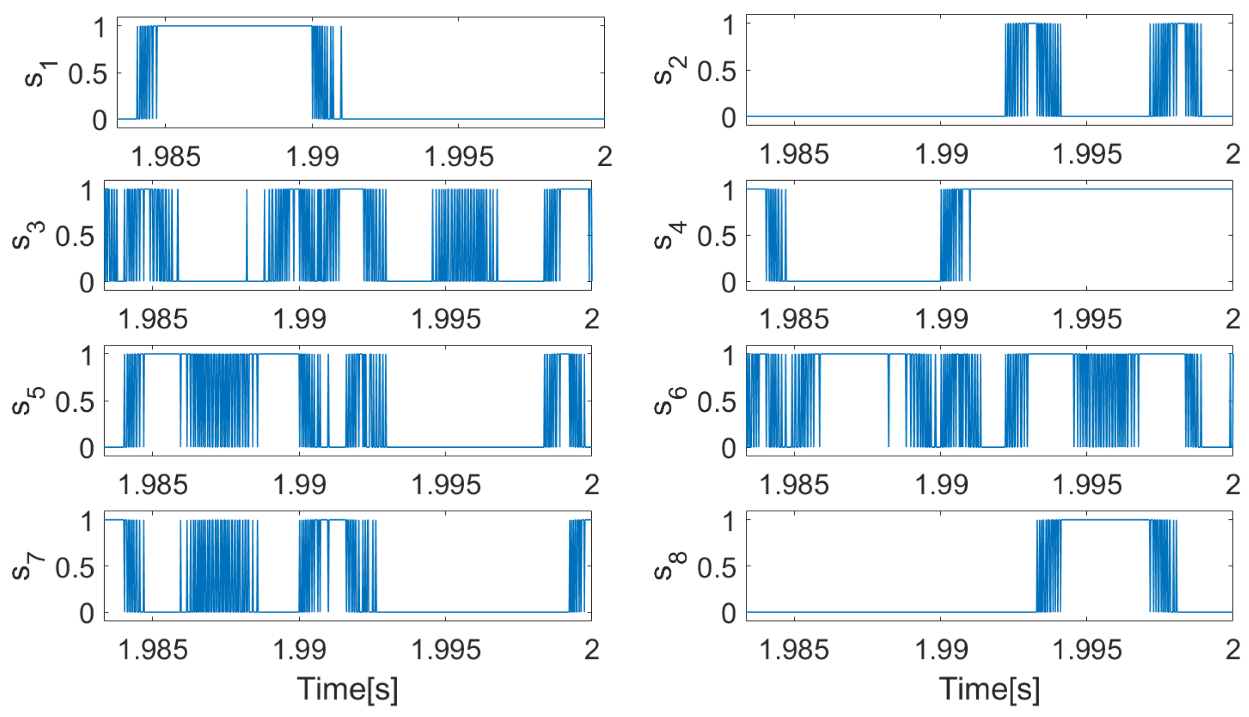
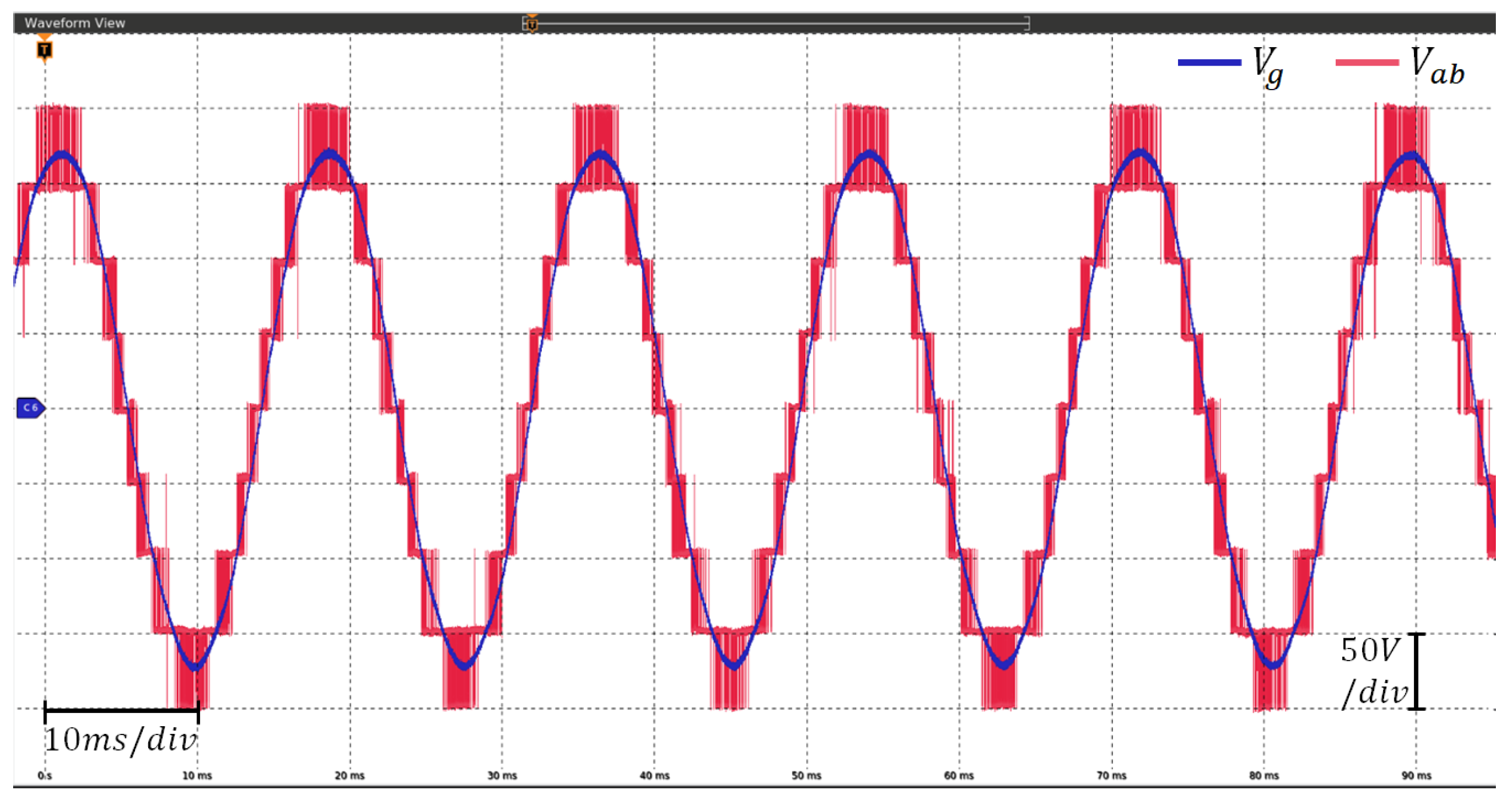
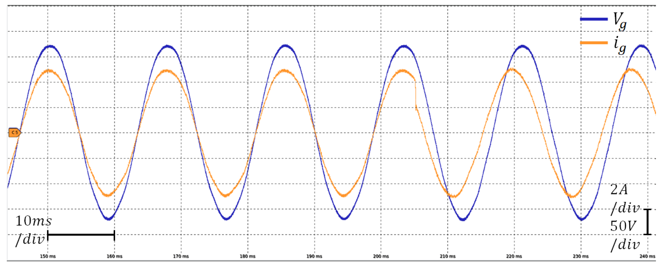
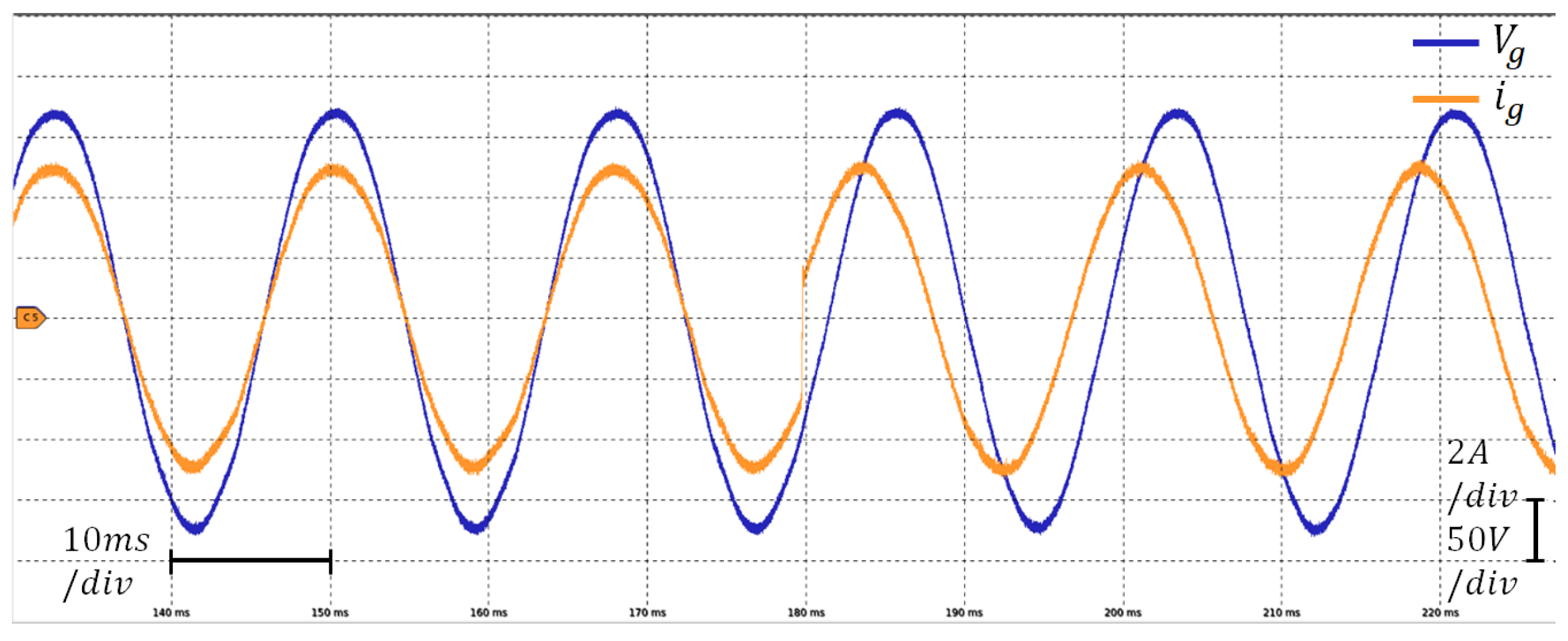
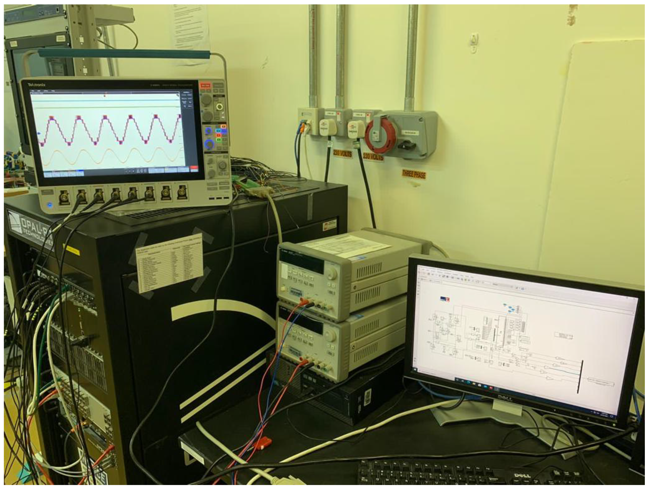
4.2. Implementation Results
5. Conclusions
Author Contributions
Funding
Institutional Review Board Statement
Informed Consent Statement
Data Availability Statement
Conflicts of Interest
Abbreviations
| MLI | Multilevel Inverter |
| THD | Total harmonic distortion |
| CSC | Crossover switches Cell |
| FCS-MPC | Finite control set-model predictive control |
| (i 1 to 8) | CSC switches |
| DC link voltage | |
| Capacitor voltage | |
| CSCoutput Voltage | |
| Grid voltage | |
| Grid current | |
| Sampling time |
References
- IRENA. Renewable Capacity Statistics 2021 International Renewable Energy Agency (IRENA); IRENA: Abu Dhabi, United Arab Emirates, 2021. [Google Scholar]
- Alluhaybi, K.; Batarseh, I.; Hu, H. Comprehensive Review and Comparison of Single-Phase Grid-Tied Photovoltaic Microinverters. IEEE J. Emerg. Select. Top. Power Electron. 2020, 8, 1310–1329. [Google Scholar] [CrossRef]
- Edwin, F.; Xiao, W.; Khadkikar, V. Topology review of single phase grid-connected module integrated converters for PV applications. In Proceedings of the IECON 2012—38th Annual Conference on IEEE Industrial Electronics Society, Montreal, QC, Canada, 25–28 October 2012; pp. 821–827. [Google Scholar]
- Chaudhary, S.; Ahmad, Z.; Singh, S.N. Single Phase Grid Interactive Solar Photovoltaic Inverters: A Review. In Proceedings of the 2018 National Power Engineering Conference (NPEC), Madurai, India, 9–10 March 2018; pp. 1–6. [Google Scholar]
- Kjaer, S.B.; Pedersen, J.K.; Blaabjerg, F. A review of single-phase grid-connected inverters for photovoltaic modules. IEEE Trans. Ind. Appl. 2005, 41, 1292–1306. [Google Scholar] [CrossRef]
- Bana, P.R.; Panda, K.P.; Naayagi, R.T.; Siano, P.; Panda, G. Recently Developed Reduced Switch Multilevel Inverter for Renewable Energy Integration and Drives Application: Topologies, Comprehensive Analysis and Comparative Evaluation. IEEE Access 2019, 7, 54888–54909. [Google Scholar] [CrossRef]
- Abu-Rub, H.; Holtz, J.; Rodriguez, J.; Baoming, G. Medium-Voltage Multilevel Converters—State of the Art, Challenges, and Requirements in Industrial Applications. IEEE Trans. Ind. Electron. 2010, 57, 2581–2596. [Google Scholar] [CrossRef]
- Ebrahimi, J.; Babaei, E.; Gharehpetian, G.B. A New Topology of Cascaded Multilevel Converters With Reduced Number of Components for High-Voltage Applications. IEEE Trans. Power Electron. 2011, 26, 3109–3118. [Google Scholar] [CrossRef]
- Jannati, O.; Mohammad, R.; Ebrahim, S.; Sajad, N.-R. Creative design of symmetric multilevel converter to enhance the circuit’s performance. IET Power Electron. 2015, 8, 96–102. [Google Scholar] [CrossRef]
- Malinowski, M.; Gopakumar, K.; Rodriguez, J.; Pérez, M.A. A Survey on Cascaded Multilevel Inverters. IEEE Trans. Ind. Electron. 2010, 57, 2197–2206. [Google Scholar] [CrossRef]
- Trabelsi, M.; Vahedi, H.; Abu-Rub, H. Review on Single-DC-Source Multilevel Inverters: Topologies, Challenges, Industrial Applications, and Recommendations. IEEE Open J. Ind. Electron. Soc. 2021, 2, 112–127. [Google Scholar] [CrossRef]
- Ounejjar, Y.; Al-Haddad, K.; Gregoire, L. Packed U Cells Multilevel Converter Topology: Theoretical Study and Experimental Validation. IEEE Trans. Ind. Electron. 2011, 58, 1294–1306. [Google Scholar] [CrossRef]
- Vahedi, H.; Trabelsi, M. Single-DC-Source Multilevel Inverters; Springer Nature: Cham, Switzerland, 2019; ISBN 978-3-030-15252-9. [Google Scholar] [CrossRef]
- Vahedi, H.; Al-Haddad, K.; Ounejjar, Y. Crossover Switches Cell (CSC): A new multilevel inverter topology with maximum voltage levels and minimum DC sources. In Proceedings of the IECON 2013-39th Annual Conference of the IEEE Industrial Electronics Society, Vienna, Austria, 10–13 November 2013; pp. 54–59. [Google Scholar]
- Nho, N.V.; Youn, M.J. Comprehensive study on space-vector-PWM and carrier-based-PWM correlation in multilevel invertors. IEE Proc. Electr. Power Appl. 2006, 153, 149–158. [Google Scholar] [CrossRef]
- Valderrama, G.E.; Guzman, G.V.; Pool-Mazún, E.I.; Martinez-Rodriguez, P.R.; Lopez-Sanchez, M.J.; Zuñiga, J.M.S. A Single-Phase Asymmetrical T-Type Five-Level Transformerless PV Inverter. IEEE J. Emerg. Select. Top. Power Electron. 2018, 6, 140–150. [Google Scholar] [CrossRef]
- Selvaraj, J.; Rahim, N.A. Multilevel Inverter For Grid-Connected PV System Employing Digital PI Controller. IEEE Trans. Ind. Electron. 2009, 56, 149–158. [Google Scholar] [CrossRef]
- Rodriguez, J.; Lai, J.-S.; Peng, F.Z. Multilevel inverters: A survey of topologies, controls, and applications. IEEE Trans. Ind. Electron. 2002, 49, 724–738. [Google Scholar] [CrossRef] [Green Version]
- Fri, A.; Bachtiri, R.E.; Elghzizal, A. Adaptive Control of a Multilevel Inverter (5L) Connected to the Single Phase Electrical Grid. In Proceedings of the 2018 6th International Renewable and Sustainable Energy Conference (IRSEC), Rabat, Morocco, 5–8 December 2018; pp. 1–6. [Google Scholar]
- Foito, D.; Pires, V.F.; Cordeiro, A.; Silva, J.F. Sliding Mode Vector Control of Grid-Connected PV Multilevel Systems Based on Triple Three-Phase Two-Level Inverters. In Proceedings of the 2020 9th International Conference on Renewable Energy Research and Application (ICRERA), Glasgow, UK, 27–30 September 2020; pp. 399–404. [Google Scholar]
- Revana, G.; Kota, V.R. Closed loop artificial neural network controlled PV based cascaded boost five-level inverter system. In Proceedings of the 2017 International Conference on Green Energy and Applications (ICGEA), Singapore, 25–27 March 2017; pp. 11–17. [Google Scholar]
- Cecati, C.; Ciancetta, F.; Siano, P. A Multilevel Inverter for Photovoltaic Systems With Fuzzy Logic Control. IEEE Trans. Ind. Electron. 2010, 57, 4115–4125. [Google Scholar] [CrossRef]
- Kouro, S.; Cortes, P.; Vargas, R.; Ammann, U.; Rodriguez, J. Model Predictive Control—A Simple and Powerful Method to Control Power Converters. IEEE Trans. Ind. Electron. 2009, 56, 1826–1838. [Google Scholar] [CrossRef]
- Richter, S.; Mariéthoz, S.; Morari, M. High-speed online MPC based on a fast gradient method applied to power converter control. In Proceedings of the 2010 American Control Conference, Baltimore, MD, USA, 30 June–2 July 2010; pp. 4737–4743. [Google Scholar]
- Trabelsi, M.; Retif, J.M.; Lin, S.X.; Brun, X.; Morel, F.; Bevilacqua, P. Hybrid control of a three-cell converter associated to an inductive load. In Proceedings of the 2008 IEEE Power Electronics Specialists Conference, Rhodes, Greece, 15–19 June 2008; pp. 3519–3525. [Google Scholar]
- Trabelsi, M.; Bayhan, S.; Ghazi, K.A.; Abu-Rub, H.; Ben-Brahim, L. Finite-Control-Set Model Predictive Control for Grid-Connected Packed-U-Cells Multilevel Inverter. IEEE Trans. Ind. Electron. 2016, 63, 7286–7295. [Google Scholar] [CrossRef]
- Trabelsi, M.; Bayhan, S.; Refaat, S.S.; Abu-Rub, H.; Ben-Brahim, L. Multi-objective model predictive control for grid-tied 15-level packed U cells inverter. In Proceedings of the 2016 18th European Conference on Power Electronics and Applications (EPE’16 ECCE Europe), Karlsruhe, Germany, 5–9 September 2016; pp. 1–7. [Google Scholar]
- Karamanakos, P.; Geyer, T. Guidelines for the design of finite control set model predictive controllers. IEEE Trans. Power Electron. 2019, 35, 7434–7450. [Google Scholar] [CrossRef]
- Rodriguez, J. State of the Art of Finite Control Set Model Predictive Control in Power Electronics. IEEE Trans. Ind. Inform. 2013, 9, 1003–1016. [Google Scholar] [CrossRef]
- Rodriguez, J.; Pontt, J.; Silva, C.A.; Correa, P.; Lezana, P.; Cortés, P.; Ammann, U. Predictive current control of a voltage source inverter. IEEE Trans. Ind. Electron. 2007, 54, 495–503. [Google Scholar] [CrossRef]
- Kukrer, O. Discrete-time current control of voltage-fed three-phase PWM inverters. IEEE Trans. Power Electron. 1996, 11, 260–269. [Google Scholar] [CrossRef]
- Alquennah, A.N.; Trabelsi, M.; Vahedi, H. FCS-MPC of Grid-Connected 9-Level Crossover Switches Cell Inverter. In Proceedings of the IECON 2020 the 46th Annual Conference of the IEEE Industrial Electronics Society, Singapore, 18–21 October 2020; pp. 2430–2435. [Google Scholar]
- Zhou, Z.; Khanniche, M.S.; Igic, P.; Kong, S.T.; Towers, M.; Mawby, P.A. A fast power loss calculation method for long real-time thermal simulation of IGBT modules for a three-phase inverter system. In Proceedings of the 2005 European Conference on Power Electronics and Applications, Dresden, Germany, 11–14 September 2005; pp. 9–10. [Google Scholar]
- Kim, T.; Kang, D.; Lee, Y.; Hyun, D. The analysis of conduction and switching losses in multi-level inverter system. In Proceedings of the 2001 IEEE 32nd Annual Power Electronics Specialists Conference (IEEE Cat. No. 01CH37230), Vancouver, BC, Canada, 17–21 June 2001; pp. 1363–1368. [Google Scholar]
- Krarti, M. Chapter 4-Utility Rate Structures and Grid Integration, Optimal Design and Retrofit of Energy Efficient Buildings; Butterworth-Heinemann: Oxford, UK, 2018; pp. 189–245. [Google Scholar]


| (V) | Cell Capacitor | |||||||||
|---|---|---|---|---|---|---|---|---|---|---|
| 1 | 0 | 0 | 0 | 0 | 1 | 1 | 0 | 200 | Charged | |
| 1 | 0 | 0 | 0 | 1 | 1 | 0 | 0 | 150 | Bypassed | |
| 1 | 0 | 1 | 0 | 0 | 0 | 1 | 0 | 150 | Bypassed | |
| 1 | 0 | 1 | 0 | 1 | 0 | 0 | 0 | 100 | Discharged | |
| 0 | 0 | 0 | 1 | 0 | 1 | 1 | 0 | 50 | Charged | |
| 1 | 1 | 0 | 0 | 0 | 1 | 0 | 0 | 50 | Charged | |
| 0 | 0 | 1 | 1 | 0 | 0 | 1 | 0 | 0 | 0 | Bypassed |
| 1 | 1 | 1 | 0 | 0 | 0 | 0 | 0 | 0 | 0 | Bypassed |
| 0 | 0 | 0 | 1 | 1 | 1 | 0 | 0 | 0 | 0 | Bypassed |
| 1 | 0 | 0 | 0 | 0 | 1 | 0 | 1 | 0 | 0 | Bypassed |
| 0 | 0 | 1 | 1 | 1 | 0 | 0 | 0 | −50 | Discharged | |
| 1 | 0 | 1 | 0 | 0 | 0 | 0 | 1 | −50 | Discharged | |
| 0 | 1 | 0 | 1 | 0 | 1 | 0 | 0 | −100 | Charged | |
| 0 | 0 | 0 | 1 | 0 | 1 | 0 | 1 | −150 | Bypassed | |
| 0 | 1 | 1 | 1 | 0 | 0 | 0 | 0 | −150 | Bypassed | |
| 0 | 0 | 1 | 1 | 0 | 0 | 0 | 1 | −200 | Discharged |
| Parameters | Value |
|---|---|
| Fundamental frequency | 60 Hz |
| Sampling time | s |
| Grid voltage peak | 170 V |
| Grid current peak | 5 A |
| DC source voltage | 150 V |
| Capacitor voltage | 50 V |
| Capacitor C | F |
| Filtering inductor | 6 mH |
| Current weighting factor | 10 |
| Voltage weighting factor | 5 |
Publisher’s Note: MDPI stays neutral with regard to jurisdictional claims in published maps and institutional affiliations. |
© 2021 by the authors. Licensee MDPI, Basel, Switzerland. This article is an open access article distributed under the terms and conditions of the Creative Commons Attribution (CC BY) license (https://creativecommons.org/licenses/by/4.0/).
Share and Cite
Alquennah, A.N.; Trabelsi, M.; Rayane, K.; Vahedi, H.; Abu-Rub, H. Real-Time Implementation of an Optimized Model Predictive Control for a 9-Level CSC Inverter in Grid-Connected Mode. Sustainability 2021, 13, 8119. https://doi.org/10.3390/su13158119
Alquennah AN, Trabelsi M, Rayane K, Vahedi H, Abu-Rub H. Real-Time Implementation of an Optimized Model Predictive Control for a 9-Level CSC Inverter in Grid-Connected Mode. Sustainability. 2021; 13(15):8119. https://doi.org/10.3390/su13158119
Chicago/Turabian StyleAlquennah, Alamera Nouran, Mohamed Trabelsi, Khaled Rayane, Hani Vahedi, and Haitham Abu-Rub. 2021. "Real-Time Implementation of an Optimized Model Predictive Control for a 9-Level CSC Inverter in Grid-Connected Mode" Sustainability 13, no. 15: 8119. https://doi.org/10.3390/su13158119
APA StyleAlquennah, A. N., Trabelsi, M., Rayane, K., Vahedi, H., & Abu-Rub, H. (2021). Real-Time Implementation of an Optimized Model Predictive Control for a 9-Level CSC Inverter in Grid-Connected Mode. Sustainability, 13(15), 8119. https://doi.org/10.3390/su13158119