Article

Evaluation and Selection of Materials for Particulate Matter MEMS Sensors by Using Hybrid MCDM Methods

1
Department of Industrial Education, National Taiwan Normal University, Taipei 106, Taiwan
2
Institute of Management of Technology, National Chiao-Tung University, 1001 University Road, Hsinchu 300, Taiwan
3
Department of Computer Science and Information Engineering, National Taiwan Normal University, Taipei 106, Taiwan
4
Department of Electrical Engineering, National Taiwan University, Taipei 106, Taiwan
5
Department of Mechanical Engineering, National Taipei University of Technology, Taipei 106, Taiwan
*
Author to whom correspondence should be addressed.
Sustainability 2018, 10(10), 3451; https://doi.org/10.3390/su10103451
Submission received: 31 July 2018 / Revised: 11 September 2018 / Accepted: 19 September 2018 / Published: 27 September 2018

Abstract

:
Air pollution poses serious problems as global industrialization continues to thrive. Since air pollution has grave impacts on human health, industry experts are starting to fathom how to integrate particulate matter (PM) sensors into portable devices; however, traditional micro-electro-mechanical systems (MEMS) gas sensors are too large. To overcome this challenge, experts from industry and academia have recently begun to investigate replacing the traditional etching techniques used on MEMS with semiconductor-based manufacturing processes and materials, such as gallium nitride (GaN), gallium arsenide (GaAs), and silicon. However, studies showing how to systematically evaluate and select suitable materials are rare in the literature. Therefore, this study aims to propose an analytic framework based on multiple criteria decision making (MCDM) to evaluate and select the most suitable materials for fabricating PM sensors. An empirical study based on recent research was conducted to demonstrate the feasibility of our analytic framework. The results provide an invaluable future reference for research institutes and providers.

1. Introduction

As industrial development has spread around the world, industrial gaseous waste, coal-fired power plants, and automobile exhaust emissions have caused severe air pollution, especially in the form of particulate matter (PM). PM is a complicated combination of solid and liquid particles [1] which include byproducts of burning, smoke, dust, etc. [2]. The sizes, shapes, and compositions of PMs vary [1]. The particles of less than 2.5 μm in diameter are called PM2.5 [3]. Nowadays, PM2.5 is recognized as one of the most important air pollution issues [4], one that can no longer be ignored. In recent years, haze has increasingly affected large cities, especially in low- and middle-income countries, all over the world [5] with PM comprising the main pollutants suspended in the air.
As the PM problem becomes more serious, the detection of PM has become a more important concern across the world, and people are increasingly concerned about the impact of this pollution on their health. When PM2.5 levels are high, consumers tend to spend more on health-care goods and services [6]. From this perspective, the so-called “haze economy” has been triggered. The phenomenon is consistent with the analytic results by Yole [7], predicting that the shipment of gas sensors for the worldwide consumer market will increase rapidly from 1.2 million units in 2014 to 350 million units in 2021. Research and Markets [8] further forecasted that the global environmental gas sensors market will surge from $361 million in 2017 to over $3 billion in 2027. PM will be one of the four major pollutants to be monitored by these environmental gas sensors [9]. As people will soon invest hundreds of billions of dollars on controlling air pollution, innumerable new market segments will be created. Whether for home or commercial monitoring, sensing devices, air purification equipment, home appliances, the Internet of Things (IoT), and cloud services will offer new market opportunities and create new market demand [7,8].
Traditionally, air quality in general and PM in particular were mainly measured by governments using expensive federal reference method (FRM)—or federal equivalent method (FEM)-based monitors [10]. During the past decades, low-cost air quality sensors have been commercialized and widely adopted due to severe air pollution and advances in miniaturization technology. Most of the newly developed PM2.5 sensors are designed and fabricated by using the micro-electro-mechanical systems (MEMS). Selecting an appropriate process–material pair to manufacture an MEMS device or component in general, and for PM2.5 sensors in particular, considering the material, process, geometric as well as economic attributes at the same time, is not easy. However, little or no work has attempted to investigate what the most appropriate MEMS material is for designing and fabricating future PM2.5 sensors. The evaluation and selection of an MEMS process–material pair is, by nature, a multiple criteria decision making (MCDM) problem. Therefore, this work aims to define an analytic framework based on MCDM methods. Appropriate materials will be evaluated and selected for fabricating the MEMS for PM2.5 sensors.
First, literature related to technology assessment (TA), tools and methods, the process for TA, as well as the factors related to the evaluation and selection of the MEMS materials for the PM2.5 sensors will be reviewed. The aspects and criteria being summarized based on the results of the literature review will be used to develop the analytic framework to identify suitable materials. Then, the Decision Making Trial and Evaluation Laboratory (DEMATEL), an analytic method to define the influence of relationships between criteria, will be used to structure the decision problem. The DEMATEL-based network process (DNP) will be introduced to derive the weights associated with each aspect and criterion. Finally, the materials will be ranked based on the results derived by the VIseKriterijumska Optimizacija I Kompromisno Resenje (VIKOR). The analytic framework can be used to evaluate and select the most suitable MEMS material for PM2.5 sensors. Experts from the leading Taiwanese research institute, the Industrial Technology Research Institute (ITRI), universities, semiconductor companies, and design houses were invited to evaluate and select possible MEMS materials for PM2.5 sensors. The feasibility of the proposed analytic framework can be verified accordingly. Meanwhile, the well-verified analytic framework can be used to select MEMS materials in the future.
The remainder of the paper is organized as follows. Section 2 provides a review of TA, tools and methods for TA, the TA process, and factors related to MEMS material selections. In Section 3, the research methods used to construct the Hybrid MCDM (HMCDM) framework, namely, the DEMATEL, the DNP, and the VIKOR, will be introduced. An empirical study to select the most appropriate MEMS material for PM2.5 sensors and to demonstrate the feasibility of the proposed HMCDM analytic framework will be presented in Section 4. Discussions on the rationale for evaluating the materials, prioritization of the dimensions, the influence between dimensions, mutual influences between the most important criteria, the independent criteria, as well as limitations and future recommendations will be presented in Section 5. Section 6 will conclude with observations, conclusions, and recommendations for future studies.

2. Literature Review

In the following Section, the literature on TA will be reviewed. The history, definitions, functions, and approaches of TA will first be covered. Then, the literature on methods, tools, and processes of TA will be further reviewed. Finally, the literature on material selection in MEMS will be reviewed. Candidate aspects and criteria for material selection will then be defined accordingly. The literature review will serve as the basis for the development of the analytic framework.

2.1. TA

TA emerged during hearings by the House Subcommittee on Science and Astronautics, which were initiated in 1965 [11]. During the 1960s, it established a critical role in modern technology society with unintended, and sometimes harmful, consequences [12]. Nowadays, the term “technology assessment” is widely used to designate systematic approaches. It is a method(s) to assess and evaluate the condition and the consequences of different technologies [13]. In addition, TA has been widely used to support not only identifying different priorities, but also improving environmental sustainability and cost-effectiveness [14]. As a result, TA has contributed to wider benefits in the technology policies and innovation strategies of nation-states.
The history of TA is the history of a concept with a changing meaning and of the struggle towards an institutionalization of the concept [15]. The definition of TA varies. According to Coates [16], TA aims to study the widest possible impacts of a new technology on a society. The goal of TA is to inform the policy process for an analyzed set of options, alternatives, and consequences for the decision-maker [16]. Smits and Leyten [17] defined TA as the analysis and debate, on the basis on these analyses, regarding the developments of technology and the consequences of those technological developments. From this aspect, TA should provide information for strategy development and thus define subjects for further TA analysis [18]. According to the UN Branch for Science and Technology for Development [19], TA assesses the effects, consequences, and risks of a technology, as well as forecasts opportunities and the development of skills; those opportunities and skill development serve as the inputs for strategic planning. In this respect, TA also has a component both for monitoring and scrutinizing information gathering. In general, TA is a policy and a consensus building process. Recently, the European Parliamentary Technology Assessment [20] defined TA as a scientific, interactive, and communicative process. The TA process aims to contribute to the formation of public and political opinion on societal aspects of science and technology (S&T).
According to Smits and Leyten [17], TA is meant to fulfill eight functions: (1) fortifying the position in decision making; (2) support for defining short-term and medium-term policies; (3) initiating and developing long-term policy; (4) warning about potentially problematic and unwanted results of technological development at the earliest possible point; (5) expanding knowledge and decision making about technology by supporting societal groups with regards to the formulation of their own strategy with respect to technological developments; (6) pursuing, formulating, and developing anticipated and suitable technological applications for society; (7) encouraging the population to accept technology; and (8) promoting scientists’ consciousness of their social responsibility.
Over the past four decades, various approaches and methodologies have been proposed to conduct TA research in this field [21]. These approaches and methodologies emphasize forecasting, impact assessment, and policy studies. Next, constructive TA (CTA) established more process-oriented approaches to focus on motivating innovative technologies [18]. Baark [22] divided TA into four schools: regulatory, promotional, constructive, and experimental/participative TAs. Smits, Leyten, and Den Hertog [23] divided TA into awareness, strategic, and constructive TAs. Van den Ende et al. [18] presented four general approaches to TAs: awareness, strategic, constructive, and back casting. Later, Grin and Van der Graaf [24] highlighted interactive TA. Van den Ende et al. [18] further grouped TA approaches into five types: academic, industrial, parliamentary, executive power, and laboratory TAs. In general, the most widely adopted TAs include (1) expert TA; (2) academic; (3) industrial; (4) parliamentary; (5) executive power; (6) laboratory TA; (7) awareness; (8) strategic; (9) constructive; (10) back casting; (11) disruptive TA; and (12) health TA.
The definitions of various TA approaches are summarized below based on the works by Van Eijndhoven [25], van den Ende et al. [18], Brom [26], the WHO [27], and Ammenwerth [28]. (1) Classical (expert) TA: the classical or expert TA identifies, analyzes, and evaluates the possible secondary results (whether beneficial or harmful) of the focus technology from the aspects of influences on the systems and processes or social, culture, politics, as well as environment [25]; (2) academic TA: academic TA is TA implemented by academic researchers [18]; (3) industrial TA: industrial TA means TA conducted by industries as a tool to assist strategic planning [18]; (4) parliamentary TA: parliamentary TA is used to advise parliament members for S&T decisions (cf. budget decisions) and in decisions which are dependent on scientific or technological developments (cf. CO2 taxes) [18]; (5) executive power TA: executive power TA is utilized by governmental decision-makers to evaluate or support government policies [18]; (6) laboratory TA: laboratory TA is used by researchers who utilize TA and then guide the design of the technology developed by those researchers [18]; (7) awareness TA: awareness TA forecasts the evolution of technology and the impacts so that unexpected results can be alerted in advance [18]; (8) strategic TA: strategic TA supports the policy or strategy formulation regarding the development of some technology by some actors [18]; (9) constructive TA: constructive TA extends the decision process regarding the development of the focus technology and hence directs the development of technology according to what society desires [18]; (10) back casting: back casting TA develops scenarios of desirable futures and initiates innovation processes accordingly [18]; (11) disruptive TA: disruptive TA deals with both broader impacts of S&T and the fundamental normative question of why developing a specific technology is legitimate and desirable [26]; (12) health TA: health TA evaluates the properties and effects and/or impacts of health technologies and interventions systematically [27]. Health TA addresses the direct and intended effects on the health technology and the indirect and unintended consequences. The major purpose of health TA is informing decisions with regards to health technologies [28].

2.2. TA Methods, Tools, and Processes

A number of TA methods, tools, and processes have been widely studied. Different analysis models (i.e., macrosystem dynamic, land use, medical, and energy to social impact) are reviewed by Coates [16]. Roessner and Frey [29] classified the TA methods into four categories: (1) systematic description methods; (2) predictive methods for the impacts of a novel technology; (3) a variety of “aids to structured thought” as methods to constitute tasks, pinpoint germane variables, and to fathom assumptions with respect to relationships among variables; (4) methods to coordinate and process numerous expert activities from miscellaneous disciplines and domains. More specifically, Henriksen [30] proposed the idea of 9-category classification: (1) economic analysis; (2) decision analysis; (3) systems engineering/systems analysis; (4) technological forecasting; (5) information monitoring; (6) technical performance assessment; (7) risk assessment; (8) market analysis; and (9) externalities/impact analysis.
As summarized by Tran and Daim [21], TA methods can be classified into seven categories: (1) Structural modeling (SM) and system dynamics (SMSD): The SMSD techniques have become popular in TA research since the late 1970s. In SM, the patterns of the structure of a complex issue, system, or field of study are defined using graphics and words [31]. The techniques include Interpretive Structural Modeling (ISM), Electre, SPIN, IMPACT, KSIM, XIMP, and QSIM [21]. (2) Impact analysis: the World Bank [32] defined the evaluation of impacts as the counterfactual analysis of the impact of an intervention on final welfare outcomes. Typical methods for analyzing impacts include Delphi, cross-impact analysis, extrapolation, and decision and relevance trees [21]. In recent years, Palm and Hansson [33] discussed the novel Ethical TA (eTA) that aims to derive ethical implications of novel technologies. (3) Scenario analysis: A natural and potent tool for precipitating important aspects in sustainability science with a close consistency to some observations on future directions [34]. Unlike traditional TA approaches presuming that the future impacts of every technology are independent, scenario-based TA methods allow for the existence of mutual impacts among technologies belonging to the same portfolio [35]. (4) Risk assessment: Risk assessment aims to analyze whether a specific technology will cause any risks to a firm, the potential risks and their statistical characteristics, and how these risks can be mitigated [30]. A typical example of such TA methods is the Internet-Accessible Technology Risk Assessment Computer System (ITRACS) proposed by Wilhite and Lord [36]. The ITRACS can be used to access technologies by individual evaluators at different locations. (5) Decision analysis: According to Henriksen [30], decision analysis in TA exploits an established and systematic methodology to probe the attributes of a set of technology options with respect to a defined criterion in a draconian manner. A typical example of decision analysis in TA is the work by Ramanujam and Saaty [37] which intended to evaluate and select appropriate technology for the less-developed economies by using the Analytic Hierarchy Process (AHP). (6) Environmental concerns and integrated TA: The environment has become a major concern in TA research nowadays [21]. The Life Cycle Analysis (LCA), proposed by Bohm and Walz [38] and targeted to analyze the environmental influence on TA studies in the future, is a typical example. (7) Emerging technologies: Fleischer et al. [39] argued that emerging technologies can only be accurately evaluated when they approach maturity where societal implications turn pellucid. Therefore, emerging technologies, such as nanotechnologies, requested a TA paradigm shift and were advised to use roadmapping as a methodological solution [21].
Tran and Daim [40] proposed the TA process as shown in Figure 1. The first step is to identify the problem; the main task is gap analysis. Gap analysis aims to identify technological gaps. The next step is to identify the candidate technologies and to detail the criteria identified in the gap analysis, followed by finalization of the TA model. The criteria and available data will determine what methodologies are utilized to measure the performance of each technology solution. It is important to distinguish between a technology ingredient and a solution. Solutions to technological problems include several levels of technology, such as hardware, software, and protocol [40].

2.3. Material Selection for PM2.5 MEMS Sensors

Since PM 2.5 monitoring needs to be greatly improved and the global environmental gas sensors market is surging rapidly, new products for fulfilling personal and sub-regional requirements [41,42] in air quality assessment can be developed. Table 1 shows the categories and applications of PM2.5 sensing components. In addition to the outdoor PM2.5 data provided by the government, our personal spaces should also be monitored for PM2.5. Currently, the PM2.5 sensing machines can be classified as either portable or micro. Portable equipment can be applied for industrial, interior commercial, or environment use. Micro-sensing devices can be applied in smart living, air purification devices, etc. Thus, this study aims to identify the most suitable material for PM2.5 sensing components, and the components’ development can match with existing relevant environmental sensors (e.g., humidity, pressure, temperature, and odor) to expand the sample data.
Most of the newly developed PM2.5 sensing components are fabricated using the MEMS process [43]. MEMS is a microminiaturized electromechanical device which can be fabricated by using micro- and nanofabrication techniques [44]. MEMS can offer similar features as an electromechanical system based on the techniques of miniaturization, mass production, and integration with microelectronic circuits. At very small scales, MEMS combines mechanical and electrical function in devices to provide the opportunity to exploit materials that are normally unavailable for large-scale devices [45]. Further, MEMSs enable the research and development (R&D) of smart devices by provisions of the essential interface(s) between the computational circuits and the operating environment by using the features of sense, detection, and control belonging to micro-devices such as sensors and actuators [46]. Such systems and devices are much smaller and lighter than their counterparts. Usually, the speeds of such devices are faster and more precise [46].
MEMS yield and fracture strength are scale-dependent properties [45,47]. Therefore, the characteristics of materials as well as fabrication processes should be considered in designing any MEMS device [48]. Owing to the availability of fabrication processes being very limited, the speed and form factors of the MEMS products are constrained [48]. Compared with the current manufacturing processes with a traditional mechanical design, the achievable dimensions, tolerances, and performances are limited in MEMS [48]. In microfabrication, most structures are limited in the complexity of shapes by the projections of two-dimensional patterns in the through-thickness direction due to a combination of deposition, lithographic patterning, and etching [48]. Thus, beam or trench structures are two main classifications for most elements of MEMS structures. In addition, a reasonable approach to evaluate and select a suitable material is required when the design of an MEMS matures and migrates from a process-centric design to a performance-based design [49]. Currently, the availability of thin-film materials for the design and implementation of MEMS devices is increasing, and the evaluation and selection of a specific material can seldom be decided based on the variables or parameters that relate directly to the best performance of the device [49]. For example, the size of a component, materials to be processed, and tolerance to dimensions are some of the factors that need to be considered [50]. Pratap and Arunkumar [49] emphasized three basic requirements for materials employed in MEMS construction: (1) compatibility with electronics micro-technologies; (2) good electrical and mechanical properties; and (3) intrinsic properties to limit the internal high stresses generated during material processing.
According to Zha and Du [51], evaluating and selecting a suitable material for fabricating MEMS devices entails analyzing the alternatives versus criteria belonging to both economic- and technology-related aspects. However, selecting an appropriate process–material pair for manufacturing a MEMS device or component is not easy [50]. Nowadays, this kind of evaluation and selection process is usually using heuristics based on the process capabilities in the fabrication of the MEMS vendor. No systematic approaches to evaluate and select all possible materials and fabrication processes are available [48]. Hence, a more systematic method to evaluate and select the material, as well as the process, is essential for avoiding the unnecessary costs that are required to change the fabrication process and materials in the design procedure [48]. Since the evaluation and selection of the fabrication process, as well as manufacturing material(s), is by nature an MCDM problem for deriving a solution that can fulfill customer needs by satisfying design requirements, as well as meeting the technical capabilities of some specific firm or organization [51]. A fusion of HMCDM methods and the structural modeling belongs to the TA methods that adopt graphs and words in cautiously defined patterns to illustrate the structure of a complicated problem [31] is very suitable for solving the material selection problem for the PM2.5 MEMS sensors.
Based on the above requirements, the authors summarized the aspects and criteria required for manufacturing the MEMS for PM2.5 sensors based on literature review results. The criteria can be classified into material, geometric, process, and economic attributes. The criteria are defined in Table 2. In the following Section, an analytic framework for industrial TA based on the DEMATEL-based structural models will be introduced in order to derive the most suitable MEMS material for PM2.5 sensors.

3. Analytic Framework and Methods for TA

Based on the literature review, the selection of a suitable manufacturing material for an MEMS device is, by nature, an MCDM problem composed of various factors, including the technology, economic, process, customer requirements, design specification, and the technology capability of a specific company or research institute, etc. The structural model is a TA method which introduces the graphics and words in carefully defined patterns to demonstrate the structure of a complex real-world problem. Therefore, a DEMATEL-based HMCDM method that is based on graph theory can structure the decision-making problem by considering the influence of relationships among all the criteria, and will be very suitable for TA of the MEMS materials for PM2.5 sensors.
In recent years, HMCDM methods have been widely adopted in numerous real-world applications. For example, Ou [61] proposed an HMCDM framework to evaluate the performance of listed high-technology firms. Lu et al. [62] explored the user behavior of mobile banking services to uncover the adoption intention by using a new hybrid MADM model. Chen [63] applied a HMCDM model to derive the most important factors for the internal control of procurement circulation. Shen and Tzeng [64] proposed a rough set theory-based HMCDM analytic framework for improving the financial performance of banks. Lin [65] proposed an HMCDM framework to determine the position of some specific product by considering the dependence and feedback between aspects and criteria. Lin et al. [66] later defined an HMCDM framework for digital-music services. Yang et al. [67] evaluated the disaster-recovery site for information systems of academic big data. Chen et al. [68] configured the knowledge diffusion policy portfolio of higher education institutes by MCDM methods. Huang et al. [69] developed a curriculum to enhance the imagination in the technology commercialization process. Yang et al. [70] defined an HMCDM framework for deriving key success factors of public–private partnerships.
Further, Zavadskas et al. [71] summarized the recent applications of HMCDM methods in engineering. Zavadskas et al. [72] and Shen et al. [73] discussed it further with regards to the applications of HMCDM methods in sustainability. Mardani et al. [74] summarized the applications of VIKOR-based HMCDM methods; material selection is one of the major applications in these works. The ANP-DEMATEL-VIKOR methods are widely adopted in HMCDM method-based works in the related fields of sustainable development. For example, Lu et al. [75] developed sustainable development strategies to enhance the competitive advantages of TFT-LCD firms. Kuo et al. [76] developed a green supplier selection model by using the DANP with VIKOR.
To evaluate the appropriateness of MEMS material for making PM2.5 sensors, the analytical process starts by collecting the related determinants by using the modified Delphi method. As any determinant being derived by the modified Delphi method may impact all the other determinants, the structure of the HMCDM problem needs to be constructed using the DEMATEL. The weights associated with each criterion are derived using the DNP. Finally, the process takes advantage of the VIKOR to obtain the compromise rankings of the alternative MEMS materials. In summary, this analytic framework encompasses four main parts: (1) Find the related/interested determinants through the modified Delphi method; (2) build the structure of the network relation map (NRM) among the determinants via the DEMATEL; (3) calculate the priorities of each determinant by using the DNP, with the aid of the NRM derived in (2); and (4) derive compromise rankings of the MEMS materials for PM2.5 sensors via the VIKOR.
Various MCDMs can be considered while selecting appropriate methods for solving a decision-making problem. However, assumptions, weaknesses, or limitations associated with some methods limit their application in the evaluation and selection of the MEMS material(s) for PM 2.5 sensors. Traditional methods for deriving weights associated with each aspect and criterion, e.g., the Analytic Hierarchical Process (AHP), always assume independence between criteria, which is against the nature of most decision problems in general, and the specific material selection problem especially. As the aspects and criteria belonging to real-world decision-making problems always influence one another, an analytic framework consisting of the DEMATEL and the DNP is very suitable [70]. DEMATEL can be used to structure the influence relationships between the criteria. The structured model can also fulfill the nature of the structural modeling methodology in TA. Then, based on the structural model as well as the total-influence matrix derived by using the DEMATEL, the DNP can be introduced to derive the weights associated with the criteria. Finally, the VIKOR method, based on the concept of a compromise solution proposed by Yu [77] and Zeleny [78], can determine with confidence the best alternative. Therefore, the proposed DEMATEL-DNP-VIKOR-based HMCDM method can be used to derive a structural model for TA and rank the alternatives. The proposed method can overcome the research gap identified by Henriksen [30] as well as Zha and Du [51]. The multiple criteria belonging to the evaluation and selection of the MEMS materials for PM2.5 sensor design that are tradable can easily be solved by the proposed HMCDM method. Meanwhile, the superior candidate can be defined based on the compromise ranking method. Thus, the proposed DEMATEL-DNP-VIKOR-based HMCDM method is a suitable method for the research problem. In the following sections, the modified Delphi, the DEMATEL, the ANP, the DNP, and the VIKOR methods will be introduced, and will serve as the basis for the proposed HMCDM method.

3.1. Modified Delphi Method

The Delphi method was designed by Dalkey and Helmer [79] to collect and summarize the opinions provided by experts on specific issues and problems. Murry and Hammons [80] modified the traditional Delphi approach by replacing the conventionally adopted open style survey with a set of carefully selected items. Those items can be derived from various sources, which include the synthesized results of a literature review, opinions of experts, etc. The major advantages of the modified Delphi method include (1) improving the low response rate of the traditional Delphi method; (2) providing a solid basis for the items based on previous research results or the opinions of experts; (3) reducing the possible biases which can be caused by group interaction; (4) ensuring anonymity in surveys; and (5) providing controlled survey results to participants [81,82]. Furthermore, consensus can easily be reached based on responses collected from very few respondents (e.g., three mailings being identified by Brooks [83]).

3.2. DEMATEL Method

The DEMATEL method was developed by the Geneva Research Centre of the Battelle Memorial Institute to turn complicated systems into a lucid causal structure that simplifies inter-relationships among factors of interest [84]. The goal of the DEMATEL method is to use the power of matrix computations to help scrutinize direct and indirect causation and to help recognize the influence intensity among consideration factors. Different from the classical approach of structural equation modeling (SEM) that requires an extremely large research sample size to acquire causal relationships among variables, the “expert opinion”-oriented DEMATEL method demands only a relatively tiny sample space [85] while still maintaining good research results, and can concurrently explore the associated cause and effect relationships [86].
The DEMATEL technique has proven its power and efficacy in many situations. Present demonstrations range from helping to discern critical successful factors in emergency management [87] and risk control assessment [88], to assisting in the generation of risk factors of IT outsourcing [89]. Because this study focuses on the MEMS for PM2.5 sensors, survey respondents must be not only knowledgeable in MEMS, but also possess solid knowledge of PM2.5 sensors. Clearly, the number of qualified experts is quite small, and hence the accessible respondent resource becomes quite confined and limited. As a result, we resorted to the DEMATEL method to help clarify and gain more insight into the causality intensity and the influence strengths between the factors of interest. The method can be summarized as follows based on the earlier works by Liao et al. [90], Hwang, Huang, and Wu [85], and Hwang, Huang, and Yang [86]. Refer to Appendix A for the detailed procedures.

3.3. ANP Method

The ANP method, a multicriteria decision-making theory developed by Saaty [91], is designed and used to tackle problems whose decision criteria, elements, or control hierarchies have internal relationships. In the presence of complicated mutual influences among various determinants within a network, ANP still provides a feasible and reliable framework to analyze decisions without fail. On the contrary, the traditional MCDM methods [92], such as the AHP (Analytic Hierarchy Process), TOPSIS, and ELECTRE, etc. [93], normally assume no dependence between criteria. For cases where there is no or little dependence among criteria or determinants, this kind of assumption is close enough to the fact and the analysis results can be regarded as trustworthy. However, most cases in the real world, especially those of high research value and interest, often possess high complexity in the determinant structure. This kind of intrinsic high complexity in real-world problems stymies the use of the traditional MCDM methods and catalyzes the development of the ANP, a new theory that extends AHP. By utilizing the supermatrix approach [92], ANP can take the effect of dependence in feedback into consideration. In view of the ability to take the real-world dependence complexity into account, ANP is a more reasonable and close-to-truth tool for dealing with complex MCDM problems. In this section, concepts of the ANP are summarized based on Saaty’s earlier works [91,92,93]. Refer to Appendix B for the detailed procedures.

3.4. The DNP Technique

The DNP is formed by amalgamating the DEMATEL technique with the ANP technique, as proposed by Tzeng [94,95]. The core spirit of the DEMATEL technique was to develop a set of pioneering and proper scientific research methodologies to help elucidate and comprehend certain specific and influential relations and to help derive feasible solutions through a network structure. DEMATEL has been successfully applied to solve many real-world problems and thus proven feasible. Typical examples include the e-business model definitions [96,97], configurations of policy portfolios [98], and the optimization of global manufacturing system optimization [99], etc. The main purposes served by DEMATEL include utilizing the interactive map-model techniques [84] to analyze complex real-world problems, and evaluating qualitative and factor-linked aspects of societal problems. ANP represents a general form of the analytic hierarchy process (AHP) [100]. As a general form, there are no constraints in terms of assuming no relationships between criteria, determinants, or hierarchies, as is the case with AHP. Due to the release of the constraint of independence, the ANP has been used to handle complex MCDM problems. The DNP, a combination of the DEMATEL and the ANP methods, aims to derive the influence weights versus each aspect and criterion by transposing the total-influence matrix derived by DEMATEL as the unweighted supermatrix of the ANP. The advantages of the DNP include the reflection of the nature of a decision problem, by avoiding the trimming of most influence relationships caused by assuming a threshold value, and the simplification of survey processes by reducing the survey time required for traditional ANP processes. The procedure of the DNP technique is summarized in Appendix C.

3.5. VIKOR

The VIKOR method is a feasible and reasonable ranking technique to implement within an MCDM framework [101] when resolving a complicated decision-making problem. Based on the concept of compromise solution proposed by Yu [77] and Zeleny [78], the best alternative can be determined with confidence by VIKOR. The compromise solution is a feasible one which has the closest distance to the ideal solution. The word “compromise” means that the solution is formed on a consensus reached by mutual concessions [102]. For a decision-making problem with conflicting criteria, a compromise solution can assist the decision-makers to derive a final decision [102]. Different from the TOPSIS, one of the most renowned traditional compromise ranking methods that tries to derive a solution closest to the ideal solution and farthest from the negative-ideal solution [103,104], VIKOR considers the relative importance of these two distances and derives the reasonable compromise solution based on the maximum group utility of the majority (represented by min S) and a minimum of the maximum individual regret of the opponent (represented by min Q). From the above, this paper employs DEMATEL and ANP procedures in Sections 0 and 0 to obtain the weights of criteria with dependence and feedback, followed by employing the VIKOR method to obtain the compromise solution.
Based on the works of Opricovic and Tzeng [102] and Tzeng and Huang [99], the procedure of VIKOR is introduced to further elucidate the HMCDM framework adopted in this work. VIKOR is applied here to derive the most suitable material for PM 2.5 gas sensor design and fabrication. The process of VIKOR is presented in Appendix D.

4. Empirical Study

The IoT is a network of physical devices, vehicles, buildings, and other items embedded with electronics, software, sensors, actuators, and network connectivity that together enable them to collect and exchange data. The use of IoT and Big data can analyze large-scale environments of interiors or exteriors (e.g., homes, buildings, and smart cities) in terms of air quality data (e.g., PM2.5), for early warning, prevention, control, and even to derive innovative services. The combination of IoT and Big data can make possible many new applications and innovative services, such as smart living and self-driving cars. According to the McKinsey Global Institute forecast, the market value of IoT and related services is expected to reach $11 trillion by 2025.
Traditionally, air quality inspection is conducted by professionals using specialized equipment in a specific location or region. The places can be relatively large and require plenty of time, making it less productive. Also, work negligence may result in inaccurate data. Hence, with the increasing popularity of IoT sensors, air quality monitoring systems can be combined with big data to make air quality monitors more productive.
PM2.5 sensors and modules may also be combined with air cleaners. One of the well-known brands in China, Haier, has already introduced a smart air conditioner using IoT. First, it performs autosensing and temperature control to maintain an indoor/outdoor temperature difference of 5 degrees (according to results gathered from the human experience optimum temperature). Second, it automatically monitors air pollution (i.e., PM2.5 density), notifies users about changes in air quality, and purifies air to maintain its quality. Lastly, it has self-monitoring capability, and can inspect itself and provide recommendations regarding maintenance and other value-added innovative services.
The role of PM2.5 sensors is becoming more dominant every day; however, the issue of determining the most suitable material for PM2.5 sensor fabrication is still worthy of further investigation, as those fabricated from silicon may not operate correctly at high temperatures. Thus, a more suitable material should be evaluated and selected. The next Section derives the evaluation criteria via the Delphi method. Then, the most suitable material for the PM2.5 sensors is evaluated by using DNP and VIKOR.

4.1. Criteria Derivations by Delphi

In order to derive the criteria to evaluate a suitable MEMS material for PM2.5 sensors, the modified Delphi method was introduced. Thirteen experts (refer to Table 3) were invited, including sensor R&D, material, process, and backend managers as well as scholars in charge of MEMS design and fabrication, with over five years of work experience. The literature review revealed three possible aspects and 14 criteria (refer to Table 2). The aspects include three attributes: material; process and geometric; and economic. Material attributes include suitability of the main structural material as well as for nonstructural purposes (e.g., metallization or insulation layers). The process and geometric attributes include surface attribute, maximum processing temperature, minimum processing temperature, trench width, trench depth, beam width, beam height, precision, technology readiness, yield, and reliability. Finally, economic attributes include the capability to be mass-produced and investment. According to the definition of the Modified Delphi method introduced in Section 0, agreement by 2/3 (67%) of participants was taken as a threshold value to accept a criterion. In Table 4, twelve criteria were agreed upon by more than 67%, while the percentages of “Trench depth” and “Beam width” were below 2/3, so these twelve criteria being agreed by at least 2/3 of experts was deemed suitable to evaluate the MEMS materials for PM2.5 sensors. The criteria to evaluate and select the MEMS material are shown in Table 4.

4.2. Evaluating the Most Suitable Materials for PM 2.5 Sensors by DNP and VIKOR

At first, the DEMAETL is introduced to construct the influence relationships between the criteria for evaluating and selecting materials. Then, the influence weights associated with each criterion can be derived by using DNP. At first, experts’ opinions of the influence of one dimension/criteria on another can be derived using the DEMATEL method (refer to Table 5 and Table 6). Then, using Equations (A1)–(A3), we derived the total-influence relations between the three dimensions (refer to Table 7) defined in Table 4. The total relation matrix of criteria was also derived and is demonstrated in Table 8. Using Equations (A4) and (A5), the causal diagram was constructed based on the r i and c i values (refer to Table 9 and Table 10). r i and c i were derived from the total relation matrix, where r i stands for the total influences received from another criterion and c i stands for the total influences of the criteria on another criterion. The causal diagrams are demonstrated in Figure 2. The threshold value was set as the third quartiles in the total relationship matrices T dimensions and T factors . Then, the most influential relationships of the decision problem were defined based on the influence relationships or the influence relation map (IRM) derived by using DEMATEL. The influence relationships of dimensions D 1 and D 2 on D 3 are also demonstrated by dotted lines with arrows. The rationale will be discussed later in Section 0. Finally, the casual relationships are drawn by matrices T dimensions and T factors , as shown below in Table 7 and Table 8. The result of DEMATEL methods can be summarized as in Figure 2. The axes represent the degree of influences of one dimension on another or those of one criterion on another criterion, where the criteria belong to the same dimension. Based on the results derived by DEMAETL, the influence weights versus each criterion for evaluating and selecting the material for PM2.5 gas sensors can be derived by using DNP.
The normalized total-influence matrix T D can be transposed as the unweighted supermatrix W in the format of Equations (A6) and (A7) by using Equations (A10)–(A13) in Appendix C. Thus, the total influences from one criterion to others can be normalized by using Equations (A12) and (A13) and then filled into the unweighted supermatrix. The weighted supermatrix can be derived accordingly. Thereafter, the unlimited supermatrix can be derived by raising the power of the weighted supermatrix to a sufficiently large one k , as in Equation (A15). The process can be terminated when the supermatrix converges and becomes a long-term stable supermatrix. The weights versus each aspect and criterion can be derived accordingly (see Table 9 and Table 10).
After the derivations of weights for each criterion, three materials, gallium nitride (GaN), gallium arsenide (GaAs), and silicon, are ranked. For each MEMS material for PM2.5 sensors, the performance scores versus each criterion were graded by fifteen experts. The average score versus each criterion is demonstrated in Table 11. Then, by introducing the weights derived by using DNP, the compromise ranking can be derived by using VIKOR. According to the analytic results, the GaN obtains the highest value, 1.000. Therefore, GaN is the most appropriate material for designing and fabricating the PM2.5 sensors. Table 11 demonstrates the compromise ranking of three laternatives by VIKOR.

5. Discussion

In this research, suitable materials for the fabrication of PM2.5 gas sensors were evaluated. While GaN was selected as the most suitable material, the rationale for evaluating Si, GaAs, and GaN will be discussed in the following subsection. In Section 5.2, the most important aspects and factors will be reviewed for selecting GaN. In Section 5.3, Mutual Influences between the most important criteria will be discussed. The independent criteria in the IRM will be discussed in Section 5.4. Finally, research limitations and directions for future research will be presented at the end of this section.

5.1. Rationale for Evaluating the Materials Si, GaAs, and GaN

Renewed emphasis has been placed on the development of robust solid-state sensors capable of undergoing uncooled operation in harsh environments [52]. The sensors must not only detect the existence of chemicals, gas, biological substances, or radiation, but also return the corresponding detected signals back to the central monitoring locations [52]. Although GaN was already evaluated as the most suitable material, it is still worthwhile to discuss the selection process for determining the best-suited material PM2.5 gas sensors. The following discussion shows the detailed rationale for culling the optimal parameters among the three candidate materials: Si, GaAs, and GaN.
The basic building block of MEMS devices is the substrate, which is an object with a macroscopic surface finish [105]. In semiconductor electronics, the substrate is a slice of single crystal silicon, commonly known as a ‘wafer’ [105]. Wafers are also made of other crystalline materials, such as quartz, aluminum, or GaAs [105]. Although these wafers must be made from as high-quality a material as possible, they must be inexpensive enough to fabricate [105]. Among all types of substrate materials, the most preeminent advantage of choosing a semiconductor (e.g., Si, Ge, or GaAs) as a substrate material lies in its duality of electrical performance. That is, depending on their application in the microelectronic industry [105], semiconductor substrates can act both as a medium of reasonably low resistance, i.e., a semiconductor, and as a medium of high resistance, i.e., an insulator.
Silicon substrates were among the first to be used in the semiconductor industry. The adoption of silicon substrates in semiconductor processes dates back to the era of 2-inch wafers. Since then, silicon substrates have been widely adopted from the previous 4-, 6-, and 8-inch, to the current 12-inch processes. In general, silicon substrates are the most widely adopted semiconductor technique by major semiconductor firms and research institutes. According to Roy and Sarkar [105], silicon has already replaced other materials as a popular semiconductor for several reasons: (1) Silicon is mechanically stable and its implementation in the advanced micro fabrication technology has been practiced for a long time; (2) silicon weighs less than aluminum but possesses higher hardness than steel. The Young’s modulus of silicon is tantamount to that of steel (~2 × 10⁵ MPa) and the density of silicon is about 2.3 g/cm3; (3) silicon can be readily used to implement miniature mechanical devices with high precision, a merit that makes it a nearly perfect structural material; (4) the melting point of silicon is as high as 1400 degrees Celsius, almost twice that of aluminum. This high melting temperature makes silicon difficult to reshape even at high temperature and hence endows silicon with a fine dimensional stability temperature-wise; (5) compared to the thermal expansion coefficients of steel and aluminum, silicon has a thermal expansion coefficient that is about 8 and 10 times smaller, respectively. This significantly smaller thermal expansion coefficient makes silicon more immune to shape change due to temperature variations; (6) there is almost no mechanical hysteresis in silicon. Thanks to this characteristic, silicon is considered an ideal material for building sensors and actuators; (7) the extra-thin film layers serving as the integral structural parts of silicon perform the exact desired electromechanical functions; (8) compared with substrates made from other materials, silicon substrates are more lithe and higher flexibility; and (9) existing for such a long time, the silicon processing steps are already well-defined and the related technological details are already carefully researched and concretely standardized. Applications of silicon substrates range widely from logic products, semiconductor memory and sensors, to micro-electromechanical chips and high-frequency communications products. In general, silicon substrates have the broadest application.
According to Jakovenko [106], contemporary industrial gas sensors adopting the metal-oxide fabrication process normally apply the screen printing skills to small ceramic substrates. This kind of implementation would typically result in a power consumption level between 1 and 2 watts and a response time on the scale of seconds. Unfortunately, this level of performance does not usually meet the demands required by diagnosis systems feeding on batteries. In other words, to better compensate the limitation of electricity provided by externally-connected batteries, the power consumption of the whole sensor system needs to be low and the response time needs to be short. In addition to these concerns, other factors, such as low cost, small size, user-friendly operational interface, high detection sensitivity, stability, and accuracy are all important facets that need to be carefully pondered over when trying to build an optimal gas sensor. The demand for less rated operational power dissipation and increased system complexity on gas sensors can be satisfied through employment of semiconductor free-standing MEMS micro-hotplates. Typical designs of micro-hotplates are based on membranes made of silicon nitride and silicon oxide. The silicon technology is favored for its inexpensiveness and maturity, but it also suffers from a vital shortcoming. In general, to enhance the sensitivity, selectivity, and response time of a gas sensor adopting the metal-oxide fabrication process, the gas absorption layer is preferred to have high operating temperature. However, the maximum operating temperature of the micro-hotplates fabricated by the silicon technology is approximately 300 to 500 degrees Celsius, a deficiency that harms the candidacy of the silicon technology. In addition to silicon carbide (SiC), an excellent candidate for these applications, the group of III-nitrides can also meet these requirements. In fact, MEMS hotplates based on GaAs and GaN can be very attractive for the design of gas sensor micro-hotplates. Hence, except for the advantages of Si-based sensor techniques being low-cost and widely-commercialized applications in the world, the GaAs and GaN could be better alternatives for PM2.5 gas sensors.
Although Si-based sensors offer the advantages of being low-cost and highly-matured techniques, GaAs-based devices can be a better alternative when higher detection sensitivity and shorter response time are required [107]. The micro-machined thermal converters (MTCs) designed and fabricated with GaAs can be a possible alternative for the thermally-based MEMS sensor devices in the future. The MTC generally integrates GaAs devices on GaAs thermally-isolated micromechanical structures such as membranes, cantilevers, and bridges. Most of the MTC devices fabricated with GaAs serve as RF/microwave power and infrared thermal sensors [108]. To fully facilitate the chemical reactions between the molecules of the gas to be detected and the exterior of the sensing material, metal-oxide gas sensors are normally requested to operate at high-temperature [108]. To keep operating temperatures between 200 and 500 degrees Celsius, low power consumption is required [108]. Besides, the active sensing area is requested to have uniform temperature distribution so as to ensure that the sensing properties are leveled over the entire sensing surface [108]. The mechanical stability, integrity, and prompt thermal response are very important figures of merit that one must ruminate during designing process [108]. All of the above requirements can be fulfilled by the structure of MEMS. The sensing layer is located on the top of a suspended thin dielectric membrane fabricated by using the micromachining process. Meanwhile, every design rule for metal-oxide gas sensors mentioned above can be realized by means of the micro-machined concept of the thermal converter based on GaAs.
In recent years, GaN has also emerged as one of the possible alternatives for the construction materials for MEMS. According to Rais-Zadeh, Gokhale [109], one interesting direction for GaN research, which is largely unexplored, is GaN-based MEMS devices. The integration of GaN and gas sensors is one possible approach to fully unlock the potential of GaN and realize new advanced all-GaN integrated circuits [109]. The emergence of the GaN was mainly because of the large bandgap (∼3.5 eV), piezoelectric characteristics, as well as the compatibility with 6H-SiC and (111) Si substrates [110]. Over the past decade, the GaN-based materials have successfully penetrated into various applications, which include light emitting diodes, the semiconductor ultraviolet (UV) light sources, power electronic devices for microwave communications [53], and highly accurate electrochemical sensors [111]. As the development of GaN is just beginning, data pertaining to its mechanical properties are sparse [110]. The GaN materials system is drawing a great deal of attention for its commercial applications [112] since GaN provides a new approach to improve the performance of gas sensors in terms of the operating temperature and response time [113]. Owing to the wide bandgap of the material, it is very thermally stable and its electronic devices can operate at up to 500 degrees Celsius [112]. Moreover, the material is also chemically stable. The only known wet etchant of it is molten NaOH or KOH. Having only two kinds of effective wet etchants perfectly enables this material to work in chemically severe environments or under strong exposure to radiation fluxes [112]. Due to the high electron sustainability of the nitride-based HEMTs, the operation frequencies of devices being fabricated by using the GaN range from the very high frequency (VHF) to the X-band frequencies. Furthermore, in comparison to the Si or GaAs based devices, the breakdown voltages, thermal conductivity, and the transmission bandwidth of the GaN based devices have better characteristics [112]. Therefore, the GaN is also an appropriate material for making gas sensors, such as PM2.5 sensors. Because the HEMTs have great potential to become the primordial GaN electronic device that is likely to be commercialized in next-generation radars and wireless communication systems, the gas sensors fabricated by building the metal-oxide semiconductor (MOS) diodes on AlGaN–GaN HEMT layer structures are attracting a lot of attention [52]. Different from the Schottky diodes built on a GaN layer, these structures enjoy better performance due to their much higher sensitivity resulting from the gains of intrinsic transistors [52]. In addition, when it comes to thermal stability, the MOS-gate version of the HEMT is significantly superior to the structure of metal gate, and is thus well-suited to perform gas sensing [52]. When the ambient changes, it causes variations on the sensing surface potential, and the potential difference will bring about a huge alteration on the channel current [52]. All of the favorable reasons stated above make GaN an appropriate material to implement in gas sensing. Therefore, Köck et al. [114] predicted that gas sensors will be the next industrial sensor to be commercialized after pressure sensors.

5.2. Prioritization of the Dimensions and the Influence between Dimensions

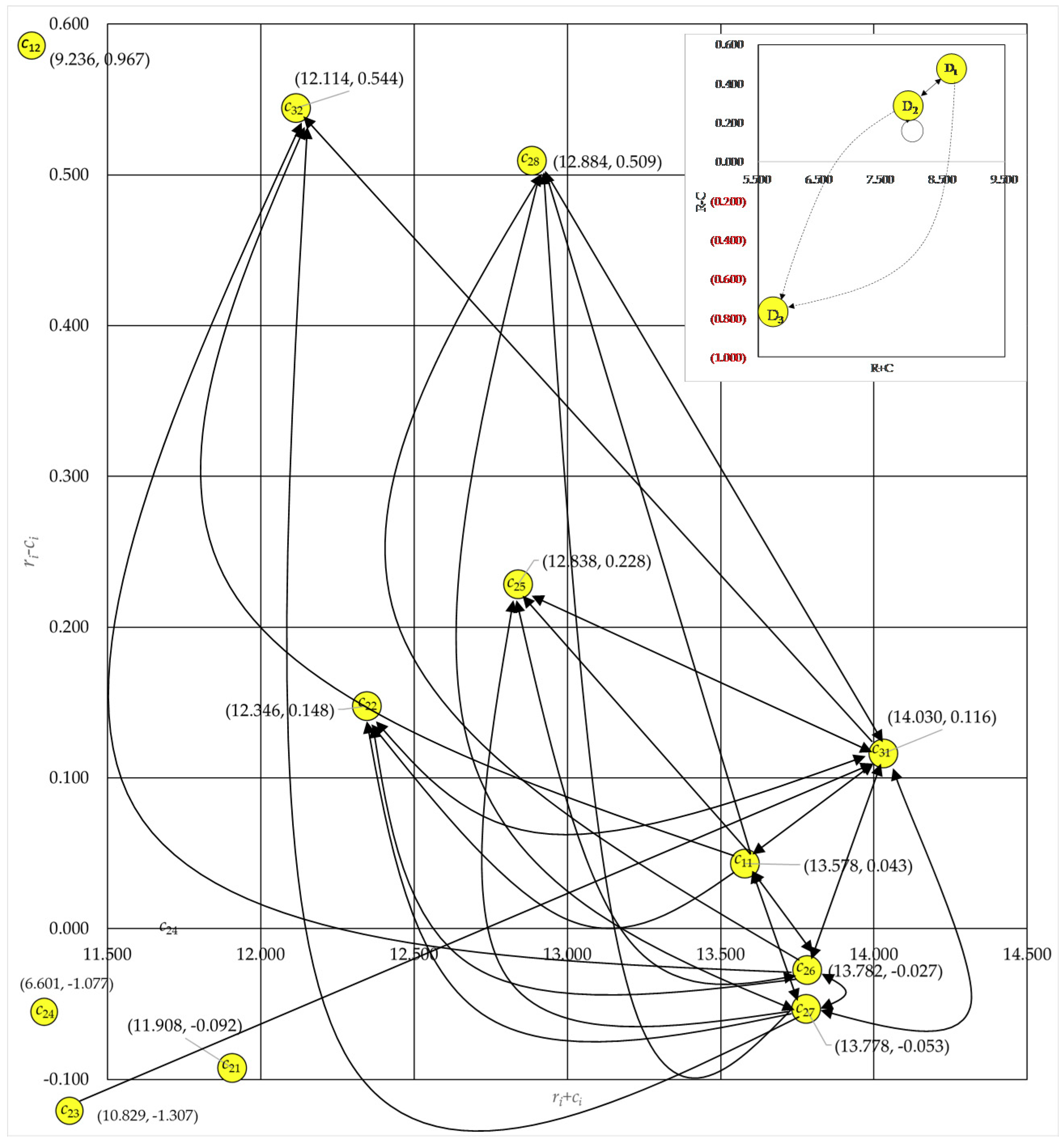
According to the analytical results (Table 9) derived by the DNP, the process and geometric attributes (D2) were ranked as the most important dimension. The influence weighs 0.648. The other two dimensions were less important than the process and geometric attributes. Meanwhile, based on the IRM of dimensions demonstrated in the upper right of Figure 2, the material dimension (D1) and the process and geometric dimension (D2) influence each other. The two dimensions influence the economic dimension (D3). This finding is consistent with earlier works. Tadigadapa and Najafi [115] argued that at the MEMS scale, at which the thickness of materials is typically a few microns, changes in fabrication processes (D2) significantly influence their material (D1) and mechanical properties. According to Gaura and Newman [116], it is a must to carefully concurrently ponder over the materials (D1) employed in the fabrication of a particular device and the process flow (D2), and this coherent planning will form part of the material selection process. It is not rare to find that the ‘best’ material to use based on the quantitative material selection often turns out to be impracticable as a result of processing incompatibility. When faced with such a predicament, a compromise should be ready to come into play as a substitute [116]. As stated by Tadigadapa and Najafi [115], the choice of the fabrication process (D2) is very important in that it defines the overall performance and cost (D3) of the micromachined part. Burger et al. [117] also mentioned that technology development teams in MEMS companies work on new concepts to reduce costs (D3) through miniaturization and a decrease of material consumption (D1) [117,118,119]. Next, the most influential criteria for each dimension will be discussed.
For the first dimension, namely, the Material Attributes (D1), the criterion for evaluating the most suitable material for the PM2.5 sensor fabrication was evaluated and selected. Based on the analytical results, suitability for the main structural material ( c 11 ) is critical from the aspect of material selection and is ranked fourth. The weight associated with the criterion is 9.455%. As the PM2.5 sensor device is directly connected with the substrate, the device material and the structural material for the substrate are closely related. Thus, the fabrication and reliability of the PM2.5 sensor device will be influenced by the main structural material. For the other criteria in this dimension, i.e., suitability for nonstructural purposes ( c 12 ), the importance to the criterion is comparatively lower, 7.089%, and it is ranked 10th. Applications of materials for nonstructural purposes usually include processes such as metallization and insulation layers [48]. According to Bali [53], metallization is the final step in the wafer-processing sequence, and aims to connect the individual devices to form an integrated circuit. As defined by Jones [54], an insulator is a material that blocks the flow of electric current. As the metallization layer aims to provide connections between devices, and the insulation layer aims to block currents inside the sensor device, the materials are generally independent of the bulk material. That is, no matter which material is selected (e.g., Si, GaAs, or GaN), these metallization and insulation layers are still used. Therefore, independence between the suitability for the main structural material ( c 11 ) and the suitability for nonstructural purposes ( c 12 ) is reasonable.
For the second dimension, namely, the Process and Geometric Attributes (D2), technology readiness ( c 26 ) and yield ( c 27 ) are the most influential criteria. Based on the analytical results, technology readiness ( c 26 ) and yield ( c 27 ) are critical for the PM2.5 MEMS process and are ranked second and third, respectively. The weights associated with the criteria are 9.556% and 9.542%, respectively. While evaluating the technology readiness ( c 26 ) of a novel sensor technology, the key decision factor is whether the material can be fabricated using the widely adopted low-cost photolithography and etching equipment. Therefore, the technology’s readiness ( c 26 ) was assigned a rank of second place (see Table 10). Whether the device can be successfully commercialized or is technology-ready ( c 26 ) will further be determined based on three factors: (1) whether the characteristics of the PM2.5 sensors fabricated in the initial stage of the product life cycle are compatible with product specifications; (2) whether the yield ( c 27 ) will be sufficiently high to achieve economy of scale; and (3) whether the reliability ( c 28 ) of the sensor meets the requirement of the specification when the sensor is applied under various environments over the long term. The above characteristics for evaluating technology readiness are compatible with the influence relationships demonstrated.
The yield ( c 27 ) is of course one of the most important factors in evaluating and selecting the materials. Based on the yield of the PM2.5 sensor, a decision can be made as to whether the materials ( c 11 ) should be adjusted. Meanwhile, based on the device structure being finished, whether the precision ( c 25 ) of the photolithography alignment is influenced can be further analyzed. Whether the process design can be changed so as to enhance the yield should be considered. If the yield ( c 27 ) cannot be improved, then better equipment to enhance the precision ( c 25 ) of the photolithography alignment should be adopted.
Good yield ( c 27 ) does not imply high reliability ( c 28 ). Reliability depends not only on the characteristics of the device, but also on its operating environment. If a poor operating environment can damage the PM2.5 sensors, then we must consider changing the structure and material of the device to achieve better reliability. Therefore, the yield and reliability are closely interrelated, and neither one can be considered independently. Hence, in the inchoate stages of the product life cycle, before the new PM2.5 sensor products have been commercialized, these two criteria need to be carefully considered and evaluated.
In the third dimension (D3), the capability of the sensor to be mass-produced ( c 31 ) will influence future investments ( c 32 ). Based on the analytical results, the capability of the sensor to be mass-produced ( c 31 ) is critical from the economic aspect and is ranked first in this research. The weight associated with the criterion is 9.814%. When the technology has reached the mass production stage of the product life cycle, investments in the equipment required for mass production are essential. Equipment, manpower, and thus mass production capacity will be greatly improved. When a new sensor product technology has been proven to be mature and stable after the pilot run of product testing, the mass production process can be initiated. Numerous problems can arise at the mass production stage. Such problems should be overcome although problems will keep emerging. The initiation of mass production may be delayed. Investments in automatic production and measuring equipment and related production analysis management tools can facilitate mass production. Hence, the mass production capability and thus competitive advantages can be improved.

5.3. Mutual Influences between the Most Important Criteria

The mutual influences between the suitability of the main structural material ( c 11 ), technology readiness ( c 26 ), yield ( c 27 ), and capability to be mass-produced ( c 31 ) are interesting and worthy of further discussion. As introduced in Section 5.1, MEMS wafers need to be made from as high quality a material as possible; yet, they should be inexpensive to manufacture [105]. Meanwhile, according to Uttamchandani [120], high yield ( c 27 ) of MEMS structures comes from a highly stable and firmly reproducible fabrication process, which is formidable and hard to realize in real-world implementations, and consequently, has remained a grave challenge as well as one of the bottlenecks in MEMS commercialization ( c 31 ) [120]. Furthermore, according to the definitions of technology readiness levels (TRLs) ( c 26 ), the highest level of technology readiness, or the TRL9, can be defined as an actual system proven through successful mission operations [121]. Based on the report of the Next-generation Low-Cost Multifunctional Web Enabled Ocean Sensor Systems (NeXOS) project [122], granted by the European Commission, TRL 9 means full commercial application, or that the technology is available for the consumer. Apparently, yield ( c 27 ) can influence the MEMS commercialization capabilities ( c 31 ) and thus, the technology readiness level ( c 26 ).
According to Quinn et al. [48], the value of MEMS devices often depends on whether or not their mass production is achieved ( c 31 ). If the MEMS devices have already reached their mass production stage, large capital investments ( c 32 ) can be paid off over time. The influence relation is consistent with recent works. According to Jiang et al. [111], the GaN can be produced on a large scale with a mature preparation process. The work by Jiang et al. [111] is consistent with a recent report mentioning the significant capital and engineering investment in GaN manufacturing capability by TSMC, the industry leader of semiconductor foundries [123].
As mentioned in Section 5.2, once the technology has reached the mass production stage ( c 31 ) of the product life cycle, investments in the equipment required for mass production are essential. Equipment, manpower, and thus mass production capacity will be greatly improved. This is consistent with the work by Bhala [124], mentioning that businesses prefer not to invest in physical capital equipment for a new product until its features are settled, the exact market identified, and the best way to automate production determined. When a new sensor product technology has been proven to be mature and stable after the pilot run of product testing, the mass production process can be initiated. Numerous problems can arise in the mass production stage. Investments in automatic production, measuring equipment, and related production analysis management tools can resolve these problems, and thus increase the yield ( c 27 ), technology readiness ( c 26 ), and facilitate production ( c 31 ).
Based on the same rationale, the capability to be mass-produced ( c 31 ) can influence the investment in automatic production, measuring equipment, and related production analysis management tools. Thus, the precision of the MEMS, and thus reliability in terms of the consistency of the MEMS sensor with the specification, can be enhanced. Thus, precision ( c 25 ) and reliability ( c 28 ) can be influenced directly by the capability to be mass-produced ( c 31 ). The capability to be mass-produced ( c 31 ) can further influence precision ( c 25 ) and reliability ( c 28 ) through the material, yield ( c 27 ), and technology readiness ( c 26 ). This finding is consistent with the argument by Burkacky et al. [125] and the yield-learning procedure mentioned by Weber [126]. Recently, Burkacky et al. [125] found that the problems do not stop after chips enter the market ( c 31 ): customers may encounter unexpected performance issues ( c 25 and c 28 ) and ask semiconductor companies to help resolve them. In many cases, problems arise because important tasks still require frequent manual intervention, despite having some degree of automation. To improve the process, many technology companies are now creating analytical tools that could help fabs replace guesswork and human intuition with fact-based knowledge, pattern recognition, and structured learning [125]. According to Weber [126], in order to achieve yields ( c 27 ) near 100%, i.e., technology readiness ( c 26 ), a semiconductor manufacturer needs to master a procedure called yield learning, which essentially consists of eliminating one source of faults ( c 25 ) after another until an overwhelming portion of manufactured units function according to specification ( c 31 ). By using advanced data analytics, companies can correct errors in physical designs and improve yield ( c 27 ) and reliability ( c 28 ) without running a single wafer or making a mask [125].

5.4. The Independent Criteria

Another criteria belonging to the dimension, the suitability for nonstructural purposes ( c 12 ), has comparatively lower importance (7.089%), and ranked in 10th place. The applications of materials for nonstructural purposes usually include processes such as metallization or insulation layers [48]. According to Bali [53], metallization is the final step in the wafer-processing sequence which aims to connect the individual devices in an integrated circuit. As defined by Jones [54], an insulator is a material that blocks the flow of electric current. As the metallization layer provides connections between devices and the insulation layer aims to block currents inside the sensor device, the materials are generally independent from the bulk material. That is, no matter which material(s) from the Si, GaAs, or GaN is selected, these metallization or insulation layers are still used. Therefore, the independence between the suitability for main structural material ( c 11 ) and the suitability for nonstructural purposes ( c 12 ) is reasonable.
The surface attribute includes the in-plane surface roughness of the beam as well as its out-of-plane/wall roughness [48]. For the design of mirrors and the reduction of stiction, the roughness is of particular importance [48]. Besides, the Minimum achievable beam height ( c 24 ) dimensions play an essential role to help ascertain the compactness, natural frequency, and thermal time constants of the devices. These dimensions also assist in finding the sensitivity limits of the sensors and actuators [48]. Although the minimum achievable beam height ( c 24 ) dimensions possess such advantages, they are not applicable in PM2.5 sensor designs. The form factors of PM2.5 sensors are not critical. Meanwhile, the operating frequency is usually only highly critical for communications devices, and is not critical for sensors. Most of the time, PM2.5 sensors operate at ordinary temperatures. Thus, the independence of the surface attribute ( c 12 ) from other criteria is reasonable.

5.5. Contributions, Limitations, and Future Recommendations

PM2.5 is recognized as one of the most important air pollution issues. Meanwhile, the demand for PM2.5 sensors is surging rapidly in recent years. Most of the newly developed PM2.5 sensors are designed and fabricated by using the MEMS. Selecting an appropriate material for manufacturing an MEMS device or component in general, and for PM2.5 sensors in particular, by considering the material, process, geometric as well as the economic attributes at the same time is not easy. However, very few or no works have tried to investigate what the most appropriate MEMS material is for designing and fabricating future PM2.5 sensors. The evaluation and selection of an MEMS material is, by nature, an MCDM problem. In this work, a HMCDM framework was proposed. Further, the derived influence relationships have been proven to be consistent with prior works. Therefore, we have not only demonstrated the feasibility of the proposed analytic framework but also selected the most suitable MEMS material, GaN, for PM2.5 sensors. The analytic framework and results selected by experts from industry, academic and research institutes are very reasonable and suitable for future applications. In this subsection, we would like to discuss the major contributions, limitations, as well as future recommendations.

5.5.1. Contributions

Firstly, the major contributions will be discussed from three aspects: (1) MEMS material selection; (2) successful integration of TA concepts with MCDM models and successful verification of the models; and (3) the research in sustainability, especially the most up-to-date PM2.5 issue.
From the aspect of MEMS materials selection in general, and the evaluation and selection of MEMS materials for PM2.5 gas sensors in particular, though Za and Du [51] proposed the concept of evaluating and selecting the manufacturing process and material concurrently, based on the authors’ knowledge and experience of the subject, very limited or no prior works model the concurrent evaluation and selection of MEMS materials. Thus, development and verification of the MCDM-based concurrent evaluation and selection of the MEMS materials will be one of the major research contributions.
The successful integration of TA and advanced MCDM models and the successful verification of models by engineering research results also contribute to the management of technology research and decision analysis. Although the concept of TA emerged in the 1960s [11], only recently have scholars started to introduce the concept of influence relations between criteria as well as feedbacks. However, very few works have focused on engineering practices, not to mention verification of the influence relationships and analytic results by using engineering analysis results. This study fully verifies the influence relationships between aspects and criteria as well as the alternatives (GaN) selected by engineering research results in this Section. The comparison results are summarized in Table 12. Such verifications demonstrate the feasibility of the DNP-based HMCDM models based on experts’ opinions.
The selected alternative is consistent with recently published academic works. Rais-Zadeh et al. [109] argued that GaN-based MEMS is becoming popular. In comparison with other alternatives, such as Si and GaAs, in this work, the comparison results are consistent with the most up-to-date research works. According to Lidow [127], for the first time in 60 years, a new higher-performance technology is less expensive to produce than its silicon counterpart. According to Tsao et al. [128], GaN-based transistors had a significant power advantage over GaAs-based transistors; led by GaN-on-Silicon, it is competing to be the next viable alternative to silicon, even as silicon itself continues to evolve towards higher performance (with advances in superjunction MOSFETs, IGBTs, and other devices). Thus, beginning in the 2000s and accelerating in the 2010s, U.S. government investment in GaN electronics research increased within the Department of Defense, especially by DARPA [128]. Nowadays, the GaN can be produced on a large scale with a mature preparation process [111]. Meanwhile, according to Reddeppa et al. [113], GaN provides a new approach to improve the performance of gas sensors in terms of the operating temperature and response time [113]. Apparently, the GaN will be one of the most suitable materials for future MEMS design.
For the influence relationships between the analytic results and engineering research results, we also verified the consistency between the analytic results derived by the HMCDM methods and those derived by engineering research and published in well-known journals (refer to Table 12). Based on the authors’ knowledge and experiences, the results derived by MCDM-based analytic models were seldom verified by engineering research results. The consistency between the results derived by both methods further demonstrates the feasibility and the trustworthiness of the expert-opinion based MCDM models.
In terms of the contributions of this research to sustainability, PM2.5 is apparently a very significant problem which is now threatening the sustainable development of human beings. The successful selection of MEMS materials can enable vendors to provide low-cost and high-precision sensors and thus, accelerate the diffusion of PM2.5 gas sensors. The wide distribution of PM2.5 gas sensors, or even connecting these sensors to the Internet and disclosing this air pollution information, can further enhance public awareness and involvement in environmental sustainability [129]. These sensor technologies enable the capture of environmental data by involving public authorities and the general public, and by making real-time information on environmental conditions available to the wider public [129].

5.5.2. Limitations

In terms of limitations, in this research, the experts were invited to help determine the aspects, criteria, influence relationships, and the influence weights. Unfortunately, the number of qualified experts is very limited in Taiwan due to the limited number of PM2.5 IC vendors. Therefore, the experts are mainly from research and academic institutes, and the results may seem controversial. To provide results with a wider possibility of interpretation, future research may include studies based on the opinions from foreign institutes and firms.

5.5.3. Future Research Possibilities

In terms of future research possibilities, in the past, the silicon substrate was regarded as the most suitable material for sensor technology; however, by considering the daily complicated operation conditions for future PM2.5 sensors (e.g., smart factories, unmanned aerial vehicles, and unmanned cars), which will operate at higher temperatures, a GaN-on-silicon substrate should be considered. GaN-on-silicon means implementing one epitaxial layer of GaN on the silicon substrate. Such a GaN-on-silicon substrate can be fabricated on 8-inch wafers. The PM2.5 sensors fabricated by GaN substrates can operate at high temperature, whereas the PM2.5 sensors fabricated by other materials cannot fulfill this condition. The environmental impacts on the PM2.5 sensors by GaN will be less. The fabrication cost of the GaN-on-silicon substrate will keep reducing, because various sensor materials can be introduced. Thus, PM 2.5 sensors can also be integrated with other gas sensors that detect such species as carbon monoxide (CO), organic solvents, and sulfides. The functionalities and thus utilities of such integrated sensors can be greatly improved, and thereby also the product values. For system designers, such sensor products can be better leveraged.
Furthermore, because the MCDM methods and HMCDM-based approaches have developed rapidly in recent years, recently developed MCDM methods, such as complex proportional assessment (COPRAS), fuzzy additive ratio assessment method (ARAS-F), multi-objective optimization on the basis of ratio analysis (MOORA), multiple objective optimization on the basis of ratio analysis plus full multiplicative form (MULTIMOORA), step-wise weight assessment ratio analysis (SWARA), and weighted aggregated sum product assessment (WASPAS) [131], a combination of the dominance-based rough set approach (DRSA) decision-rules with formal concept analysis (FCA) based DANP [132], etc., can be applied in the future to evaluate suitable materials for sensors or other products in general, and materials for PM gas sensors in particular.

6. Concluding Remarks

PM2.5 is already a possible indicator for the sustainability of human life. Therefore, PM2.5 gas sensors are being developed to help detect air pollution problems in real-time. The evaluation and selection of a suitable MEMS material for fabricating such PM2.5 sensors has become the current focus of firms engaged in new product development as well as the semiconductor foundries aiming to provide wafer fabrication services for PM2.5 sensor providers. In this research, an analytic framework consisting of the DEMATEL, the DNP, as well as the VIKOR was proposed. Possible aspects and criteria that were derived based on the results of the literature review were summarized by the modified Delphi method based on thirteen MEMS experts mainly from Taiwanese research institutes, universities, and semiconductor foundries. Then, the structure of the decision-making problem was configured by using the DEMATEL based on the opinions of experts. The aspects and criteria were then prioritized by using the DNP. The compromise ranking of the MEMS materials for PM2.5 sensors, which include the Si, GaAs, and GaN, was derived by VIKOR.
Based on the empirical results, the important criteria include the mass-production capability, suitability for serving as the main structural material, the choice of material, precision, technology readiness, yield, and reliability. The GaN was selected as the most appropriate MEMS material for fabricating PM2.5 gas sensors. The well-verified analytic framework could be used to select the most suitable materials for PM2.5 sensors as well as for other sensors. Fabless design houses, MEMS foundries, and research institutes could define the technology roadmaps and new product development plans accordingly. Governments could also encourage research projects for PM2.5 sensors and the PM2.5 sensor-based air quality monitors through direct support of firms’ R&D and innovation as well as grants to leading research universities and institutes for advanced study. Furthermore, the wide adoption of PM2.5 sensor-based low-cost monitors by governments could improve environmental monitoring and thus, help protect local air quality and avoid pollution. In the future, other MCDM methods could be introduced into the material selection problems. Comparisons of the analytic research results may provide further insights, from the aspects of decision science, TA, material engineering, and sustainability. Since PM2.5 gas sensors are standalone devices, the applicability of the well-verified analytic framework on complex systems (e.g., the systems-on-chip) also represents an area of future research.

Author Contributions

Conceptualization, C.-Y.H., P.-H.C. and J.Z.S.; Investigation, C.-Y.H.; Methodology, C.-Y.H.; Project administration, C.-Y.H.; Validation, C.-H.W.; Writing—original draft, C.-Y.H. and P.-H.C.; Writing—review & editing, C.-Y.H., Yao-Hua Ho, C.-H.W., M.-C.L. and M.-J.W.

Funding

This article was subsidized by the National Taiwan Normal University (NTNU), Taiwan, ROC.

Conflicts of Interest

The authors declare no conflict of interest.

Appendix A. DEMATEL

The basic DEMATEL formulas, by Tzeng and Huang [99] and Yang et al. [67], are explained in the following five steps.
Step 1: Form the initial direct-relation matrix
For each arbitrary pair of criteria among all the criteria being evaluated, experts are requested to choose one of the five levels that best represents the level of impact that one criterion has over another. For example, when measuring the influence of factor i on factor j, denoted as a i j , experts will assign a value to it and put it in the i th row and the j th column in the initial direct-relation matrix. Hence, if there are n criteria being evaluated in total, an n-by-n initial direct-relation matrix can be formed at the end of experts’ evaluation process. The initial direct-relation matrix A is defined in Equation (A1), where a i j is the degree of influence that the i th objective has on the j th objective.
A = [ a 11 a 1 j a 1 n a i 1 a i j a i n a n 1 a n j a n n ]  
Step 2: Normalize the direct-relation matrix
To guarantee the convergence of matrix multiplication that will be performed in step 3, the direct-relation matrix obtained in step 1 needs to be first normalized through Equation (A2).
N = y A   ,   y = min { 1 / max i j = 1 n a i j , 1 / max j i = 1 n a i j } , i , j { 1 , 2 , , n } .  
Step 3: Calculate the total relation matrix T.
The total-relation matrix T is calculated by summing up the normalized direct-relation matrix obtained in step 2, its square, cube, and all other higher orders when the highest order approaches infinity. If the normalization is done properly in step 2, the addition of matrices will converge to the result dictated by Equation (A3):
T = N + N 2 + N 3 + + N ε = N ( I + N + N 2 + + N ε 1 ) ( I N ) ( I N ) 1 = N ( I N ε ) ( I N ) 1 = N ( I N ) 1 ,   when   ε ,   N ε = [ 0 ] n x   n  
where ε → ∞, I is the identity matrix.
Step 4: Derive the influence strength of the factors
By summing up the values of each row and column of the total relation matrix T obtained in step 3, we can have r values and c values as depicted in Equations (A4) and (A5). The r value (take r i for example) represents the sum of the influences that factor i has on all factors. The c value (take c j for example) represents the sum of the influences that all factors have on the j th factor.
Τ = [ t i j ] , i , j { 1 , 2 , n }  
r = [ r i ] n x 1 = ( j = 1 n t i j ) n x 1  
c = [ c j ] n x 1 = ( i = 1 n t i j ) 1 x n  
Step 5: Construct the causal diagram
A causal diagram can be constructed by using the r values and c values obtained in step 4. More specifically, it is constructed by using the (r + c) values as the x-axis values and by using the (rc) values as the y-axis values. In fact, the value of r i + c i represents the summation of strengths that factor i gives and receives. A higher value of r i + c i means that factor i is more prone to affect and/or be affected by other factors. On the contrary, the value of r i c i helps discern whether factor i acts more like a dominator (a factor that has great influence over other factors) or an acceptor (a factor that is good at being influenced by other factors). In other words, if r i c i is positive, factor i is good at influencing and thus can be seen as a “cause factor”. If r i c i is negative, factor i is good at being influenced and thus can be regarded as an “effect factor” [84].
Step 6: Set a threshold value and obtain the Network Relation Map (NRM)
If the total-relation matrix T in step 3 contains too much trivial information to comprehend the whole picture accurately, it is wise and necessary to set a threshold value α to filter out minor or irrelevant relationships between factors. That is to say, if a value in matrix T is higher than the threshold value, it stays in the matrix. On the other hand, if a value in matrix T is lower than the threshold value, it will be replaced with zero. The threshold value can come from the consensus of the experts. After the threshold value is decided and the filtering is executed, step 5 can be performed again and the NRM can be drawn accordingly.

Appendix B. Analytic Network Process (ANP)

The following are explanations of the ANP formulas based on Saaty [93] and Yang et al. [132].
Step 7: Construct an unweighted supermatrix based on pairwise comparison matrices of elements.
The original supermatrix W of column eigenvectors can be derived from pairwise comparison matrices of elements (refer Equation (A6)). C n denotes the n th cluster and e n m denotes the m th criterion in the n th cluster. W i j (refer to Equation (A7)) in the supermatrix W is a principal eigenvector of the influence of the elements in the ith component of the network on an element in the j th component. Moreover, if the jth cluster has no influence on the ith cluster, then W i j = [ 0 ] .
W = C 1 C 2 C m e 11 e 1 n 1 e 21 e 2 n 2 e m 1 e m n m e 11 e 12 C 1 e 1 n 1 e 21 e 22 C 2 e 2 n 2 e m 1 e m 2 C m e m n m [ W 11 W 12 W 1 m W 21 W 22 W 2 m W m 1 W m 2 W m m ]
W i j = [ w i 1 j 1 w i 1 j 2 w i 1 j n j w i 2 j 1 w i 2 j 2 w i 2 j n w i n i j 1 w i n i j 2 w i n i j n j ]  
Step 8: Derive the weighted supermatrix by multiplying the normalized matrix.
After forming the supermatrix, the weighted supermatrix can be derived by transforming the sum of all columns to unity exactly. The weighted supermatrix is raised to limiting powers, such as Equation (A8) to obtain the global priority vector or called weights.
lim θ W θ  
Moreover, if the supermatrix has the effect of cyclicity, the limiting supermatrix is not the only one. There are two or more limiting supermatrices in this situation. Thus, the Cesaro sum, formulated by using the following Equation (A9), will be required to derive the weights versus each criterion.
lim ψ ( 1 ν ) j = 1 ν W j ψ  
The average of the limiting supermatrix will be used to calculate the average priority weights, where Wj denotes the jth limiting supermatrix.

Appendix C. The DNP

Based on the total relation matrix T being derived in Appendix A, the influence weights versus each criterion can be derived by using the DNP introduced in this Section. According to Saaty and Vargas [133], the influence of elements in the network on other elements in that network can be represented in the supermatrix. Each column of W i j is a principal eigenvector of the influence (or importance) of the elements in the ith column of the network on an element in the jth row. Since any element t i j in the total-influence matrix T derived by DEMATEL denotes the influence of a factor in the ith row on a factor in the jth column, the total-influence matrix is transposed to fit into the definition of the supermatrix defined in Equation (A6). Let T C be equal to the transposed matrix of the total-influence matrix T = [ t i j ] n x n , i.e., T C = T t . The total relationship matrix can be divided into submatrices according to the criterion belonging to the aspects. The submatrices can be denoted as T c i j = [ t i μ j ν ] , where 1 i μ i n i and 1 j v i n j . Here, n i and n j are the numbers of criteria which belong to the ith dimension, D i , and the j th dimension, D j , respectively.
T c = D 1 D j D m D 1 D i D m [ T c 11 T c 1 j T c 1 m T c i 1 T c i j T c i m T c m 1 T c m j T c m m ] ,
where
T c i j = [ t i 1 j 1 t i 1 j ν t i 1 j n j t i μ j 1 t i μ j ν t i μ j n j t i n i j 1 t i n i j ν t i n i j n j ] .  
Each column of Equation (A11) can be further normalized by using the following Equation (A12):
d j n j = i = i 1 i n i t i n i j n j , j n j = 1 , , i n i .  
Then, the total-influence matrix can be normalized by using the following Equation (A13):
T c i j ( N ) = [ t i 1 j 1 d j 1 t i 1 j ν d j v t i 1 j n j d j n j t i μ j 1 d j 1 t i u j ν d j ν t i μ j n j d j n j t i n i j 1 d j 1 t i n i j ν d j ν t i n i j n j d j n j ] .  
Step 9:
The normalized total-influence matrix, T c ( N ) , can serve as the unweighted supermatrix W as defined in Equation (A6). To derive the weighted super matrix, the values of the elements belonging to each submatrix, T c i j , belonging to the matrix T C , can be added up and filled into a matrix T D as the following Equation (14):
T D = D 1 D j D m D 1 D i D m [ t c 11 t c 1 j t c 1 m t c i 1 t c i j t c i m t c m 1 t c m j t c m m ] ,
where t c i j is the sum of all the elements belonging to the submatrix T c i j . Then, the matrix T D can be normalized by normalizing each column to unity as follows, where d j = i = 1 m t c i j .
T D ( N ) = D 1 D j     D m D 1 D i D m [ t c 11 d 1 t c 1 j d j t c 1 m d m t c i 1 d 1 t c i j d j t c i m d m t c m 1 d 1 t c m j d j t c m m d m ] ,
Step 10:
The weighted supermatrix Π can be derived by multiplying the transposed T D ( N ) with W , i.e., Π = T D ( N ) t W . Then, Equation (A8) can be introduced to derive the weighted supermatrix as follows.
lim θ Π θ .  
The global priority vectors can be derived accordingly.

Appendix D. The VIKOR

The VIKOR method aims to derive a compromise solution with the shortest distance to the ideal solution [134]. At first, we denote the alternatives using the notations A 1 , A 2 , , A l , , A m . The performance score of the j t h criterion is denoted by f l j for alternative A l . The weight versus the j t h criterion is denoted by w j , where j = 1 , 2 , , n . n is the number of criteria. The VIKOR process is initiated by deriving the L p -metric at first:
L l p = { j = 1 n [ w j ( | f j * f l j | ) / ( | f j * f j | ) ] p } 1 / p  
where 1 p ; l = 1 , 2 , , m ; the weight versus the j t h criterion, w j can be derived by using the DNP method which has already been introduced in the former Appendix C. The L l p = 1 (as S l ) and L l p = (as Q l ) are also introduced to formulate the measures for ranking as follows [101,135]:
S l = L l p = 1 = j = 1 n [ w j ( | f j * f l j | ) / ( | f j * f j | ) ] ,
Q l = L l p = = max j { w j ( | f j * f l j | ) / ( | f j * f j | ) | j = 1 , 2 , , n }  
The min l L l p will be selected as the compromise solution due to the minimum value or closest distance to the aspiration level. Furthermore, when p is small, the group utility is emphasized (such as p = 1 ). As p approaches infinity (i.e., p ), the individual maximal regrets and gaps obtain higher importance, as shown by Yu [77,135]. Hence, the min l S l emphasizes the maximum group utility while the min l Q l emphasizes choosing the minimum of the maximum individual regrets.
Based on the concepts mentioned above, the ranking algorithm of VIKOR can be defined as follows.
Step 11:
Normalize the original rating matrix. The aspiration level of some specific function f , i.e., f j * = max l f l j , and the minimum tolerable level of the function, i.e., f j = min l f l j , can be determined. Here, f j * and f j are the best and worst values of all criteria, respectively; j = 1 , 2 , , n . can be determined in this step. Furthermore, the original rating matrix is normalized as a weight-rating matrix by using the following equation.
r l j = ( | f j * f l j | ) / ( | f j * f j | ) .
Step 12:
Derive the mean of the group utility and the maximal regret. The mean of the group utility S l , and the maximal regret, Q l , can be derived by using S l = j = 1 n w j r l j and Q l = max j { r l j | j = 1 , 2 , , n } , where l = 1 , 2 , , m . Traditionally, Q l was formulated as max j { w j r l j | j = 1 , 2 , , n } . That is, the importance of the group utility is higher than the maximal regret. However, in the real cases, the maximal regret is always regarded as critical and is always considered as an aspect to be improved. Hence, to balance the importance of both S l and Q l ,
Q l = max j { r l j | j = 1 , 2 , , n }  
is introduced instead of the traditional VIKOR Q l .
Step 13:
Derive the index values. The index values, R l , l = 1 , 2 , , m , can be formulated as R l = v ( S l S * ) / ( S S * ) + ( 1 v ) ( Q l Q * ) / ( Q Q * ) , where S * = min l S l , S = max l S l , Q * = min l Q l , and Q = max l Q l . Here, the best value can also be defined as 0 while the worst value can be defined as 1. The weight versus the alternative of the maximum group utility can be denoted as v, where 0 v 1 . The weight versus the alternative of the individual regret can be defined as 1 v accordingly.
Step 14:
Rank the alternatives. The alternatives can be ranked by sorting the value of S l and Q l as well as R l , in decreasing order, where l = 1 , 2 , , m . An alternative can be proposed as a compromise solution if both the advantage and stability conditions can be fulfilled. Based on this principle, the alternative ( A ( 1 ) ) can be proposed as a compromise solution which is the best ranked by the measure min { R l | l = 1 , 2 , , m } in the case that the two criteria can be fulfilled: C 1 . Acceptable advantage: R ( A ( 2 ) ) R ( A ( 1 ) ) D R , where the alternative A ( 2 ) is ranked second based on the value of R and m is the number of alternatives while D R = 1 / ( m 1 ) . C 2 Acceptable stability in decision making: A ( 1 ) must be ranked as the best alternative based on S l and/or Q l , where l = 1 , 2 , , m . Further, in the case that any one of the following criteria cannot be fulfilled, a set of compromise solutions will be proposed: (1) The set consists of both A ( 1 ) and A ( 2 ) in the case that the first condition C 1 is fulfilled, whereas the second condition C 2 cannot be fulfilled. (2) The set consists of M alternatives, A ( 1 ) , A ( 2 ) , , A ( M ) , in the case that the first condition C 1 cannot be satisfied. A ( M ) can be determined by R ( A ( M ) ) R ( A ( 1 ) ) < D R , for the maximum M , where the positions of these alternatives are close.

References

  1. Public Health England. What is Particulate Matter? Available online: https://observatory.derbyshire.gov.uk/IAS/Custom/resources/HealthandWellbeing/Health_Protection/PHE_Particulate_matter.pdf (accessed on 24 August 2018).
  2. Galvez, M.P.; Peters, R.; Graber, N.; Forman, J. Effective Risk Communication in Children’s Environmental Health: Lessons Learned from 9/11. Pediatr. Clin. N. Am. 2007, 54, 33–46. [Google Scholar] [CrossRef] [PubMed]
  3. Zhang, R.; Jing, J.; Tao, J.; Hsu, S.-C.; Wang, G.; Cao, J.; Lee, C.S.L.; Zhu, L.; Chen, Z.; Zhao, Y. Chemical characterization and source apportionment of PM 2.5 in Beijing: Seasonal perspective. Atmos. Chem. Phys. 2013, 13, 7053–7074. [Google Scholar] [CrossRef]
  4. World Health Organization. World Health Organization Issues Recommendations to Tackle Health Impacts of Air Pollution in Mongolia. Available online: http://www.wpro.who.int/mongolia/mediacentre/releases/20180228_recommendations_air_pollution/en/ (accessed on 19 August 2018).
  5. World Health Organization. Air Pollution Levels Rising in Many of the World’s Poorest Cities. Available online: http://www.who.int/en/news-room/detail/12-05-2016-air-pollution-levels-rising-in-many-of-the-world-s-poorest-cities (accessed on 19 August 2018).
  6. Barwick, P.J.; Li, S.; Rao, D.; Zahur, N. The Morbidity Cost of Air Pollution: Evidence from Consumer Spending in China; National Bureau of Economic Research: Cambridge, MA, USA, 2018. [Google Scholar]
  7. Yole. Yole’s Analysts Believe in a Wide Adoption of Gas Sensors in Consumer Products. Available online: http://www.yole.fr/Gas_Sensor_ConsumerMarket.aspx#.W3wstugzYrg (accessed on 22 August 2018).
  8. Research and Markets. Environmental Gas Sensors Market 2017–2027. Available online: https://globenewswire.com/news-release/2017/05/11/982339/0/en/Environmental-Gas-Sensors-Market-2017-2027.html (accessed on 22 August 2018).
  9. MarketsandMarkets. Air Quality Monitoring System Market worth 4.90 Billion USD by 2022. Available online: https://www.marketsandmarkets.com/PressReleases/air-quality-monitoring-equipment.asp (accessed on 22 August 2018).
  10. Clements, A.L.; Griswold, W.G.; Rs, A.; Johnston, J.E.; Herting, M.M.; Thorson, J.; Collier-Oxandale, A.; Hannigan, M. Low-cost air quality monitoring tools: From research to practice (a workshop summary). Sensors 2017, 17, 2478. [Google Scholar] [CrossRef] [PubMed]
  11. Locatis, C.N.; Gooler, D.D. Evaluating second-order consequences: Technology assessment and education. Rev. Educ. Res. 1975, 45, 327–353. [Google Scholar] [CrossRef]
  12. Goodman, C.S. Introduction to Health Technology Assessment; The Lewin Group: Falls Church, VA, USA, 2004. [Google Scholar]
  13. Grunwald, A. Technology assessment. In Encyclopedia of Information Science and Technology, 3rd ed.; IGI Global: Hershey, PA, USA, 2015; pp. 3998–4006. [Google Scholar]
  14. Ely, A.; Van Zwanenberg, P.; Stirling, A. Broadening out and opening up technology assessment: Approaches to enhance international development, co-ordination and democratisation. Res. Policy 2014, 43, 505–518. [Google Scholar] [CrossRef] [Green Version]
  15. Berloznik, R.; Van Langenhove, L. Integration of Technology Assessment in R&D Management Practices. Technol. Forecast. Soc. Chang. 1998, 58, 23–33. [Google Scholar]
  16. Coates, J.F. The role of formal models in technology assessment. Technol. Forecast. Soc. Chang. 1976, 9, 139–190. [Google Scholar] [CrossRef]
  17. Smits, R.; Leyten, J. Technology Assessment: Waakhond of Speurhond? Vrije University Press: Kerckebosch, Zeist, The Netherlands, 1991. [Google Scholar]
  18. Van Den Ende, J.; Mulder, K.; Knot, M.; Moors, E.; Vergragt, P. Traditional and modern technology assessment: Toward a toolkit. Technol. Forecast. Soc. Chang. 1998, 58, 5–21. [Google Scholar] [CrossRef]
  19. UN Branch for Science and Technology for Development. United Nations Workshop on Technology Assessment for Developing Countries; UN Branch for Science and Technology for Development: Washington, DC, USA, 1991. [Google Scholar]
  20. European Parliamentary Technology Assessment. What is Technology Assessment? Available online: http://eptanetwork.org/index.php/about/what-is-ta (accessed on 31 March 2018).
  21. Tran, T.A.; Daim, T. A taxonomic review of methods and tools applied in technology assessment. Technol. Forecast. Soc. Chang. 2008, 75, 1396–1405. [Google Scholar] [CrossRef]
  22. Baark, E. Development Technology Assessment—Some Theoretical and Methodological Issues. In Proceedings of the Workshop on Technology Assessment for Developing Countries, Washington, DC, USA, November 1991. [Google Scholar]
  23. Smits, R.; Leyten, J.; Den Hertog, P. Technology assessment and technology policy in Europe: New concepts, new goals, new infrastructures. Policy Sci. 1995, 28, 271–299. [Google Scholar] [CrossRef]
  24. Grin, J.; Van de Graaf, H. Technology assessment as learning. Sci. Technol. Hum. Values 1996, 21, 72–99. [Google Scholar] [CrossRef]
  25. Van Eijndhoven, J.C. Technology assessment: Product or process? Technol. Forecast. Soc. Chang. 1997, 54, 269–286. [Google Scholar] [CrossRef]
  26. Brom, F.; van Est, R. Technology assessment as an analytic and democratic practice. In Encyclopedia of Applied Ethics, 2nd ed.; Elsevier: Amsterdam, The Netherlands, 2011. [Google Scholar]
  27. World Health Organization. Health Technology Assessment. Available online: http://www.who.int/health-technology-assessment/about/Defining/en/ (accessed on 31 March 2017).
  28. Ammenwerth, E.; Rigby, M. Evidence-Based Health Informatics: Promoting Safety and Efficiency Through Scientific Methods and Ethical Policy; IOS Press: Amsterdam, The Netherlands, 2016. [Google Scholar]
  29. Roessner, J.D.; Frey, J. Methodology for technology assessment. Technol. Forecast. Soc. Chang. 1974, 6, 163–169. [Google Scholar] [CrossRef]
  30. Henriksen, A.D.P. A technology assessment primer for management of technology. Int. J. Technol. Manag. 1997, 13, 615–638. [Google Scholar] [CrossRef]
  31. Lendaris, G.G. Structural modeling—A tutorial guide. IEEE Trans. Syst. Man Cybern. 1980, 10, 807–840. [Google Scholar] [CrossRef]
  32. White, H. DFID Economists’ Manual: Impact Evaluation; World Bank: Washington, DC, USA, 2006. [Google Scholar]
  33. Palm, E.; Hansson, S.O. The case for ethical technology assessment (eTA). Technol. Forecast. Soc. Chang. 2006, 73, 543–558. [Google Scholar] [CrossRef]
  34. Swart, R.J.; Raskin, P.; Robinson, J. The problem of the future: Sustainability science and scenario analysis. Glob. Environ. Chang. 2004, 14, 137–146. [Google Scholar] [CrossRef]
  35. Banuls, V.A.; Salmeron, J.L. A scenario-based assessment model—SBAM. Technol. Forecast. Soc. Chang. 2007, 74, 750–762. [Google Scholar] [CrossRef]
  36. Wilhite, A.; Lord, R. Estimating the risk of technology development. Eng. Manag. J. 2006, 18, 3–10. [Google Scholar] [CrossRef]
  37. Ramanujam, V.; Saaty, T.L. Technological choice in the less developed countries: An analytic hierarchy approach. Technol. Forecast. Soc. Chang. 1981, 19, 81–98. [Google Scholar] [CrossRef]
  38. Bohm, E.; Walz, R. Life–cycle–analysis: A methodology to analyse ecological consequences within a Technology Assessment Study? Int. J. Technol. Manag. 1996, 11, 554–565. [Google Scholar]
  39. Fleischer, T.; Decker, M.; Fiedeler, U. Assessing emerging technologies—Methodological challenges and the case of nanotechnologies. Technol. Forecast. Soc. Chang. 2005, 72, 1112–1121. [Google Scholar] [CrossRef]
  40. Tran, T.; Daim, T.U. Technology Assessment. In Technology Assessment: Forecasting Future Adoption of Emerging Technologies; Daim, T., Gerdsri, N., Basoglu, N., Eds.; Erich Schmidt Verlag GmbH & Co.: Berlin, Germany, 2011; Volume 10. [Google Scholar]
  41. Snyder, E.G.; Watkins, T.H.; Solomon, P.A.; Thoma, E.D.; Williams, R.W.; Hagler, G.S.; Shelow, D.; Hindin, D.A.; Kilaru, V.J.; Preuss, P.W. The Changing Paradigm of Air Pollution Monitoring; ACS Publications: Washington, DC, USA, 2013. [Google Scholar]
  42. Hagler, G.; Solomon, P.; Hunt, S. New Technology for Low-Cost, Real-Time Air Monitoring; Air & Waste Management Association: Pittsburg, PA, USA, 2014. [Google Scholar]
  43. Kumar, P.; Morawska, L.; Martani, C.; Biskos, G.; Neophytou, M.; Di Sabatino, S.; Bell, M.; Norford, L.; Britter, R. The rise of low-cost sensing for managing air pollution in cities. Environ. Int. 2015, 75, 199–205. [Google Scholar] [CrossRef] [PubMed] [Green Version]
  44. Geng, H. Internet of Things and Data Analytics Handbook; John Wiley & Sons: Hoboken, NJ, USA, 2017. [Google Scholar]
  45. Spearing, S. Materials issues in microelectromechanical systems (MEMS). Acta Mater. 2000, 48, 179–196. [Google Scholar] [CrossRef]
  46. Leondes, C.T. Mems/Nems: (1) Handbook Techniques and Applications Design Methods, (2) Fabrication Techniques, (3) Manufacturing Methods, (4) Sensors and Actuators, (5) Medical Applications and MOEMS; Springer: New York, NY, USA, 2007. [Google Scholar]
  47. Arzt, E. Size effects in materials due to microstructural and dimensional constraints: A comparative review. Acta Mater. 1998, 46, 5611–5626. [Google Scholar] [CrossRef]
  48. Quinn, D.J.; Spearing, S.M.; Ashby, M.F.; Fleck, N.A. A systematic approach to process selection in MEMS. J. Microelectromec. Syst. 2006, 15, 1039–1050. [Google Scholar] [CrossRef]
  49. Pratap, R.; Arunkumar, A. Material selection for MEMS devices. Indian J. Pure Appl. Phys. 2007, 45, 358–367. [Google Scholar]
  50. Zha, X.F. Manufacturing advisory service system for concurrent and collaborative design of MEMS devices. In MEMS/NEMS; Springer: Berlin, Germany, 2006; pp. 1–34. [Google Scholar]
  51. Zha, X.F.; Du, H. Manufacturing process and material selection in concurrent collaborative design of MEMS devices. J. Micromech. Microeng. 2003, 13, 509. [Google Scholar] [CrossRef]
  52. Pearton, S.J.; Abernathy, C.R.; Ren, F. Gallium Nitride Processing for Electronics, Sensors and Spintronics; Springer: London, UK, 2006. [Google Scholar]
  53. Bali, S.P. Linear Integrated Circuits; Tata McGraw-Hill: New Delhi, India, 2008. [Google Scholar]
  54. Jones, S.W. Introduction to Integrated Circuit Technology, 5th ed.; IC Knowlegde LLC.: Georgetown, MA, USA, 2012. [Google Scholar]
  55. Zhang, Z.; XI, P.; Xiong, L.; Wang, J.; Shi, T. U.S. Patent No. 9,315,379; U.S. Patent and Trademark Office: Washington, DC, USA, 2016. [Google Scholar]
  56. Gao, D.-H.; Qin, M.; Chen, H.-Y.; Huang, Q.-A. A self-packaged thermal flow sensor by CMOS MEMS technology. In Proceedings of the 3rd IEEE international conference on Sensors, Vienna, Austria, 24–27 October 2004; pp. 879–883. [Google Scholar]
  57. All Sensors Corporation. Understanding Accuracy and Precision for MEMS Pressure Sensors. Available online: https://www.allsensors.com/engineering-resources/white-papers/accuracy-and-precision-for-mems-pressure-sensors (accessed on 3 March 2018).
  58. Mankins, J.C. Technology Readiness Levels; Office of Space Access and Technology, NASA: Washington, DC, USA, 1995.
  59. Thornton, A.C. Variation Risk Management: Focusing Quality Improvements in Product Development and Production; John Wiley & Sons, Inc.: Hoboken, NJ, USA, 2004. [Google Scholar]
  60. Mahalik, N.P. MEMS; Tata McGraw-Hill Education: New Dehli, India, 2008. [Google Scholar]
  61. Ou, Y.-C. Using a hybrid decision-making model to evaluate the sustainable development performance of high-tech listed companies. J. Bus. Econ. Manag. 2016, 17, 331–346. [Google Scholar] [CrossRef]
  62. Lu, M.-T.; Tzeng, G.-H.; Cheng, H.; Hsu, C.-C. Exploring mobile banking services for user behavior in intention adoption: Using new hybrid MADM model. Serv. Bus. 2015, 9, 541–565. [Google Scholar] [CrossRef]
  63. Chen, F.-H. Application of a hybrid dynamic MCDM to explore the key factors for the internal control of procurement circulation. Int. J. Prod. Res. 2015, 53, 2951–2969. [Google Scholar] [CrossRef]
  64. Shen, K.-Y.; Tzeng, G.-H. A decision rule-based soft computing model for supporting financial performance improvement of the banking industry. Soft Comput. 2015, 19, 859–874. [Google Scholar] [CrossRef]
  65. Lin, C.-L. A novel hybrid decision-making model for determining product position under consideration of dependence and feedback. Appl. Math. Model. 2015, 39, 2194–2216. [Google Scholar] [CrossRef]
  66. Lin, C.-L.; Shih, Y.-H.; Tzeng, G.-H.; Yu, H.-C. A service selection model for digital music service platforms using a hybrid MCDM approach. Appl. Soft Comput. 2016, 48, 385–403. [Google Scholar] [CrossRef]
  67. Yang, C.-L.; Huang, C.-Y.; Kao, Y.-S.; Tasi, Y.-L. Disaster Recovery Site Evaluations and Selections for Information Systems of Academic Big Data. Eurasia J. Math. Sci. Technol. Educ. 2017, 13, 4553–4589. [Google Scholar] [CrossRef] [Green Version]
  68. Chen, J.-C.; Shyu, J.Z.; Huang, C.-Y. Configuring the Knowledge Diffusion Policy Portfolio of Higher Education Institutes. Eurasia J. Math. Sci. Technol. Educ. 2017, 13, 5685–5734. [Google Scholar] [CrossRef]
  69. Huang, C.-Y.; Kao, Y.-S.; Lu, H.-H.; Wu, M.-J. Curriculum Development for Enhancing the Imagination in the Technology Commercialization Process. Eurasia J. Math. Sci. Technol. Educ. 2017, 13, 6249–6283. [Google Scholar] [CrossRef] [Green Version]
  70. Yang, C.-L.; Shieh, M.-C.; Huang, C.-Y.; Tung, C.-P. A Derivation of Factors Influencing the Successful Integration of Corporate Volunteers into Public Flood Disaster Inquiry and Notification Systems. Sustainability 2018, 10, 1973. [Google Scholar] [CrossRef]
  71. Zavadskas, E.; Antucheviciene, J.; Turskis, Z.; Adeli, H. Hybrid multiple-criteria decision-making methods: A review of applications in engineering. Sci. Iran. Trans. A Civ. Eng. 2016, 23, 1–20. [Google Scholar]
  72. Zavadskas, E.K.; Govindan, K.; Antucheviciene, J.; Turskis, Z. Hybrid multiple criteria decision-making methods: A review of applications for sustainability issues. Econ. Res. 2016, 29, 857–887. [Google Scholar] [CrossRef]
  73. Shen, K.-Y.; Zavadskas, E.K.; Tzeng, G.-H. Updated discussions on ‘Hybrid multiple criteria decision-making methods: A review of applications for sustainability issues’. Econ. Res. 2018, 31, 1437–1452. [Google Scholar] [CrossRef]
  74. Mardani, A.; Zavadskas, E.; Govindan, K.; Amat Senin, A.; Jusoh, A. VIKOR Technique: A Systematic Review of the State of the Art Literature on Methodologies and Applications. Sustainability 2016, 8, 37. [Google Scholar] [CrossRef] [Green Version]
  75. Lu, I.-Y.; Kuo, T.; Lin, T.-S.; Tzeng, G.-H.; Huang, S.-L. Multicriteria Decision Analysis to Develop Effective Sustainable Development Strategies for Enhancing Competitive Advantages: Case of the TFT-LCD Industry in Taiwan. Sustainability 2016, 8, 646. [Google Scholar] [CrossRef]
  76. Kuo, T.; Hsu, C.-W.; Li, J.-Y. Developing a Green Supplier Selection Model by Using the DANP with VIKOR. Sustainability 2015, 7, 1661–1689. [Google Scholar] [CrossRef] [Green Version]
  77. Yu, P.-L. A class of solutions for group decision problems. Manag. Sci. 1973, 19, 936–946. [Google Scholar] [CrossRef]
  78. Zeleny, M.; Cochrane, J.L. Multiple Criteria Decision Making; McGraw-Hill: New York, NY, USA, 1982. [Google Scholar]
  79. Dalkey, N.; Helmer, O. An experimental application of the Delphi method to the use of experts. Manag. Sci. 1963, 9, 458–467. [Google Scholar] [CrossRef]
  80. Murry, J.W.; Hammons, J.O. Delphi: A versatile methodology for conducting qualitative research. Rev. High. Educ 1995, 18, 423–436. [Google Scholar] [CrossRef]
  81. Dalkey, N.C. The Delphi method: An experimental application of group opinion. In Studies in the Quality of Life: Delphi and Decision-Making; Dalkey, N.C., Rourke, D.L., Lewis, R., Snyder, D., Eds.; Lexington Books: Lexington, MA, USA, 1972. [Google Scholar]
  82. Judd, R.C. Forecasting to consensus gathering: Delphi grows up to college needs. Coll. Univ. Bus. 1972, 53, 35–38. [Google Scholar]
  83. Brooks, K.W. Delphi Technique: Expanding applications. North Cent. Assoc. Q. 1979, 54, 377–385. [Google Scholar]
  84. Gabus, A.; Fontela, E. World Problems, an Invitation to Further Thought Within the Framework of DEMATEL; Batelle Geneva Research Center: Geneva, Switzerland, 1972. [Google Scholar]
  85. Hwang, B.-N.; Huang, C.-Y.; Wu, C.-H. A TOE approach to establish a green supply chain adoption decision model in the semiconductor industry. Sustainability 2016, 8, 168. [Google Scholar] [CrossRef]
  86. Hwang, B.-N.; Huang, C.-Y.; Yang, C.-L. Determinants and their causal relationships affecting the adoption of cloud computing in science and technology institutions. Innovation 2016, 18, 164–190. [Google Scholar] [CrossRef]
  87. Zhou, Q.; Huang, W.; Zhang, Y. Identifying critical success factors in emergency management using a fuzzy DEMATEL method. Saf. Sci. 2011, 49, 243–252. [Google Scholar] [CrossRef]
  88. Ou Yang, Y.-P.; Shieh, H.-M.; Tzeng, G.-H. A VIKOR technique based on DEMATEL and ANP for information security risk control assessment. Inf. Sci. 2013, 232, 482–500. [Google Scholar] [CrossRef]
  89. Fan, Z.-P.; Suo, W.-L.; Feng, B. Identifying risk factors of IT outsourcing using interdependent information: An extended DEMATEL method. Expert Syst. Appl. 2012, 39, 3832–3840. [Google Scholar] [CrossRef]
  90. Liao, S.; Wu, M.-J.; Huang, C.-Y.; Kao, Y.-S.; Lee, T.-H. Evaluating and Enhancing Three-Dimensional Printing Service Providers for Rapid Prototyping Using the Dematel Based Network Process and Vikor. Math. Probl. Eng. 2014. [Google Scholar] [CrossRef]
  91. Saaty, T.L. Decision Making with Dependence and Feedback: The Analytic Network Process; RWS Publication: Pittsburgh, PA, USA, 1996. [Google Scholar]
  92. Saaty, T.L. Theory and Applications of the Analytic Network Process—Decision Making with Benefits, Opportunities, Costs, and Risks; RWS Publications: Pittsburg, PA, USA, 2005. [Google Scholar]
  93. Saaty, T.L. Fundamentals of the analytic network process. In Proceedings of the International Symposium on Analytical Hierarchy Process, Kobe, Japan, 12–14 August 1999. [Google Scholar]
  94. Liu, C.-H.; Tzeng, G.-H.; Lee, M.-H. Improving tourism policy implementation—The use of hybrid MCDM models. Tour. Manag. 2012, 33, 413–426. [Google Scholar] [CrossRef]
  95. Phillips-Wren, G.; Jain, L.C.; Nakamatsu, K.; Howlett, R.J. Advances in Intelligent Decision Technologies: Proceedings of the Second Kes International Symposium Idt 2010; Springer: Berlin, Germany, 2010. [Google Scholar]
  96. Huang, C.-Y.; Shyu, J.Z. Developing e-commerce business models for enabling silicon intellectual property transactions. Int. J. Inf. Technol. Manag. 2006, 5, 114–133. [Google Scholar] [CrossRef]
  97. Huang, C.-Y.; Tzeng, G.H.; Ho, W.R. System on Chip Design Service e-Business Value Maximization Through a Novel MCDM Framework. Expert Syst. Appl. 2010, 38, 7947–7962. [Google Scholar] [CrossRef]
  98. Huang, C.-Y.; Shyu, J.Z.; Tzeng, G.H. Reconfiguring the Innovation Policy Portfolios for Taiwan’s SIP Mall Industry. Technovation 2007, 27, 744–765. [Google Scholar] [CrossRef]
  99. Tzeng, G.-H.; Huang, C.-Y. Combined DEMATEL technique with hybrid MCDM methods for creating the aspired intelligent global manufacturing & logistics systems. Ann. Oper. Res. 2012, 197, 159–190. [Google Scholar]
  100. Saaty, T.L. The Analytic Hierarchy Process: Planning, Priority Setting, Resource Allocation; McGraw-Hill: New York, NY, USA, 1980. [Google Scholar]
  101. Opricovic, S. Multicriteria optimization of civil engineering systems. Fac. Civ. Eng. Belgrade 1998, 2, 5–21. [Google Scholar]
  102. Opricovic, S.; Tzeng, G.H. Fuzzy multicriteria model for post earthquake land-use planning. Nat. Hazards Rev. 2003, 4, 59–64. [Google Scholar] [CrossRef]
  103. Hwang, C.-L.; Yoon, K. Multiple Attribute Decision Making; Springer: London, UK, 1981. [Google Scholar]
  104. Yoon, K. A reconciliation among discrete compromise solutions. J. Oper. Res. Soc. 1987, 38, 277–286. [Google Scholar] [CrossRef]
  105. Roy, S.; Sarkar, C.K. MEMS and Nanotechnology for Gas Sensors; CRC Press: Boca Raton, FL, USA, 2015. [Google Scholar]
  106. Jakovenko, J.; Lalinsky, T.; Drzik, M.; Ivanova, M.; Vanko, G.; Husak, M. GaN, GaAs and silicon based micromechanical free standing hot plates for gas sensors. Procedia Chem. 2009, 1, 804–807. [Google Scholar] [CrossRef]
  107. Salehi, A.; Nikfarjam, A. Room temperature carbon monoxide sensor using ITO/n-GaAs Schottky contact. Sens. Actuators B Chem. 2004, 101, 394–400. [Google Scholar] [CrossRef]
  108. Lalinský, T.; Držík, M.; Jakovenko, J.; Vanko, G.; Mozolová, Ž.; Haščík, Š.; Chlpík, J.; Hotový, I.; Řeháček, V.; Kostič, I. GaAs based micromachined thermal converter for gas sensors. Sens. Actuators A Phys. 2008, 142, 147–152. [Google Scholar] [CrossRef]
  109. Rais-Zadeh, M.; Gokhale, V.J.; Ansari, A.; Faucher, M.; Théron, D.; Cordier, Y.; Buchaillot, L. Gallium nitride as an electromechanical material. J. Microelectromec. Syst. 2014, 23, 1252–1270. [Google Scholar] [CrossRef]
  110. Ghodssi, R.; Lin, P. MEMS Materials and Processes Handbook; Springer: New York, NY, USA, 2011. [Google Scholar]
  111. Jiang, Q.-M.; Zhang, M.-R.; Hou, F.; Wang, Z.-G.; Zhang, S.-H.; Chen, Y.; Luo, L.-Q.; Pan, G.-B. In situ bismuth-modified gallium nitride electrode for sensitive determination of cadmium (II) with high repeatability. J. Electroanal. Chem. 2018, 809, 105–110. [Google Scholar] [CrossRef]
  112. Anderson, T.; Ren, F.; Pearton, S.; Kang, B.S.; Wang, H.-T.; Chang, C.-Y.; Lin, J. Advances in hydrogen, carbon dioxide, and hydrocarbon gas sensor technology using GaN and ZnO-based devices. Sensors 2009, 9, 4669–4694. [Google Scholar] [CrossRef] [PubMed]
  113. Reddeppa, M.; Park, B.-G.; Kim, M.-D.; Peta, K.R.; Chinh, N.D.; Kim, D.; Kim, S.-G.; Murali, G. H2, H2S gas sensing properties of rGO/GaN nanorods at room temperature: Effect of UV illumination. Sens Actuators B Chem. 2018, 264, 353–362. [Google Scholar] [CrossRef]
  114. Köck, H.; Chapin, C.A.; Ostermaier, C.; Häberlen, O.; Senesky, D.G. Emerging GaN-based HEMTs for mechanical sensing within harsh environments. In Proceedings of the Sensors for Extreme Harsh Environments, Baltimore, MD, USA, 7–8 May 2014; pp. 9113–9114. [Google Scholar]
  115. Tadigadapa, S.A.; Najafi, N. Developments in microelectromechanical systems (MEMS): A manufacturing perspective. J. Manuf. Sci. Eng. 2003, 125, 816–823. [Google Scholar] [CrossRef]
  116. Gaura, E.; Newman, R. Smart MEMS and Sensor Systems; Imperial College Press: London, UK, 2006. [Google Scholar]
  117. Burger, N.; Staake, T.; Fleisch, E.; Hierold, C. Managing technology development teams–exploring the case of microsytems and nanosystems. R&D Manag. 2013, 43, 162–186. [Google Scholar]
  118. Vigna, B. MEMS epiphany. In Proceedings of the 22nd IEEE International Conference on Micro Electro Mechanical Systems, Sorrento, Italy, 22–25 January 2009; pp. 1–6. [Google Scholar]
  119. Burger, N.; Staake, T. From micro to nanosystems: An exploratory study of influences on innovation teams. Int. J. Soc. Behav. Educ. Econ. Bus. Ind. Eng. 2010, 4, 555–566. [Google Scholar]
  120. Uttamchandani, D. Handbook of Mems for Wireless and Mobile Applications; Woodhead Publishing Limited: Oxford, UK, 2013. [Google Scholar]
  121. Sauser, B.; Verma, D.; Ramirez-Marquez, J.; Gove, R. From TRL to SRL: The concept of systems readiness levels. In Proceedings of the Conference on Systems Engineering Research, Los Angeles, CA, USA, 7–8 April 2006. [Google Scholar]
  122. Dutreuil, S.L.R.; André, X.; Woerther, P.; Quemener, L.; Renaud, C. Technology Readiness Level Report. Available online: http://www.nexosproject.eu/sites/default/files/140422-NXS-WP3_D.3.1-v.final_.pdf (accessed on 10 September 2018).
  123. Semiconductor Today. Navitas Announces TSMC and Amkor Manufacturing Partnerships. Available online: http://www.semiconductor-today.com/news_items/2017/oct/navitas_191017.shtml (accessed on 4 September 2018).
  124. Bhala, R. International Trade Law: Interdisciplinary Theory and Practice; LexisNexis: New York, NY, USA, 2008. [Google Scholar]
  125. Burkacky, O.; Patel, M.; Sergeant, N.; Thomas, C. Reimagining Fabs: Advanced Analytics in Semiconductor Manufacturing. Available online: https://www.mckinsey.com/industries/semiconductors/our-insights/reimagining-fabs-advanced-analytics-in-semiconductor-manufacturing (accessed on 5 September 2018).
  126. Weber, C. Yield learning and the sources of profitability in semiconductor manufacturing and process development. IEEE Trans. Semicond. Manuf. 2004, 17, 590–596. [Google Scholar]
  127. Lidow, A. GaN transistors—Giving new life to Moore’s Law. In Proceedings of the 2015 IEEE 27th International Symposium on Power Semiconductor Devices & IC’s (ISPSD), Hong Kong, China, 10–14 May 2015; pp. 1–6. [Google Scholar]
  128. Tsao, J.; Chowdhury, S.; Hollis, M.; Jena, D.; Johnson, N.; Jones, K.; Kaplar, R.; Rajan, S.; Van de Walle, C.; Bellotti, E. Ultrawide-Bandgap Semiconductors: Research Opportunities and Challenges. Adv. Electron. Mater. 2018, 4, 1600501. [Google Scholar] [CrossRef]
  129. Penza, M.; Suriano, D.; Villani, M.G.; Spinelle, L.; Gerboles, M. Towards air quality indices in smart cities by calibrated low-cost sensors applied to networks. In Proceedings of the 2014 IEEE Sensorss, Valencia, Spain, 2–5 November 2014; pp. 2012–2017. [Google Scholar]
  130. Thakur, S.; Rai, H.M.; Kumar, S.; Pawar, S. Factors Determining the Speed and Efficiency of a Micro-Processor in a PC. Int. J. Emerg. Trends Electr. Electron. 2013, 9, 61–64. [Google Scholar]
  131. Mardani, A.; Jusoh, A.; Md Nor, K.; Khalifah, Z.; Zakwan, N.; Valipour, A. Multiple criteria decision-making techniques and their applications—A review of the literature from 2000 to 2014. Econ. Res. 2015, 28, 516–571. [Google Scholar] [CrossRef]
  132. Yang, C.-L.; Yuan, B.J.; Huang, C.-Y. Key determinant derivations for information technology disaster recovery site selection by the multi-criterion decision making method. Sustainability 2015, 7, 6149–6188. [Google Scholar] [CrossRef]
  133. Saaty, T.; Vargas, L. Decision Making with the Analytic Network Process: Economic, Political, Social and Technological Applications with Benefits, Opportunities, Costs and Risks; Springer: New York, NY, USA, 2006. [Google Scholar]
  134. Wątróbski, J.; Jankowski, J.; Ziemba, P.; Karczmarczyk, A.; Zioło, M. Generalised framework for multi-criteria method selection. Omega 2018. [Google Scholar] [CrossRef]
  135. Freimer, M.; Yu, P. Some new results on compromise solutions for group decision problems. Manag. Sci. 1976, 22, 688–693. [Google Scholar] [CrossRef]
Figure 1. TA Process [40].
Sustainability 10 03451 g001
Figure 2. The IRM.
Figure 2. The IRM.
Sustainability 10 03451 g002
Table 1. Applications of PM2.5 sensors.
CategoryApplicationsCharacteristicsPrice ($)
Home Care SystemHome and OfficePortable; integrated with IoT; can be located anywhere at home.$50–$200
Industrial Monitor SystemsFactory and Clean RoomsReal-time monitoring of industrial environments based on high-accuracy monitoring mechanisms.$200–$500
Air Pollution Monitor SystemsEPA and LaboratoryVery strict requirements for measurement accuracy.$50–$300
Source: Summarized by this research.
Table 2. Candidate aspects and criteria for material selection.
AspectsCriteriaDefinitions
Material AttributesSuitability for main structural materialThe sensors must be capable of detecting the release of chemicals, gas, biological substances, or radiation, and be able to send signals to central monitoring locations [52]. It is worth noting which materials are the most suitable for the above-mentioned sensors.
Suitability for nonstructural purpose Nonstructural purposes include metallization or insulation layers [48]; metallization is the final step in the wafer-processing sequence, and aims to connect the individual devices in an integrated circuit (IC) [53]. As defined by Jones [54], an insulator is a material that blocks the flow of electric current.
Process and Geometric AttributesSurface attributeThe surface attribute includes the in-plane surface roughness of the beam and the out of plane/wall roughness of the beam [48]. The roughness is particularly important in the design of mirrors and in the avoidance of stiction [48].
Maximum processing temperatureMaximal allowable operating temperature for all fabrication steps. It is an indirect cost indicator for process equipment and time, and also an indicator for the compatibility of different process chains and materials [48].
Trench widthTrench refers to fully enclosed channels and can also define pillars or post structures [48]. The trench width is a crucial parameter for the performance of the MEMS device [55].
Trench depthThe depth of the trench structure. The depth of the trench can influence the performance of specific sensors. Increasing the depth of the trench can improve the sensitivity of those sensor in a certain extent [56].
Beam widthBeam width is the width of the beam dimension. The minimum feasible width is very critical for deciding the compactness, sensitivity, operation frequency, and thermal time constants of devices [48].
Beam heightBeam height is the height of the beam dimension. The minimum feasible dimensions are critical for deciding the compactness, operation frequency, sensitivity, and thermal time constants of devices [48].
Precision and AccuracyA more precise sensor has a narrower distribution and a more accurate sensor is closer to the actual value being defined in the sensor specification [57]. The ± amplitude of tolerances to height and width are important in the design of MEMS [48]. The ability to manufacture to tolerances controls the precision and accuracy of the devices [48].
Technology readinessTechnology Readiness Level (TRL) can evaluate the maturity of some specific technology [58].
YieldThe yield rate measures the number of good parts being fabricated [59].
ReliabilityReliability provides the theoretical and practical means whereby the capability of devices performing their required functions for desired periods of time without failure can be expressed [60].
Economic AttributesCapability to be mass-producedThe values of MEMS devices are always dependent on the feasibility of commercialization; thus, large capital investments can be written off over time [48].
InvestmentWhen the technology has reached the mass production stage of the product life cycle, investments in the equipment required for mass production are essential. Equipment, manpower, and thus, mass production capacity will be greatly improved.
Table 3. Background of Experts for the Modified Delphi Process.
No.TitleEducationFirm/InstituteExpertiseExperiences
1ManagerPh.D.ITRIThree dimensional IC (3DIC) and sensors15 Years
2Chief Tech. OfficerPh.D.Equipment VendorMemory and 3D IC material/process13 Years
3ManagerPh.D.ITRIIC testing and packaging18 Years
4General ManagerMasterIC Design HouseIC design18 Years
5ManagerMasterMEMS FoundryIC packaging22 Years
6ProfessorPh.D.UniversityIC design and marketing26 Years
7ResearcherPh.D.UniversityMaterial engineering5 Years
8EngineerPh.D.ITRINanoelectronics6 Years
9ResearcherPh.D.UniversityMaterial engineering5 Years
10EngineerPh.D.ITRINanoelectronics4 Years
11Senior EngineerPh.D.ITRINanoelectronics11 Years
12Associate ProfessorPh.D.UniversityMaterial engineering5 Years
13Assistant ProfessorPh.D.UniversityMaterial science and engineering5 Years
Table 4. Candidate Aspects and Criteria for Process Selection.
AspectsCriteriaExperts’ OpinionsPercentage
12345678910111213
Material Attributes (D1)Suitability for main structural material (c11)YYYYYYYYYYYNY92.308%
Suitability for nonstructural purpose (c12)YYNYYYYYYYYNY84.615%
Process and Geometric Attributes (D2)Surface attribute (c21)YYYNYYYYYYYYY92.308%
Maximum processing temperature (c22)YNYYYYYYYYYNY84.615%
Trench width (c23)YYNNYNYYYYYYY76.923%
Trench depth (1)NNNNYNYNYYNYY46.154%
Beam width (1)NNYNYNNYYYYYY61.538%
Beam height (c24)YYYNYNYYYYNYN69.231%
Precision (c25)YYYYYYYYYYYYY92.308%
Technology readiness (c26)YYYNYYYYYYYYY92.308%
Yield (c27)YYYNYYYYYYYYY92.308%
Reliability (c28)YYYNYYYYYYYYY92.308%
Economic Attributes (D3)Capability to be mass-produced (c31)YYYYYYYYYYYYY100.000%
Investment (c32)YYYYYYYYYYYYY100.000%
Remark: (1) No symbol was assigned because the criterion cannot be agreed by 2/3 or more experts.
Table 5. Influence relation matrix Adimensions of criteria.
D10.0006.3333.667
Adimensions =D27.6670.0004.000
D31.3334.0000.000
Table 6. Influence relation matrix Acriteria of dimensions.
c110.0004.6678.0008.6675.3333.6678.6678.0008.3339.3338.6678.000
c123.3330.0003.3337.3335.3333.0002.3335.6675.3335.6673.3334.333
c218.0003.6670.0007.0004.6672.3337.3338.0008.3337.3337.3336.667
c227.0005.0007.3330.0002.3332.3338.0008.0008.3338.6678.0007.333
c238.0004.3336.6674.3330.0003.0008.3338.0007.0005.6678.6678.000
c245.0001.6674.3332.3333.0000.0005.3335.0004.0004.0005.6674.333
Acriteria =c258.6674.3335.6678.0006.6673.0000.0008.0007.0007.6678.6677.333
c268.6677.3338.0007.0006.0003.0007.6670.0009.3339.00010.0007.333
c279.3338.0007.3338.0006.0003.0008.3338.6670.0007.66710.0007.333
c288.0006.6676.6676.6675.3332.3337.6677.3338.0000.0008.0007.333
c318.6677.3337.3338.0006.0003.6678.3339.3339.3338.3330.0008.000
c327.3336.0005.6676.3335.3333.0006.6677.3337.3336.6677.3330.000
Table 7. Total relation matrix Tdimensions of dimensions.
D11.2191.6361.258
Tdimensions =D21.7511.4241.381
D30.8541.0180.617
Table 8. Total relation matrix Tcriteria of criteria.
c110.5580.4710.5700.6050.4480.2660.6280.6480.6510.6480.6710.604
c120.3780.2560.3330.3900.2950.1710.3540.4050.4010.3960.3910.364
c210.5810.4140.4300.5310.3980.2270.5540.5850.5880.5670.5940.532
c220.5790.4340.5150.4630.3800.2300.5680.5930.5960.5880.6080.546
c230.5870.4240.5060.5080.3510.2360.5690.5910.5800.5540.6120.551
c240.3720.2570.3220.3170.2550.1280.3620.3740.3630.3560.3900.342
Tcriteria =c250.6120.4390.5140.5630.4350.2440.4990.6100.6000.5940.6320.562
c260.6610.5070.5790.5990.4630.2640.6270.5740.6720.6550.6950.607
c270.6680.5140.5730.6100.4640.2640.6350.6670.5750.6430.6960.608
c280.5950.4550.5140.5410.4150.2330.5710.5930.6000.5020.6150.553
c310.6650.5090.5760.6120.4660.2720.6380.6770.6760.6530.5950.618
c320.5550.4240.4750.5070.3920.2270.5290.5600.5590.5410.5740.443
Table 9. ri + ci, rici, Weight and ranking versus each dimension.
DimensionsSymbolriciri + ciriciWeightRanking
Material AttributesD14.1123.8237.9350.28916.54%3
Process and Geometric AttributesD24.5564.0778.6330.47864.80%1
Economic AttributesD32.4893.2575.745−0.76818.60%2
Table 10. ri + ci, rici, Weight and Ranking versus Each Criterion.
DimensionsCriteriaSymbolriciri + ciriciWeightRanking
Material AttributesSuitability for main structural materialc116.8116.76813.57840.04329.455%4
Suitability for nonstructural purposec125.1024.1359.23640.96707.089%10
Process and Geometric AttributesSurface attributec215.9086.00011.9076−0.09238.205%9
Maximum processing temperaturec226.2476.09912.34620.14778.702%8
Trench Widthc234.7616.06810.8291−1.30696.639%11
Beam Heightc242.7623.8396.6012−1.07693.849%12
Precisionc256.5336.30512.83840.22849.060%6
Technology Readinessc266.8776.90413.7817−0.02739.556%2
Yieldc276.8636.91613.7781−0.05319.542%3
Reliabilityc286.6976.18712.88430.50949.307%5
Economic AttributesCapability to be Mass-producedc317.0736.95714.02970.11649.814%1
Investmentc326.3295.78512.11440.54428.782%7
Table 11. VIKOR Scores for each criterion.
Alternativec11c12c21c22c23c24c25c26c27c28c31c32VIKORRank
Silicon0.0150.0000.0090.0510.0000.0000.0000.0000.0000.0000.0000.0000.0003
GaAs0.0000.0610.0000.0850.0390.0130.0000.0280.0210.0000.0130.0860.4562
GaN0.0920.0690.0800.0000.0650.0380.0000.0940.0940.0910.1170.0291.0001
Table 12. Verifications of influence relationships by engineering research results.
Influence RelationshipsEngineering Research ResultsSectionInfluence RelationshipsEngineering Research ResultsSection
D 1 D 2 Gaura and Newman [116]Section 5.2 c 27 c 31 c 26 Sauser et al. [121], Uttamchandani [120], Dutreuil et al. [122], Roy and Sarkar [105]Section 5.3
D 2 D 1 Tadigadapa and Najafi [115]Section 5.2 c 31 c 32 Quinn et al. [48], Semiconductor Today [123], Jiang et al. [111] Section 5.3
D 2 D 2 Weber [126], Thakur et al. [130] c 31 c 26   c 31 c 27 c 31 c 31 Weber [126], Burkacky et al. [125]Section 5.3
D 2 D 3 Tadigadapa and Najafi [115]Section 5.2 c 31 c 25
c 31 c 28
c 31 c 26 c 27 c 25
c 31 c 26 c 27 c 28
Weber [126], Burkacky et al. [125]Section 5.3
D 1 D 3 Vigna [118], Burger and Staake [119], Burger et al. [117]Section 5.2

