Article

2 kW Dual-Output Isolated DC/DC Converter Based on Current Doubler and Step-Down Chopper

by
Yoshinori Matsushita
1,2,*,
Toshihiko Noguchi
1,
Noritaka Taguchi
2 and
Makoto Ishii
3
1
Graduate School of Science and Technology, Shizuoka University, Hamamatsu 432-8561, Japan
2
Yazaki Research and Technology Center, YAZAKI Corporation, Susono, Shizuoka 410-1194, Japan
3
In-Vehicle Systems R & D Center, YAZAKI Corporation, Susono, Shizuoka 410-1194, Japan
*
Author to whom correspondence should be addressed.
World Electr. Veh. J. 2020, 11(4), 78; https://doi.org/10.3390/wevj11040078
Submission received: 5 November 2020 / Revised: 10 December 2020 / Accepted: 11 December 2020 / Published: 14 December 2020

Abstract

:
In the context of the auxiliary power for motor-driven vehicles having two systems, we propose a new topology for a dual-output isolated DC/DC converter, which offers advantages in terms of efficiency and size. The proposed circuit consists of an H-bridge inverter, a transformer, and an integrated circuit of a current doubler and step-down chopper. Considering the high power and high frequency, our objective was to evaluate and identify the issues of an actual device with a power output of 2 kW and switching frequency of 400 kHz. The circuit feasibility was examined through measurements of the prototype, and both the voltage target response and load disturbance response characteristics were confirmed to operate as designed. The maximum and minimum efficiencies of this circuit were 81.3 and 61.5%, respectively, demonstrating that the load loss of the step-down chopper had a significant impact on the efficiency. The loss analysis revealed that the loss at the integrated circuit on the secondary side accounted for more than 50% of the total loss. Moreover, issues such as the behavior at power-on, efficiency, and size were identified and evaluated, thereby achieving the objectives of the study.

1. Introduction

Approximately one quarter of the global CO2 emissions, which are the cause of global warming, originate from the transportation sector [1]. To reduce such emissions, the automotive industry has introduced motor-driven vehicles such as electric vehicles (EVs), plug-in hybrid vehicles (PHVs), and fuel cell vehicles (FCVs) into the market, the sales of which continue to increase [2]. In September 2020, the state of California announced a plan to ban the sale of new gasoline-driven vehicles in 2035. Accordingly, the sale of motor-driven vehicles is expected to accelerate in the future. Isolated DC/DC converters are used as auxiliary power for these motor-driven vehicles, with the power supply for the motor drive as the input [3,4]. The capacity and power consumption of auxiliary power is expected to increase in the future in response to the electrification of traditionally mechanical functions, such as steering and reclining mechanisms, as well as the increase in comfort-enhancing electrical components such as seat heaters [5,6]. The increased capacity leads to an increase in the conduction loss, and changing the conventional 12 V auxiliary power to 48 V has been proposed to reduce this loss [7,8]. However, as loads that require a 12 V power supply still exist, the mixing of the two load systems, namely 48 and 12 V, continues to be necessary. At present, several methods are available to realize the two systems’ auxiliary power; for example, installing two isolated DC/DC converters with the power supply input for the motor drive or inserting a non-isolated bidirectional DC/DC converter for 48 and 12 V in a 48 V system [9]. However, these methods exhibit problems such as an increased size owing to the installation of two units and reduced efficiency as a result of the two power conversions. To overcome these issues, we propose a novel dual-output isolated DC/DC converter, which includes an integrated circuit of a current doubler and step-down chopper on the secondary side and outputs both 48 V and 12 V [10]. Since the secondary side of the proposed circuit is an integrated circuit and there is no need to convert voltage twice to generate 12 V, the proposed circuit is expected to have a smaller size and higher efficiency although the control method becomes more complex. As our previous studies were based on simulations or a downsized prototype, no actual device testing has yet been performed with power for automotive applications.
Meanwhile, a demand exists for the downsizing of power converters, and one of the methods to achieve this goal is increasing the frequency. In this manner, the passive components in circuits, such as the transformer, inductance, and capacitance, can be downsized. Therefore, substantial research has been conducted on high-frequency drive power converters using switching devices made of GaN, which enable faster switching than Si devices [11,12,13,14]. However, as the frequency increases, the loss at the downsized passive components and switching loss of the switching device also increase, leading to a larger cooling mechanism. Therefore, a specific frequency exists to realize the minimum device size. This frequency is dependent on the input/output power conditions, but it is expected to increase with the improvement in the structures and materials of the passive components [15,16,17].
Within this context, we conducted a study on a novel dual-output isolated DC/DC converter with an integrated circuit of a current doubler and step-down chopper on the secondary side, which was previously only evaluated for downsizing. We constructed an actual device with a maximum output power of 2 kW for automotive applications, examined its validity, and identified its issues. In consideration of the trend of higher frequency as explained above, a switching frequency is set to 400 kHz, which is about two times higher than switching frequencies of existing studies on a three-port-isolated DC/DC converter [18,19,20].

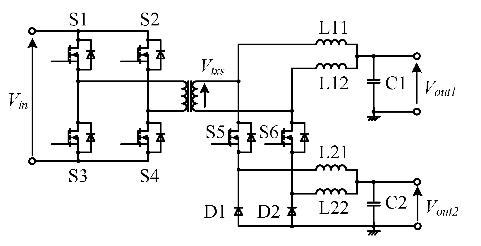
2. Circuit Configuration and Operation Principle

2.1. Circuit Configuration

Figure 1 presents the proposed circuit, consisting of a dual-output isolated DC/DC converter, with an input voltage Vin and two output voltages Vout1 and Vout2. The input/output isolation is realized by a high-frequency transformer. An H-bridge inverter consisting of S1–S4 is connected on the primary side of the transformer. A current doubler consisting of L11, L12, D1, D2, and C1 (Figure 2a) as well as an interleaved step-down chopper consisting of S5, S6, D1, D2, L21, L22, and C2 (Figure 2b) are connected on the secondary side of the transformer to form an integrated circuit. D1 and D2 are included in both circuits, thereby reducing the number of components. The H-bridge inverter and high-frequency transformer have conventional simple configurations, and the two outputs are achieved solely with the secondary side circuit.
The current paths L11 and L12 are for the current doubler output, and the current paths L21 and L22 are for the step-down chopper output. As a result, the conduction loss is reduced by half compared to a single-load current path. Because the phases of these currents are interleaved with a shift of 180°, the ripple frequencies at C1 and C2 become twice the inverter frequency, which reduces the capacity and thereby the volume of C1 and C2 by half. To maintain the interleaving symmetry, the inductance values of L11 and L12 and of L21 and L22 should be set to the same values.

2.2. Operation Principle

By switching S1 to S4, the H-bridge inverter generates three levels of voltage, namely +Vin, 0, and −Vin, and these voltages are applied on the primary side of the transformer. This circuit includes six operation modes based on the combination of the transformer secondary side voltage level Vtxs, which is transformed according to the turns ratio N1:N2, and the on–off states of S5 and S6.
Table 1 presents the states of Vtxs, S5, and S6, as well as the corresponding operation modes. In Table 1, “1”, “0”, or “−1” for Vtxs represent a voltage of a positive value, 0, or a negative among the three levels, respectively. Moreover, “-” for S5 and S6 indicates that it is irrelevant whether it is on or off. The reason for this irrelevance is that in these cases, a current flows from the source to the drain in S5 or S6; the current passes through the body diode even in the off state.
To explain each operation mode, Figure 3 depicts the ideal waveforms in the main part of the secondary side circuit in steady-state operation, whereas Figure 4 presents the equivalent circuit and current flow of each operation mode in the secondary side circuit. From the top, Figure 3 shows the transformer secondary side voltage Vtxs, the switching states of S5 and S6, the inductor currents on the current doubler side IL11 and IL12, and the inductor currents on the step-down chopper side IL21 and IL22.
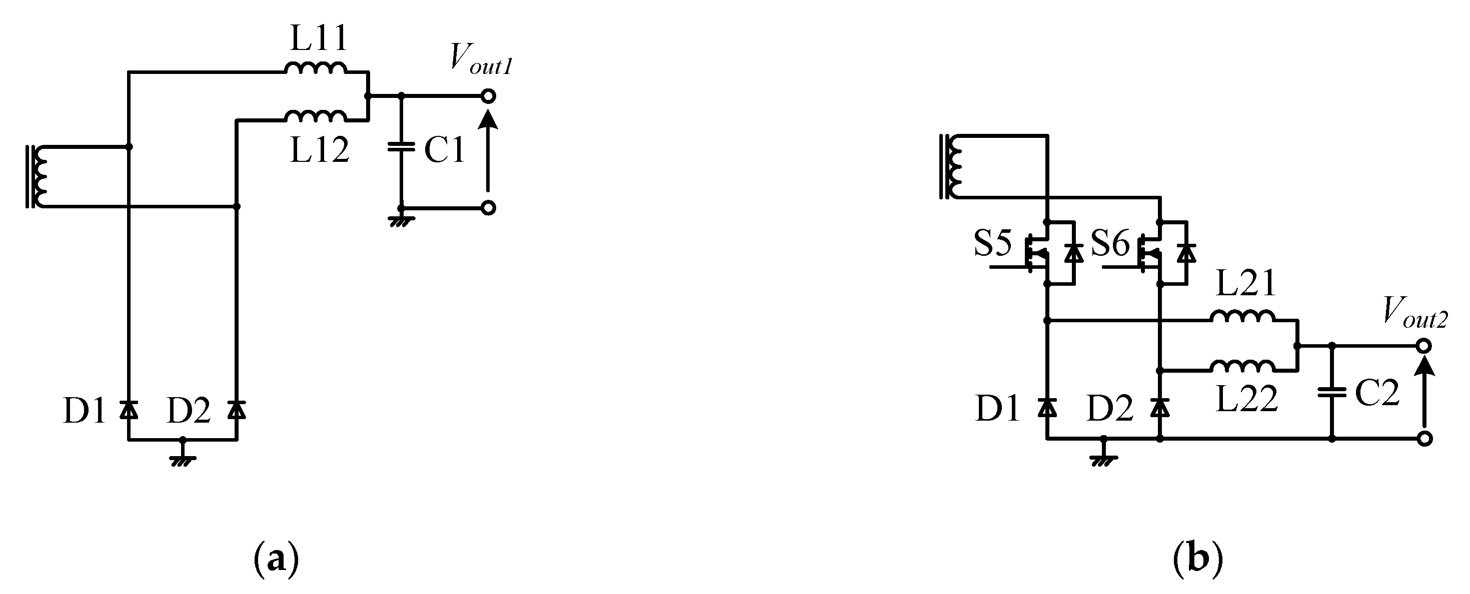
  • The operation of the secondary side circuit in each mode is described below.
    • Mode 1: Vtxs is positive and S5 is off (Figure 4a).
  • L11 is charged by Vtxs and L12, L21, and L22 discharge.
    • Mode 2: Vtxs is positive and S5 is on (Figure 4b).
  • As S5 is turned on, both L11 and L21 are charged by Vtxs, whereas L12 and L22 still discharge.
  • When Vtxs is 0, there is no power, and therefore, L11, L12, L21, and L22 all discharge.
    • Mode 4: Vtxs is negative and S6 is off (Figure 4d).
  • L12 is charged by Vtxs and L11, L21, and L22 discharge.
    • Mode 5: Vtxs is negative and S6 is on (Figure 4e).
  • As S6 is turned on, L12 as well as L22 are charged. L11 and L21 still discharge.
  • As in Mode 3, as Vtxs is 0, L11, L12, L21, and L22 discharge.
Table 2 displays the output voltages of the proposed circuit in the steady-state operation Vout1 and Vout2; the output currents Iout1 and Iout2; the output average inductor currents I L 11 ¯ , I L 12 ¯ , I L 21 ¯ , and I L 22 ¯ ; the inductor current ripple factors γL11, γL12, γL21, and γL22; and the capacitor ripple currents Δic1 and Δic2. In this case, d1 and d2 in the equations are duty ratios for the period in which Vtxs is positive or negative and for the period of Mode 2 or Mode 5, respectively, as illustrated in Figure 3. L1 and L2 are the inductance values of L11 or L12 and L21 or L22, respectively. R1 and R2 are the load resistance values of the current doubler and step-down chopper outputs, respectively. Moreover, T is the time of one cycle.
As indicated in Table 2, when Vin is constant, Vout1 and Vout2 are only dependent on the duty ratio corresponding to each of these. That is, the switching of S1 to S4 controls Vout1, and that of S5 and S6 controls Vout2. This means that Vout1 and Vout2 can be controlled independently; however, this is only possible when the circuit operates with the six operation modes described above. This means that the following condition must be satisfied:
d1 > d2.
If Equation (1) is not true (d1d2), S5 and S6 are always on, while the transformer is transmitting power from the primary side to the secondary side (when Vtxs is positive or negative). Consequently, there will be no means of controlling Vout2 and the dual-output converter cannot perform its function.

3. Actual Device Testing

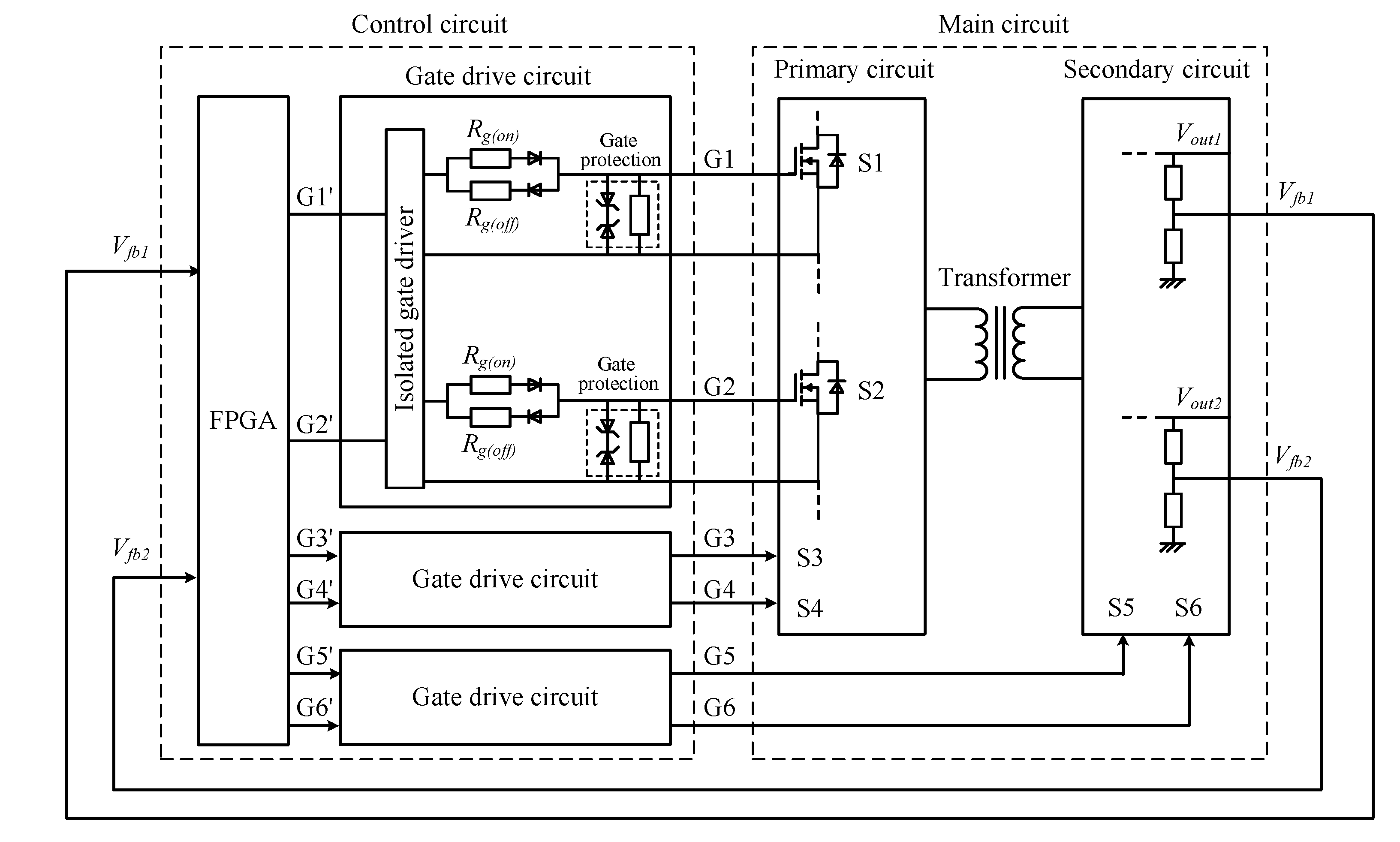
3.1. Main Circuit Configuration

Table 3 summarizes the specifications of the experimental circuit that was constructed to operate the proposed circuit at 400 kHz and 2 kW, the configuration and appearance of which are presented in Figure 5 and Figure 6, respectively. The input voltage was 300 V, the input capacitor was a 330 μF aluminum electrolytic capacitor, the output voltage on the current doubler side Vout1 was 48 V, and the output voltage on the step-down chopper side Vout2 was 12 V. The switching frequency was 400 kHz, as described previously. For the FPGA to generate control signals, XC7K70T-1FBG484C (Xilinx) with a clock cycle of 5 ns (200 MHz frequency) was used to obtain a sufficient time resolution for switching at 400 kHz (2.5 μs per cycle) to be obtained. A SiC MOSFET SCT3030AL (ROHM) with a short switching transition time was used for S1 to S6 considering the switching loss at 400 kHz. A SiC Schottky barrier diode FFSH4065A (ON Semiconductor) with an extremely short reverse recovery time was used for D1 and D2. Owing to the large current value in the secondary side circuit, S5, S6, D1, and D2 were connected in parallel and a snubber circuit was provided in light of the surge voltage in the off state. The transformer turns ratio was set to 4:2. The inductance values on the current doubler sides L11 and L12 were set to 15 μH, whereas those on the step-down chopper side L21 and L22 were set to 3 μH, considering the relationship among the ripple current amplitude, wire diameter, and core size. The output capacitor on the current doubler side C1 was set to 44 μF by connecting two 22 μF ceramic capacitors in parallel, whereas that on the step-down chopper side C2 was set to 188 μF by connecting four 47 μF ceramic capacitors in parallel. Because the experimental circuit was constructed with the aim of operating at 400 kHz and 2 kW, the selected switching devices as well as the designed transformers and inductors had plenty of room in terms of the breakdown voltage, current capacity, and saturation magnetic flux density.

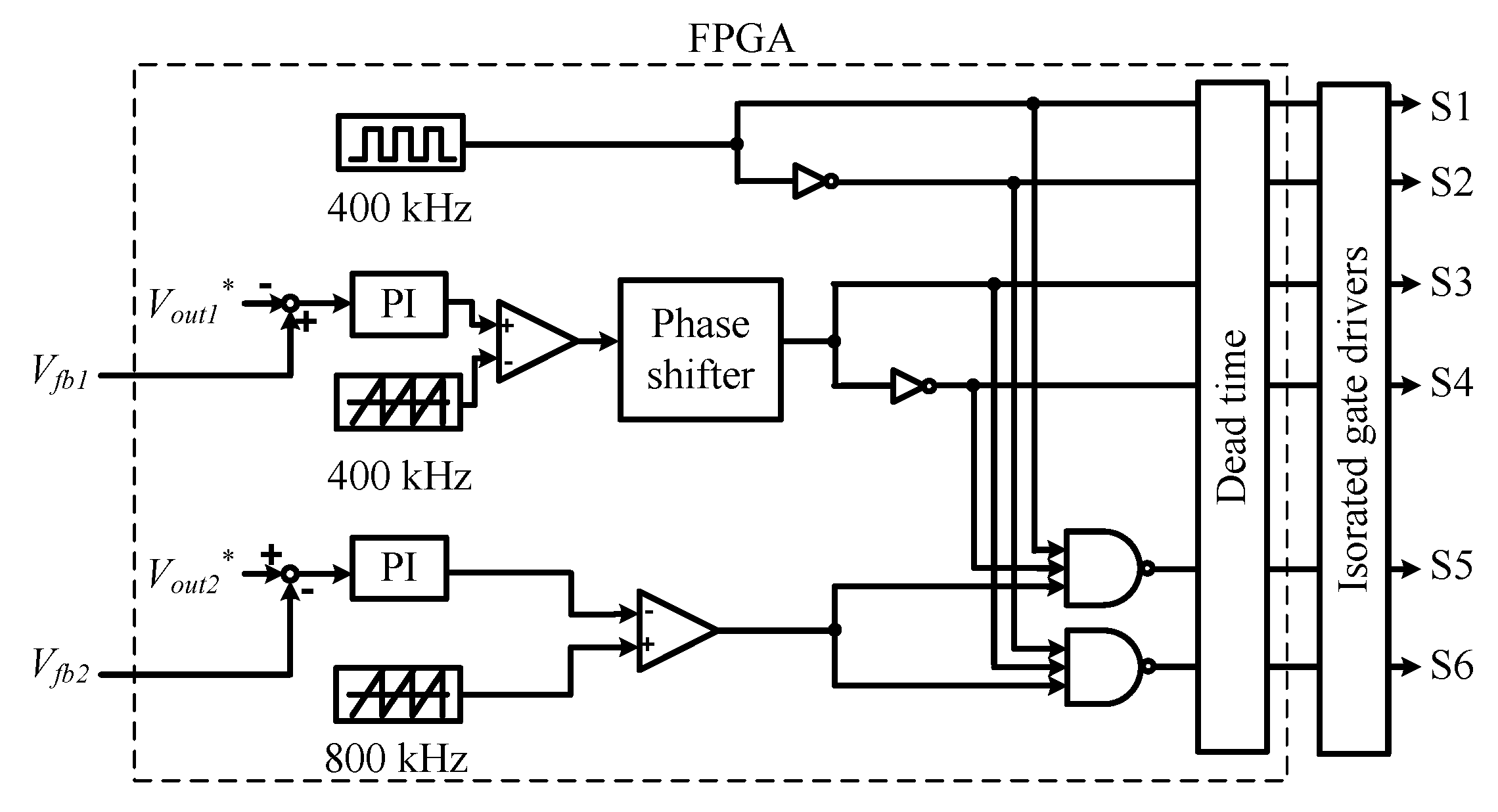
3.2. Control Circuit Configuration

Figure 7 depicts the control block diagram of the proposed circuit. All switching signals for S1 to S6 were generated by the FPGA (Appendix A), provided with appropriate dead time, and subsequently input to each gate via the isolated gate driver.
A square wave with a duty ratio of 0.5 and a frequency of 400 kHz was input to the gate of S1 and its inverted signal was input to the gate of S2. A phase-shifted signal of the S1 gate signal was input to the gate of S3 and its inverted signal was the gate signal of S4. This phase shift was quantified by the feedback of the output voltage on the current doubler side Vout1. In particular, the deviation between the divided voltage of Vout1, denoted by Vfb1, and the voltage command value Vout1* was input to the PI calculation unit. Subsequently, the output of the PI calculation unit was compared with the 400 kHz sawtooth wave synchronized with the S1 gate signal. The time corresponding to the pulse width of the comparison result was the phase-shift quantity.
The gate signals of S5 and S6 were derived from the feedback of the output voltage on the step-down chopper side. Similar to the process for the gate signals of S3 and S4, the first step was to calculate the difference between the divided voltage of the output voltage on the step-down chopper side Vout2, denoted by Vfb2, and the voltage command value Vout2*. Thereafter, the PI-calculated signal of this difference was compared with the 800 kHz sawtooth wave synchronized with the S1 gate signal. In this case, by setting the frequency of the sawtooth wave to twice the switching frequency, the pulse signal after comparison simultaneously generated the interleaved S5 and S6 switching signals. Subsequently, the inverted AND (NAND) of this pulse signal and the H-bridge inverter switching signal was created to enable the assigned switching of S5 when Vtxs was positive and that of S6 when Vtxs was negative, as demonstrated in Table 1 and Figure 3. For the modes in Table 1, in which the switching states of S5 and S6 were irrelevant, S5 and S6 were turned on to prevent loss owing to a current flow to the body diode.

3.3. Operation Points

Figure 8 presents the measured operation points and Table 4 displays the measurement instruments. There were five operation points for the output power on the current doubler side Pout1 between 200 and 1400 W using an inductive resistance of 8 Ω. There were four operation points for the output power on the step-down chopper side Pout2 between 150 and 500 W using a non-inductive resistance of 1 Ω. These 20 operation points in total were numbered from #01 to #20. An additional operation point #21 was set for an output of 2 kW, with output power on the current doubler side of 1421 W and output power on the step-down chopper side of 588 W. Based on these operation points, the measurements were performed as described in the following, where the numbers shown in Figure 8 are used to indicate the operation points.

3.4. Voltage Target Value Response Characteristics

Figure 9 displays the output voltages Vout1 and Vout2, and the output currents Iout1 and Iout2 from power-on to the steady state at operation point #21 with a total output power of 2058 W. As indicated in Figure 9, both the voltage and current took less than 1 s from power-on to settling, demonstrating the ability to control two different voltages at an output of 2 kW. The settled voltage values were 48.9 V for Vout1 and 12.4 V for Vout2. These were shifted from their command values of 48 and 12 V, which was caused by an error in the voltage dividing resistance ratio. In the steady state, the ripple voltage was ±1.3 V for both Vout1 and Vout2, whereas the ripple current was ±0.8 A for Iout1 and ±1.6 A for Iout2. The reason for the larger value of the ripple current Iout2 compared to Iout1 is that TCP303 (Tektronix), which was used to measure Iout2, has a lower resolution than TCP312A (Tektronix), which was used to measure Iout1.
In this experiment, the DC power supply was powered on after starting the control, and in this manner, the time to settle the voltage was constrained by the rise time of the DC power supply. That is, the proportional gain and time constant of the PI control unit, which were control parameters, were not involved in the behavior during power-on. These control parameters were optimized for the load disturbance response, as described later. If this circuit is used as on-board auxiliary power, the control will start with the battery voltage applied to the input. Accordingly, the time to reach a steady state will be shortened compared to that in this experiment, and the current and voltage overshoots are expected to be larger. To prevent this, countermeasures such as soft-start are necessary, which we consider as future tasks.

3.5. Operating Waveforms

Figure 10 presents the waveforms at four operation points during the steady-state operation: Vtxp, Vtxs, Itxp, Itxs, Vgs5, Vgs6, Vds5, Vds6, Vdiode1, Vdiode2, IL11, IL12, IL21, and IL22. Vtxp is the transformer primary side voltage, Itxp and Itxs are the transformer primary and secondary side currents, Vgs5 and Vgs6 are the gate-source voltages of S5 and S6, Vds5 and Vds6 are the drain-source voltages of S5 and S6, and Vdiode1 and Vdiode2 are the voltages across D1 and D2, respectively. In our setup, the oscilloscope had four channels and could not measure all waveforms simultaneously. Therefore, one channel was used to measure the Itxp waveform constantly as the trigger channel to synchronize the results of multiple measurements. The measurements were performed at four operation points: #01, where both Pout1 and Pout2 were minimized; #05, where only Pout1 was maximized based on #01; #16, where only Pout2 was maximized in the same manner; and #20, where both Pout1 and Pout2 were maximized. As can be observed from Figure 10, the operation proceeded at 2.5 μs (400 kHz) per cycle at all four operation points and there were indeed six operation modes, as described in Table 1 and Figure 3. These results confirm that the proposed circuit behaved as designed. Meanwhile, surges and associated ringing appeared in the secondary side circuit voltage at all operation points. The ringing frequencies were approximately 15 and 60 MHz, and these were considered as resonances owing to the transformer leakage inductance and the parasitic capacitance of S5 and S6 and D1 and D2, respectively. Noise was also observed at these frequencies in Vgs5 and Vgs6, indicating that high-frequency noise propagated in the entire secondary side circuit.

3.6. Detailed Operation Modes

To explain the detailed steady-state operation, Figure 11 presents the waveforms of Vtxp, Vtxs, Itxp, Itxs, Vgs5, Vgs6, Vds5, Vds6, Vdiode1, and Vdiode2 for a half period at three operation points, namely #01, #05, and #16, in an enlarged view. This half period corresponded to the ideal operation modes 1, 2, and 3, as previously described in Table 1, Figure 3 and Figure 4. Although the behavior varied slightly depending on the operation point, there were nine modes for the measured waveforms in total, which are divided by tn (n = 1 to 11) in Figure 11. In addition to the ideal operation modes 1, 2, and 3, six additional modes for state transitions were present. Table 5 displays the possible detailed operation modes for each operation point, and Figure 12 depicts the current path of the secondary side circuit in each operation mode. The operation in each mode is described below based on Figure 11 and Figure 12.
  • (t1 < t < t2) Period in which Vtxp began to increase (Figure 12a).
With the switching of the primary side inverter, Vtxp started to increase. Furthermore, S5, S6, D1, and D2 were in the on-state. The currents flowed from the source to the drain in S5 and from the drain to the source in S6, and a negative current flowed in the transformer. Because both ends of the transformer were connected to GND, a voltage was generated at Vtxs corresponding to L di/dt of the current path, but not corresponding to Vtxp.
2.
(t2 < t < t3) Period in which current flowed to S5 body diode (Figure 12b,c).
Vgs5 was turned off and the current flowing to S5 was commutated to the body diode. This mode continued until the current in the body diode became zero. Accordingly, a larger S5 current (larger output power) meant that this mode would last longer. In the case of #01, where Vgs5 was turned off, no current flowed from the source to the drain in S5; therefore, this mode did not exist for #01. In the cases of #05 and #16, owing to the different operation points, the commutated S5 body diode current flowed in different paths (Figure 12b,c).
Furthermore, in this mode, both ends of the transformer were connected to GND, and thus, no voltage corresponding to Vtxp was generated at Vtxs yet. Therefore, when the duty ratio was constant for Vtxp, when this mode was longer (the output power was larger), the duty ratio d1 for Vtxs was smaller. Because d1 was proportional to the output voltage Vout1 (Table 2), it attempted to take a constant value when Vout1 was constant. As a result, the duty ratio for Vtxp increased as the output power increased.
3.
(t3 < t < t5) Charging period for S5 parasitic capacitance Cds5 (Figure 12d–f).
The S5 body diode current became zero and Vtxs started to rise. This Vtxs acted as a power source to charge Cds5 (Figure 12d,f). This charging current was the peak current of Itxs and the current change generated a surge voltage at Vds5. As described later, this noise propagated to the entire secondary side circuit, including Vgs5 and Vgs6. A larger Pout2 resulted in a larger rate of change in the current. Therefore, the peak surge voltage was greater for #16 than for #01 and #05. Moreover, because the L21 current (D1 current) in the previous mode was small for #01 and #05, the charging current for Cds5 flowed to not only L21, but also to D1, causing the charging (t3 < t < t4) and discharging (t4 < t < t5) of the D1 parasitic capacitance CD1 (Figure 12d,e). This charging and discharging generated a voltage of approximately 70 V at Vdiode1. However, for #16, the D1 current in the previous mode was sufficiently large, and thus, the charging current for Cds5 did not charge CD1 (Figure 12f).
4.
(t5 < t < t6) Period corresponding to ideal operation mode 1 (Figure 12g).
S5 was off and D1 was on, and it operated in mode 1 of the ideal operation principle.
5.
(t6 < t < t7) Discharging period for Cds5 (Figure 12h).
Discharging of Cds5 was caused by turning on Vgs5, when the current flowing to L21 started to switch from the D1 current to the S5 current. The current continued to flow into S5 and D1 until S5 was on and completely switched; therefore, both ends of Vtxs were connected to GND again, reducing Vtxs.
6.
(t7 < t < t8) Charging period for CD1 (Figure 12i).
Once the discharging of Cds5 was complete and S5 was completely on, the current started to flow to L21 via S5. At the same time, the charging of CD1 started to turn off D1. The peak for Itxs was the charging current. The current change at this point generated a surge voltage at Vdiode1. The periods t6 to t8 were the time from the start of discharging Cds5 until the end of charging CD1. The current involved in the charging and discharging was dependent on Pout2. Consequently, #16, with a greater Pout2, had a longer t6 to t8 period than #01 and #05.
7.
(t8 < t < t9) Period corresponding to ideal operation mode 2 (Figure 12j).
D1 was completely off and it operated in mode 2 of the ideal operation principle.
8.
(t9 < t < t10) Discharging period for CD1 (Figure 12k).
By switching the primary side inverter, Vtxp and Vtxs decreased simultaneously. Accordingly, the current flowing from the transformer to L21 decreased. To compensate for this current loss, D1 was turned on. Discharging of CD1 occurred as a preliminary step.
9.
(t10 < t < t11) Period corresponding to ideal operation mode 3 (Figure 12l).
D1 was completely on, and it operated in mode 3 of the ideal operation principle.
The following half cycle behaved symmetrically with the nine modes described thus far. The behavior at each operation point during steady-state operation has been described with the series of operation modes above.

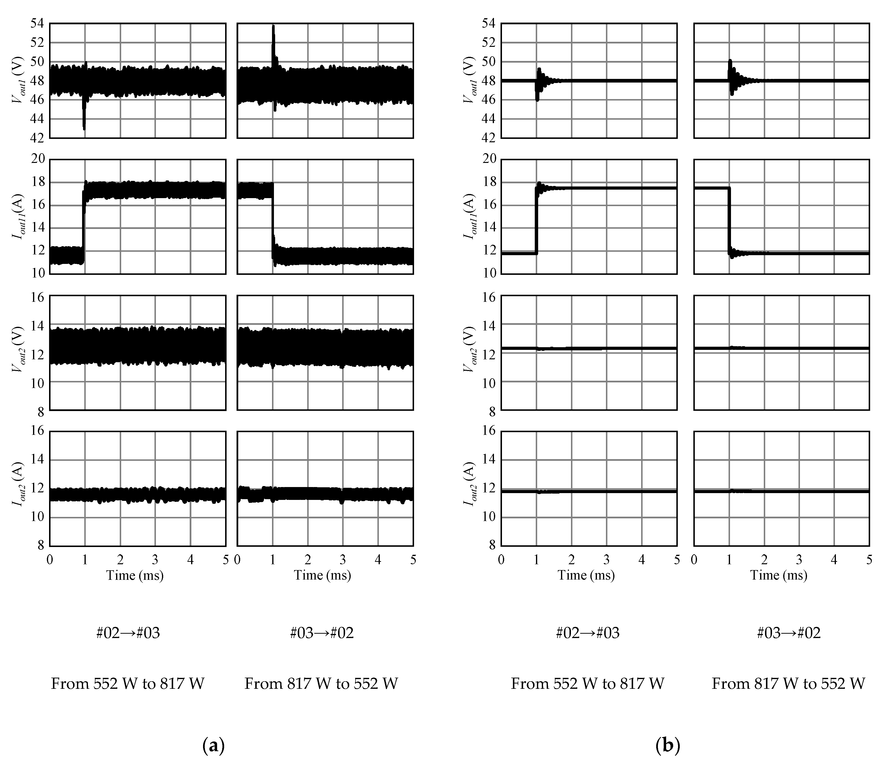
3.7. Load Disturbance Response Characteristics

Figure 13 and Figure 14 present the actual measurement results and simulation results of Vout1, Iout1, Vout2, and Iout2 when the operation point was switched during steady-state operation. Figure 15 shows the waveforms of Vtxs, Vout1, and Vout2 at operation point #08. In Figure 13, operation points #02 and #03 were switched to switch Pout1 only. In Figure 14, #03 and #08 were switched to switch Pout2 only. PSIM version 12.04 (Powersim) was used for the simulation. The parameters in Table 3 were used in the simulation, and an ideal device was assumed for the switching devices. Furthermore, no parasitic resistance, inductance, or capacitance existed in the simulation circuit. Figure 13 and Figure 14 verify the following: (1) when switching Pout1 and switching Pout2, it recovered to a steady state within 4 ms after the switching of the operation point, and (2) each waveform from the operation point switching to the recovered steady state was in good agreement with the simulated waveform. Based on these results, the load variation control was realized as designed. Compared to the simulation results, the actual measurement results exhibited greater superimposed noise in the voltage and current. These noises were in accordance with the surge timing of Vtxs, as illustrated in Figure 15. As indicated above, a Vtxs surge was generated at the switching timing of S5, S6, D1, and D2, thereby demonstrating that the switching noises in the secondary side circuit propagated to the output voltage. This indicates the noise propagation via paths that could not be absorbed by the output smoothing capacitors C1 and C2, revealing the layout design issue of the secondary side circuit.
The measurement results of the voltage target value response and load disturbance response characteristics verified the behavior of the proposed circuit as designed. Thus, despite certain issues, the 400 kHz, 2 kW dual-output DC/DC converter was demonstrated.

4. Efficiency and Loss Evaluation

4.1. Efficiency Characteristics

The input power Pin and output power Pout1 and Pout2 were measured using a power analyzer, namely WT1800 (YOKOGAWA). The efficiency η was measured at each operation point of the test circuit based on the following equation:
η = P o u t 1 + P o u t 2 P i n .
The measurement results are presented in Figure 16. The efficiency increased as Pout1 increased, whereas it decreased as Pout2 increased. The maximum efficiency was 81.3% at #05, where Pout1 was the maximum and Pout2 was the minimum. The minimum efficiency was 65.1% at #16, where Pout2 was the maximum and Pout1 was the minimum. These results demonstrate the significant influence of the load loss of Pout2 on the reduced efficiency.

4.2. Loss Characteristics

The voltage and current of the transformer on the primary and secondary sides were measured using the devices in Table 4 for 100 μs. Moreover, the power Ptxp and Ptxs of the transformer on the primary and secondary sides, respectively, were calculated based on the following equation:
P = 1 40 T 0 40 T v ( t ) i ( t ) Δ T ,
where P is the power, and v(t) and i(t) are the measured voltage and current, respectively. Furthermore, T is the time of one cycle and ΔT is the time resolution of the oscilloscope with the values of T = 2.5 μs and ΔT = 0.1 ns. The calculated Ptxp and Ptxs as well as the measured Pin, Pout1, and Pout2 were used to divide the total loss Wtotal into three parts: the inverter loss Winv, transformer loss Wtx, and secondary side loss Wsec. The derivation formula for each loss is displayed in Table 6. Owing to the convenience of the measurement system, the time of the data acquisition by the power analyzer and the oscilloscope was not simultaneous but differed in each case.
The results of the loss separation are illustrated in Figure 17. The subjects of the loss separation were operation points #01, #05, #16, and #20, which had the maximum or minimum Pout1 or Pout2, respectively. The left axis indicates the power loss, and the right axis is the square of the total output current Iout1 + Iout2. The right axis is provided to indicate the conduction loss. As illustrated in Figure 17, the total loss and those at the different locations increased in the order of #01 < #05 < #16 < #20. This trend was consistent with the square of the total output current. Thus, it was demonstrated that the conduction loss was dominant compared to the iron loss or switching loss at the 400 kHz operation. Moreover, the secondary side loss accounted for more than half of the total loss at all operation points. Therefore, to improve the efficiency of the test circuit, it is effective to reduce the conduction loss in the secondary side circuit.
A main reduction measure for the secondary side circuit conduction loss is the reduction in the on-resistance of the switching device. For example, S5 and S6 can be replaced with a low on-resistance device that matches the operation conditions, whereas D1 and D2 can be replaced with MOSFET that matches the operation conditions and performs synchronous rectification control. Another measure is to change the transformer turns ratio and to increase the step-down ratio, which enables devices with a lower breakdown voltage to be selected and results in a further reduction in the on-resistance. However, in this case, overly increasing the step-down ratio will lead to a reduction in the upper limit of the output power on the 48 V side.

5. Conclusions

In this paper, a novel dual-output isolated DC/DC converter using an integrated circuit of a current doubler and step-down chopper on the secondary side of the high-frequency transformer was proposed. Although the control method becomes more complex, the proposed circuit is expected to have a smaller size and higher efficiency compared to the existing circuits. For automotive use, a maximum output power was 2 kW and switching frequency was 400 kHz, which is a higher frequency compared to the existing studies. The objective of this study was to operate, evaluate, and identify issues for the proposed circuit with the above condition.
As a result of the actual prototype circuit test, both the voltage target response characteristics and load disturbance response characteristics were observed as designed, confirming the validity of the proposed circuit. Moreover, we identified two solutions to specific issues: (1) soft-start control at power-on and (2) a reduction in noise propagation to the output by improving the layout.
The maximum and minimum efficiencies of this circuit were 81.3 and 61.5%, respectively. Larger output power on the current doubler side and smaller output power on the step-down chopper side resulted in higher efficiency. The loss analysis demonstrated that the loss on the secondary side accounted for more than 50%, suggesting that it is effective to reduce the on-resistance of the switching device on the secondary side to improve the efficiency.
Although we demonstrated the feasibility of the proposed circuit, we did not show that it can be compact and highly efficient as auxiliary power for EVs, PHVs, and FCVs owing to the nature of the prototype. Therefore, future tasks for improving the efficiency and downsizing include the optimization of the devices, parameters (switching device, transformer turns ratio, core material, core shape, and inductance value), and layout.

Author Contributions

Conceptualization, Y.M., T.N.; methodology, Y.M., T.N.; software, Y.M.; validation, Y.M., T.N.; formal analysis, Y.M.; investigation, Y.M.; data curation, Y.M.; writing—original draft preparation, Y.M.; writing—review and editing, Y.M., T.N.; supervision, T.N.; project administration, N.T., M.I. All authors have read and agreed to the published version of the manuscript.

Funding

This research received no external funding.

Conflicts of Interest

The authors declare no conflict of interest.

Appendix A

Figure A1 indicates whole feedback loop image of the proposed circuit. Vfb1 and Vfb2, the feedback voltages of the main circuit output voltage Vout1 and Vout2, are input to FPGA. G1′~G6′ are generated by FPGA and input to the gate drive circuits. Gate signals G1~G6 adjusted by isolated gate drivers and gate resistances Rg in the gate drive circuits input to each gate of S1~S6 in the main circuit, respectively. S1~S4 control Vout1 (Vfb1) and S5, S6 control Vout2 (Vfb2), respectively. This is a whole feedback loop image of the proposed circuit.
Figure A1. Whole feedback loop image of the proposed circuit.
Wevj 11 00078 g0a1

References

  1. IEA–International Energy Agency, CO2 Emissions from Fuel Combustion: Overview. Available online: https://www.iea.org/reports/co2-emissions-from-fuel-combustion-overview (accessed on 2 November 2020).
  2. IEA–International Energy Agency, Global EV Outlook 2020. Available online: https://www.iea.org/reports/global-ev-outlook-2020 (accessed on 2 November 2020).
  3. Krismer, F.; Kolar, J.W. Efficiency-Optimized High-Current Dual Active Bridge Converter for Automotive Applications. IEEE Trans. Ind. Electron. 2012, 59, 2745–2760. [Google Scholar] [CrossRef]
  4. Hou, R.; Magne, P.; Bilgin, B.; Emadi, A. A topological evaluation of isolated DC/DC converters for Auxiliary Power Modules in Electrified Vehicle applications. In Proceedings of the 2015 IEEE Applied Power Electronics Conference and Exposition (APEC), Charlotte, NC, USA, 15–19 March 2015. [Google Scholar]
  5. Rhodes, K.; Kok, D.; Sohoni, P.; Perry, E.; Kraska, M.; Wallace, M. Estimation of the Effects of Auxiliary Electrical Loads on Hybrid Electric Vehicle Fuel Economy. SAE Tech. Pap. 2017, 1, 1155. [Google Scholar]
  6. Adriano, S.; Chiara, F.; Fabrizio, Z.; Alessandro, D.; Fabio, O.; Annalisa, D. Experimental Analysis of the Auxiliaries Consumption in the Energy Balance of a Pre-series Plug-in Hybrid-electric Vehicle. Energy Procedia 2014, 45, 779–788. [Google Scholar] [CrossRef] [Green Version]
  7. Teratani, T. Impact of DC48V on Automotive Power Supply Systems—Comparison with DC42V and Future View under DC60V—. IEEJ Trans. Ind. Appl. 2015, 135, 892–897. [Google Scholar] [CrossRef]
  8. Hayslett, S.; Maanen, K.V.; Wenzel, W.; Husain, T. The 48-V Mild Hybrid: Benefits, Motivation, and the Future Outlook. IEEE Electrif. Mag. 2020, 8, 11–17. [Google Scholar] [CrossRef]
  9. Chen, G.; Deng, Y.; Dong, J.; Hu, Y.; Jiang, L.; He, X. Integrated Multiple-Output Synchronous Buck Converter for Electric Vehicle Power Supply. IEEE Trans. Veh. Technol. 2017, 66, 5752–5761. [Google Scholar] [CrossRef]
  10. Matsushita, Y.; Noguchi, T.; Kimura, O.; Sunayama, T. Current-doubler based multiport DC/DC converter with galvanic isolation. In Proceedings of the 2017 IEEE 12th International Conference on Power Electronics and Drive Systems (PEDS), Honolulu, HI, USA, 12–15 December 2017. [Google Scholar]
  11. Jones, E.A.; de Rooij, M.; Biswas, S. GaN Based DC-DC Converter for 48 V Automotive Applications. In Proceedings of the 2019 IEEE Workshop on Wide Bandgap Power Devices and Applications in Asia (WiPDA Asia), Taipei, Taiwan, 23–25 May 2019. [Google Scholar]
  12. Martinez-heredia, J., M.; Colodro, F.; Mora-Jiménez, J.L.; Remujo, A.; Soriano, J.; Esteban, S. Development of GaN Technology-Based DC/DC Converter for Hybrid UAV. IEEE Access 2020, 8, 88014–88025. [Google Scholar] [CrossRef]
  13. Mitova, R.; Ghosh, R.; Mhaskar, U.; Klikic, D.; Wang, M.; Dentella, A. Investigations of 600-V GaN HEMT and GaN Diode for Power Converter Applications. IEEE Trans. Power Electron. 2014, 29, 2441–2452. [Google Scholar] [CrossRef]
  14. Huang, X.; Lee, F.C.; Li, Q.; Du, W. High-Efficiency GaN-Based Interleaved CRM Bidirectional Buck/Boost Converter with Inverse Coupled Inductor. IEEE Trans. Power Electron. 2016, 31, 4343–4352. [Google Scholar] [CrossRef]
  15. Imaoka, J.; Okamoto, K.; Kimura, S.; Noah, M.; Martinez, W.; Yamamoto, M.; Shoyama, M. A Magnetic Design Method Considering DC-Biased Magnetization for Integrated Magnetic Components Used in Multiphase Boost Converters. IEEE Trans. Power Electron. 2018, 33, 3346–3362. [Google Scholar] [CrossRef]
  16. Sugimura, K.; Yabu, N.; Sonehara, M.; Sato, T. Novel Method for Making Surface Insulation Layer on Fe-Based Amorphous Alloy Powder by Surface-Modification Using Two-Step Acid Solution Processing. IEEE Trans. Magn. 2018, 54, 2801805. [Google Scholar] [CrossRef]
  17. Liang, W.; Raymond, L.; Rivas, J. 3-D-Printed Air-Core Inductors for High-Frequency Power Converters. IEEE Trans. Power Electron. 2016, 31, 52–64. [Google Scholar] [CrossRef]
  18. Inoue, S.; Itoh, K.; Ishigaki, M.; Sugiyama, T. Magnetically integrated isolated bidirectional three-port DC-DC converter. In Proceedings of the 2017 19th European Conference on Power Electronics and Applications (EPE’17 ECCE Europe), Warsaw, Poland, 11–14 September 2017. [Google Scholar]
  19. Dao, N.D.; Lee, D.; Phan, Q.D. High-Efficiency SiC-Based Isolated Three-Port DC/DC Converters for Hybrid Charging Stations. IEEE Trans. Power Electron. 2020, 35, 10455–10465. [Google Scholar] [CrossRef]
  20. Tang, Y.; Lu, J.; Wu, B.; Zou, S.; Ding, W.; Khaligh, A. An Integrated Dual-Output Isolated Converter for Plug-in Electric Vehicles. IEEE Trans. Veh. Technol. 2018, 67, 966–976. [Google Scholar] [CrossRef]
Figure 1. Proposed dual-output DC/-DC converter.
Wevj 11 00078 g001
Figure 2. Decomposed configuration of secondary circuit: (a) current doubler; (b) step-down chopper.
Wevj 11 00078 g002
Figure 3. Ideal waveforms of each operation mode.
Wevj 11 00078 g003
Figure 4. Equivalent circuit and current flow of each operation mode in secondary circuit: (a) Mode 1; (b) Mode 2; (c) Mode 3; (d) Mode 4; (e) Mode 5; (f) Mode 6.
Wevj 11 00078 g004
Figure 5. Configuration of experimental test circuit.
Wevj 11 00078 g005
Figure 6. Experimental circuit setup: (a) main circuit with control circuit; (b) main circuit without control circuit.
Wevj 11 00078 g006
Figure 7. Control block diagram of proposed circuit.
Wevj 11 00078 g007
Figure 8. Measured operation points.
Wevj 11 00078 g008
Figure 9. Dual-port output waveforms.
Wevj 11 00078 g009
Figure 10. Waveforms of proposed circuit: (a) #01; (b) #05; (c) #16; (d) #20.
Wevj 11 00078 g010
Figure 11. Waveforms of proposed circuit for half period: (a) #01; (b) #05; (c) #16.
Wevj 11 00078 g011
Figure 12. Current path of experimental circuit in each operation mode; (a) Mode 1; (b) Mode 2-1; (c) Mode 2-2; (d) Mode 3-1a; (e) Mode 3-1b; (f) Mode 3-2; (g) Mode 4; (h) Mode 5; (i) Mode 6; (j) Mode 7; (k) Mode 8; (l) Mode 9.
Wevj 11 00078 g012
Figure 13. Results of Pout1 dynamic response test when Pout2 = 141 W: (a) measurement results; (b) simulation results.
Wevj 11 00078 g013
Figure 14. Results of Pout2 dynamic response test when Pout1 = 825 W: (a) measurement results; (b) simulation results.
Wevj 11 00078 g014
Figure 15. Experimental waveforms of Vtxs, Vout1, and Vout2 at #08.
Wevj 11 00078 g015
Figure 16. Results of efficiency measurements.
Wevj 11 00078 g016
Figure 17. Loss analysis results.
Wevj 11 00078 g017
Table 1. Operation modes of proposed circuit.
Operation Mode123456
Vtxs110−1−10
S5offon----
S6---offon-
Table 2. Theoretical formulas of proposed circuit.
SymbolValueSymbolValue
Vout1 d 1 N 2 V i n N 1 Vout2 d 2 N 2 V i n N 1
Iout1 d 1 N 2 V i n N 1 R 1 Iout2 d 2 N 2 V i n N 1 R 2
I L 11 ¯
I L 12 ¯
d 1 N 2 V i n 2 N 1 R 1 I L 21 ¯
I L 22 ¯
d 2 N 2 V i n 2 N 1 R 2
γL11
γL12
2 R 1 ( 1 - d 1 ) T L 1 γL21
γL22
2 R 2 ( 1 - d 2 ) T L 2
Δic1 R 1 ( 1 - d 1 ) T I o u t 1 L 1 Δic2 R 2 ( 1 - d 2 ) T I o u t 2 L 2
Table 3. Parameters of experimental circuit.
ParameterValue
Vin300 V
Cin330 μF
Vout1 (current doubler side)48 V
Vout2 (step-down chopper side)12 V
Switching frequency400 kHz (T = 2.5 μs)
FPGAXC7K70T-1FBG484C (Xilinx)
Clock frequency of FPGA200 MHz
S1, S2, S3, S4, S5, S6SCT3030AL (ROHM)
D1, D2FFSH4065A (ON Semiconductor)
Transformer turns ratioN1:N2 = 4:2
L11 and L1215 μH
L21 and L225 μH
C144 μF
C2188 μF
Table 4. Measurement instruments.
InstrumentModel Number
OscilloscopeHDO6104A-MS (TELEDYNE)
Voltage differential probe700924 (YOKOGAWA)
Current probe (<30 A)TCP312A (Tektronix)
Current probe (>30 A)TCP303 (Tektronix)
Deskew calibration sourceDCS025 (TELEDYNE)
Table 5. Detailed operation modes.
Operation PointOperation Mode
12-12-23-1a3-1b3-2456789
t1~t2t2~t3t3~t5t5~t6t6~t7t7~t8t8~t9t9~t10t10~t11
#01
#05
#16
Table 6. Loss calculations.
PartSymbolEquation
Total lossWtotalPin − (Pout1 + Pout2)
Inverter lossWinvPinPtxp
Transformer lossWtxPtxpPtxs
Secondary side lossWsecWtotal − (Winv + Wtx)
Publisher’s Note: MDPI stays neutral with regard to jurisdictional claims in published maps and institutional affiliations.

