
Design of an SoC Based on 32-Bit RISC-V Processor with Low-Latency Lightweight Cryptographic Cores in FPGA


Abstract
1. Introduction
2. Related Works
3. RISC-V Processor
3.1. RISC-V ISA
- Free: RISC-V ISA and its surrounding development projects are mostly open-source.
- Simple: RISC-V is much smaller than other commercial ISAs.
- Modular: RISC-V has a small standard base ISA with multiple standard extensions.
- Stable: The base and many extensions of the ISA are already standardized and frozen. No significant changes are expected.
- Extensibility: specialized instructions can be added, based on extensions.
3.2. VexRiscv Processor
4. Cryptographic Algorithms
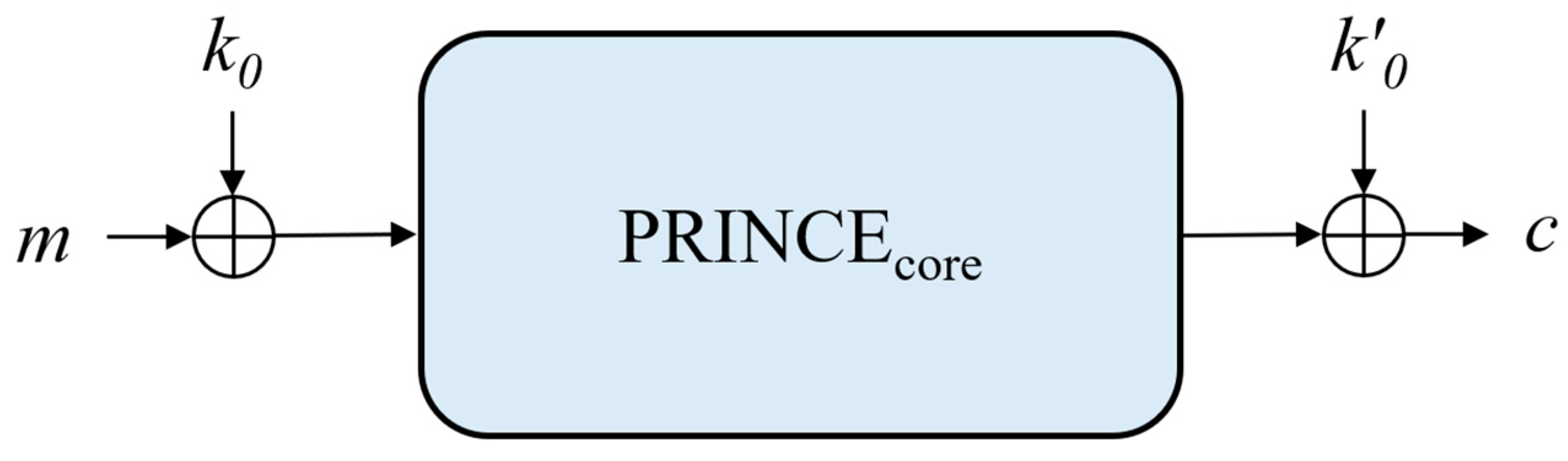
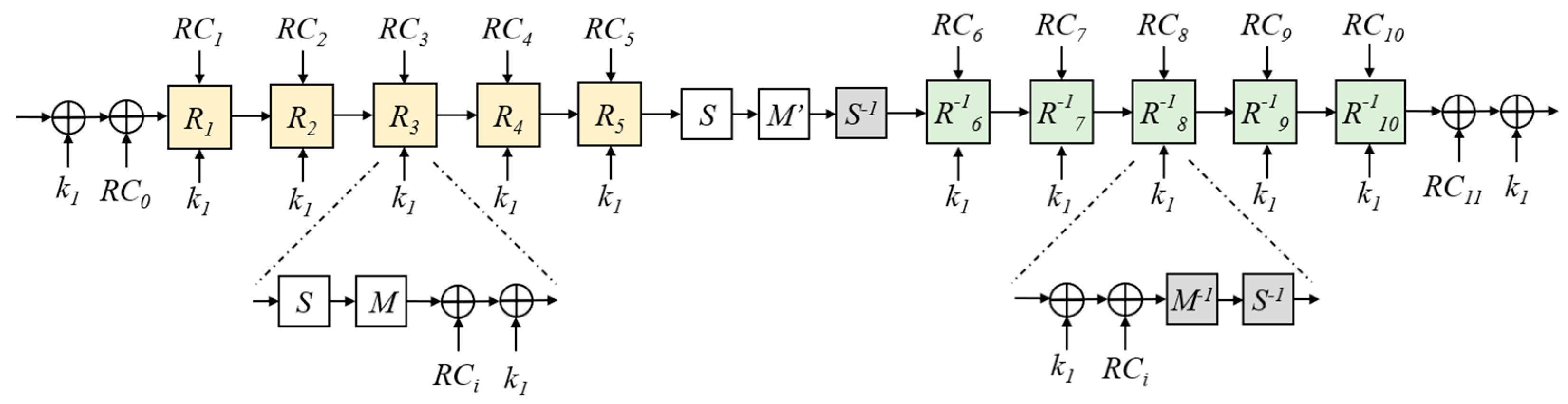
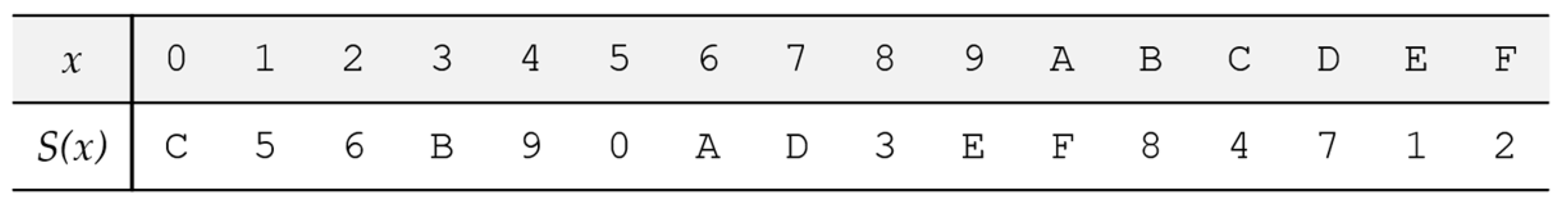
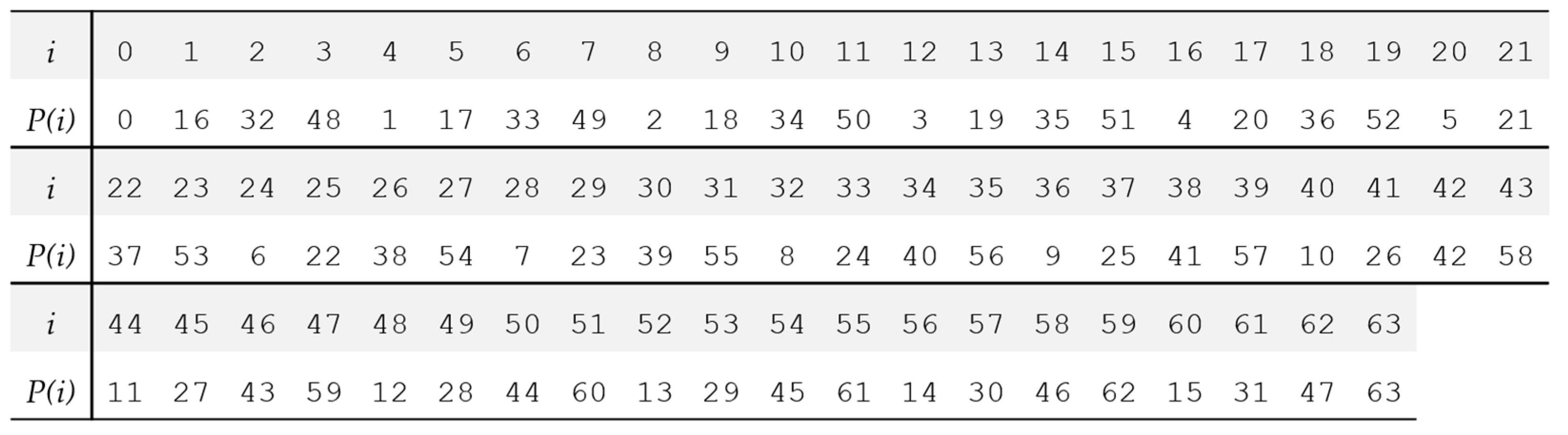
4.1. PRINCE
4.2. PRESENT-80
- Rotate the key register K by 61-bit positions to the left.
- The four leftmost bits are substituted using the S-box.
- The bits of [k19k18k17k16k15] are XORed with the current round number counter (5 bits).
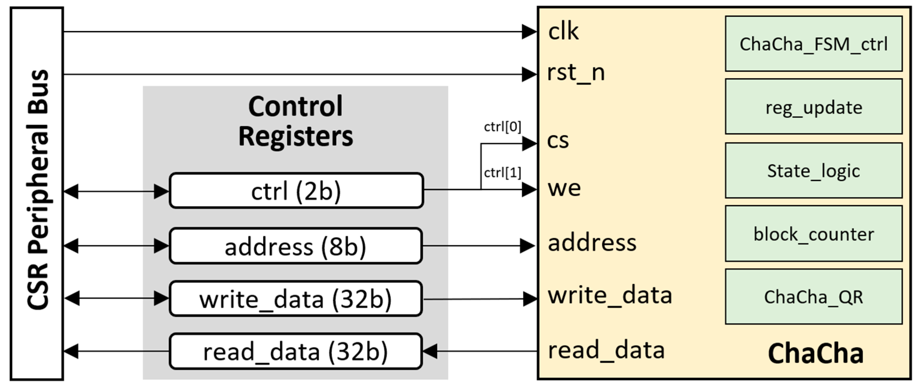
4.3. ChaCha
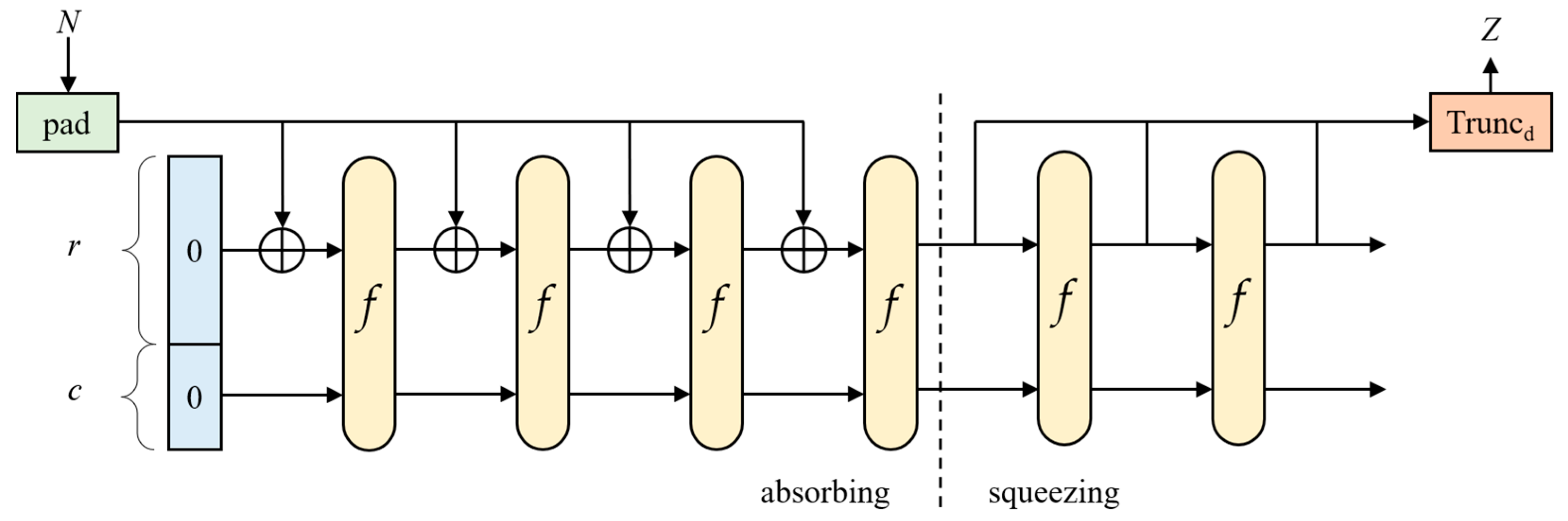
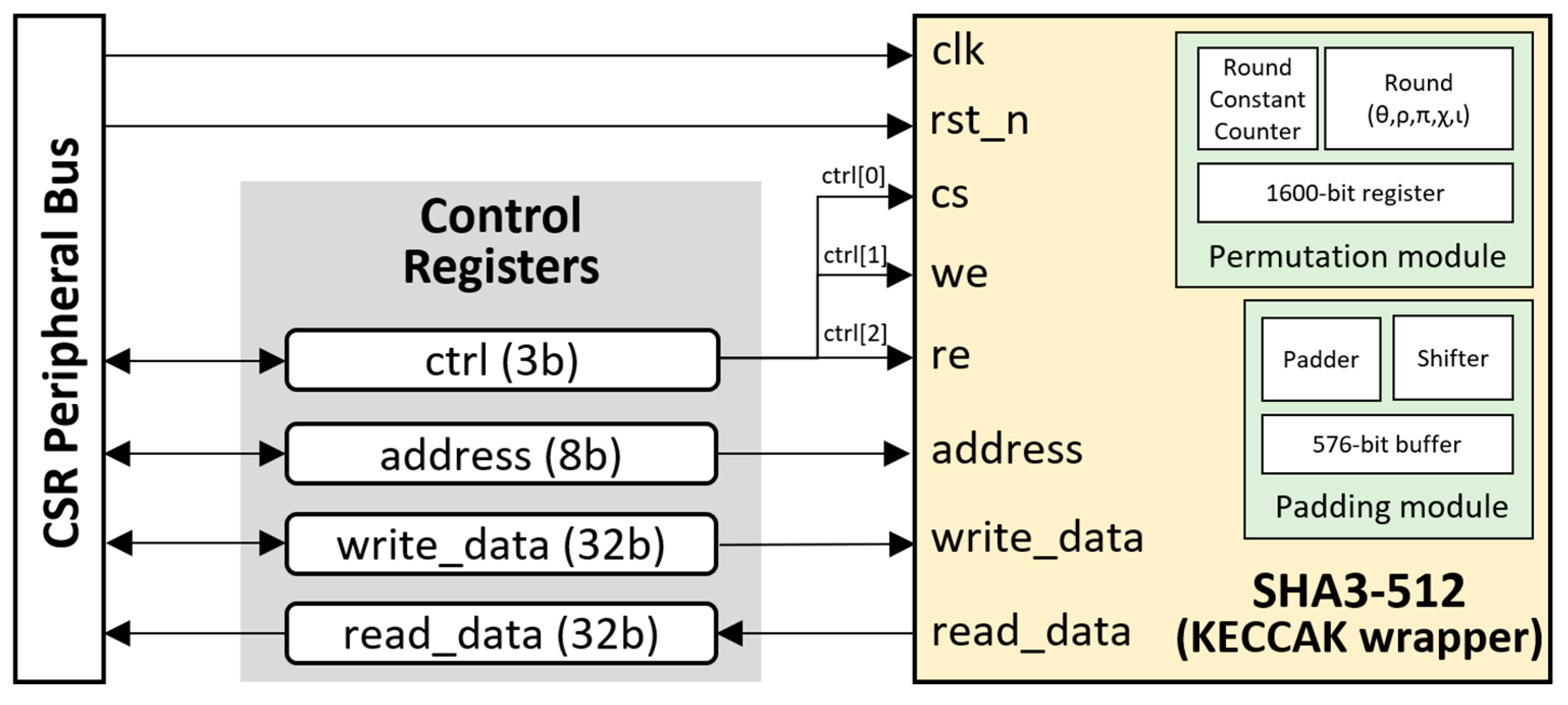
4.4. SHA3-512
5. Implementations
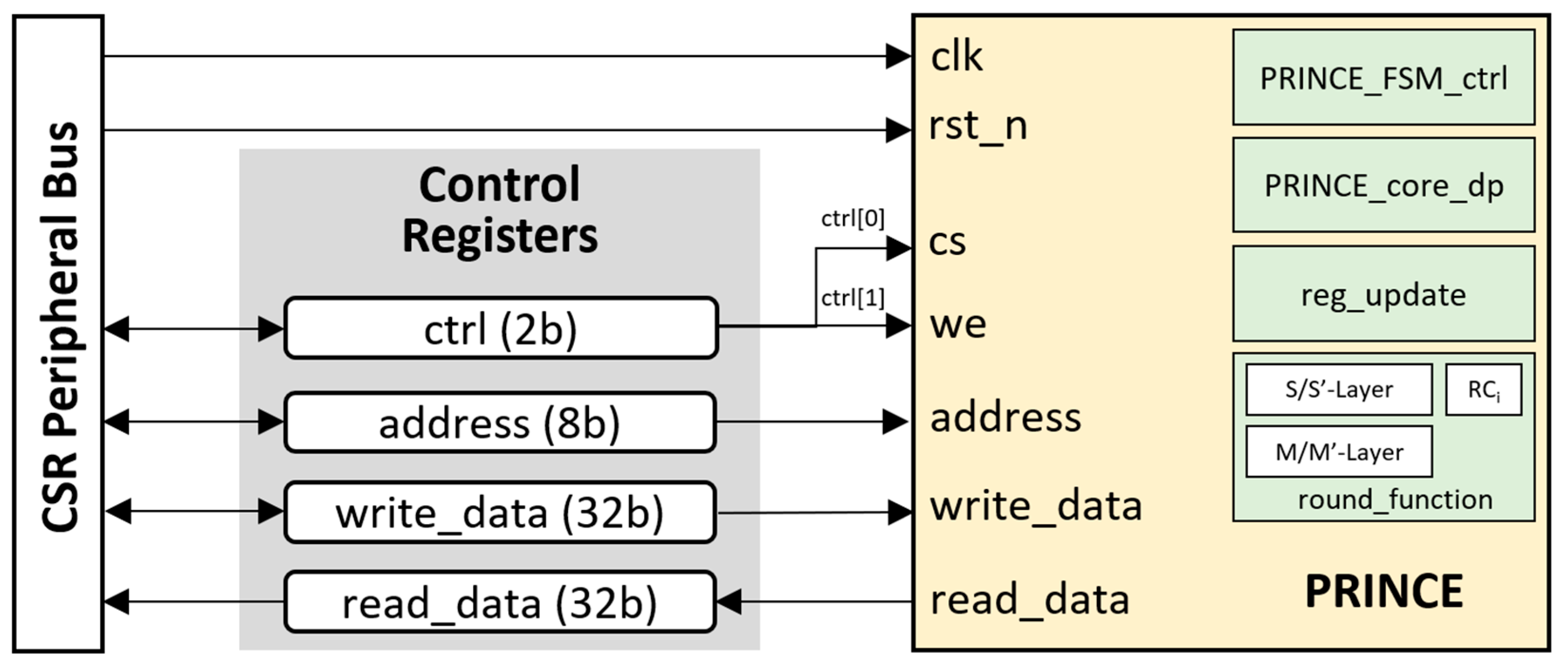
5.1. The PRINCE Accelerator Core
- “prince_write_to_address(address, data)”: This function prepares the “write_data” and “address” for the accelerator core and then simulates the core with “cs” and “we” for the writing process. This function writes 32-bit data or configuration values for the 8-bit address in the PRINCE accelerator core.
- “prince_read_from_address(address)”: The function simulates the core with “cs” and “we” for the reading process and reads the output from the accelerator core after preparing the “address” and ignoring the “write_data”. This function reads 32-bit data from an 8-bit address in the PRINCE accelerator core.
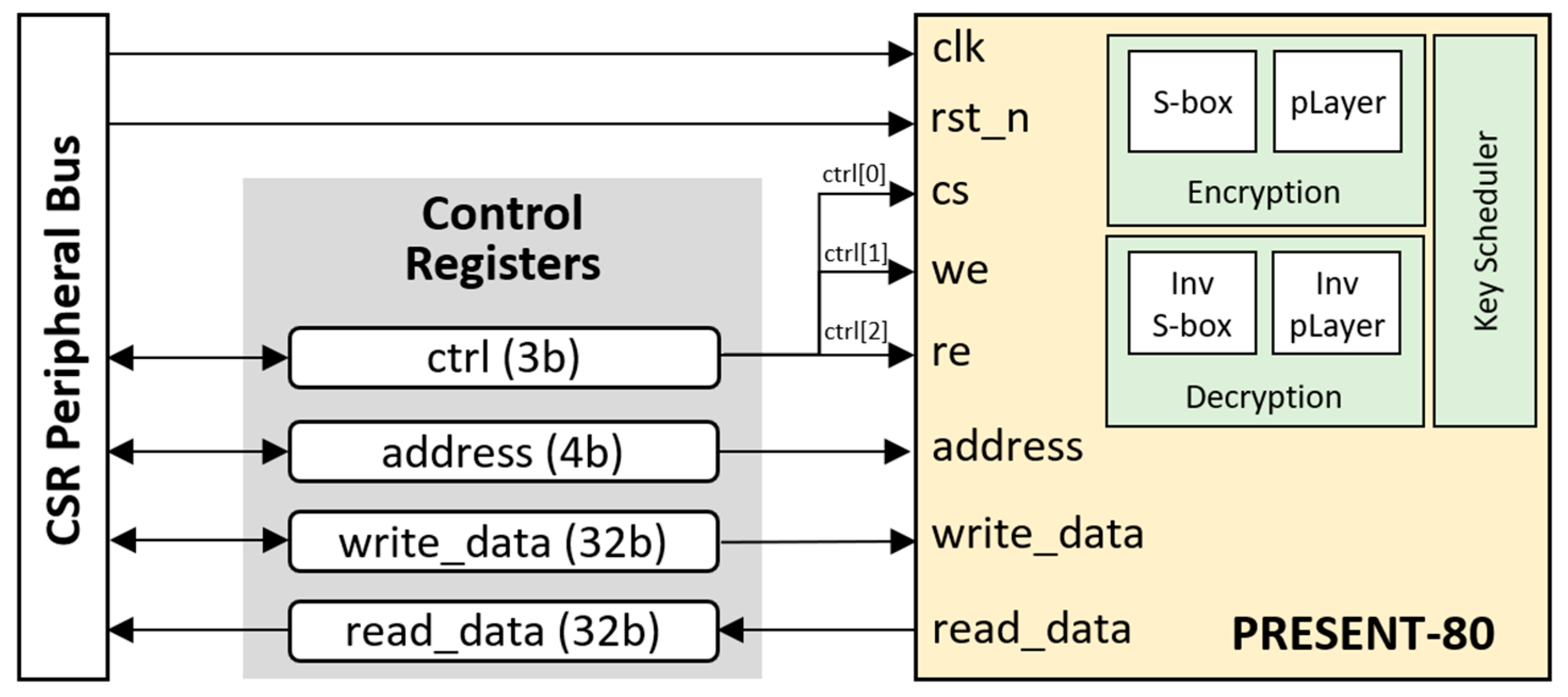
5.2. The PRESENT-80
5.3. The ChaCha Accelerator Core
5.4. The SHA3-512 Accelerator Core
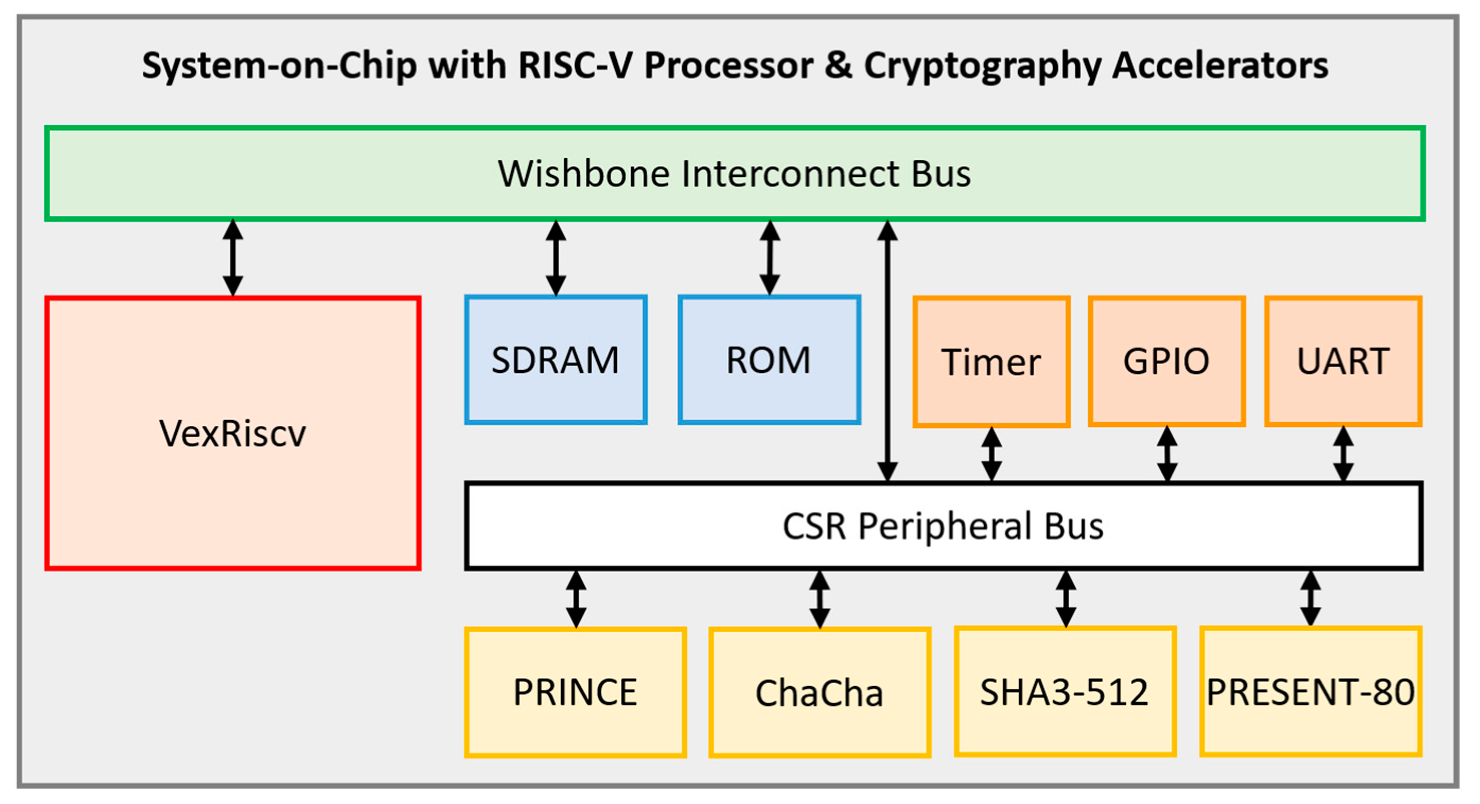
5.5. The System-on-Chip
- Single-core 32-bit VexRiscv processor (RV32IM), 32-bit Wishbone Bus with 4 GB address space, 8 KB L1 cache (4 KB data cache and 4 KB instruction cache), and 8 KB L2 cache.
- Peripherals: UART, SPI, GPIO.
- Custom cryptographic accelerator cores for PRINCE, PRESENT-80, ChaCha, and SHA3-512.
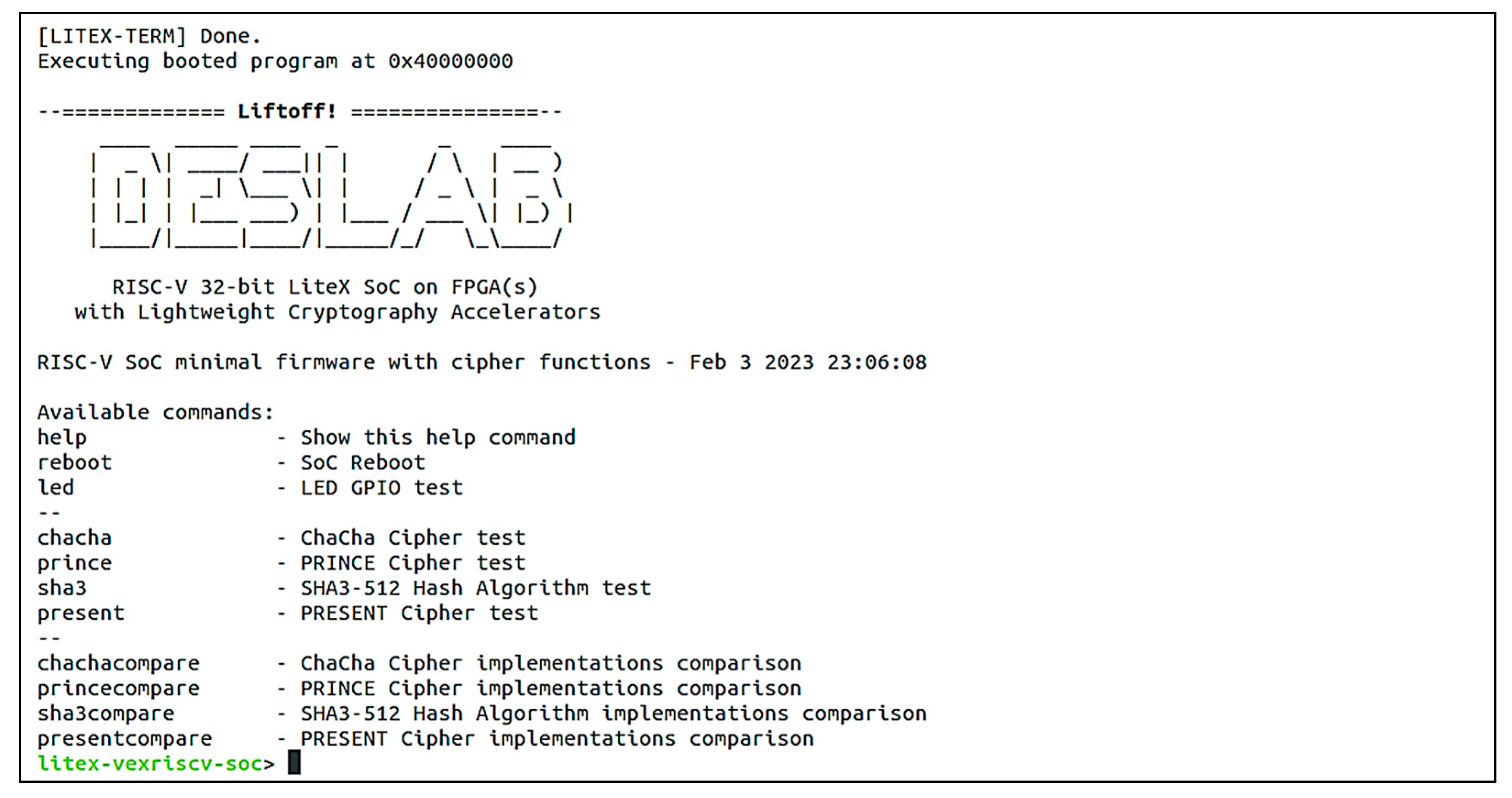
6. Experimental Results
6.1. FPGA Implementation Results
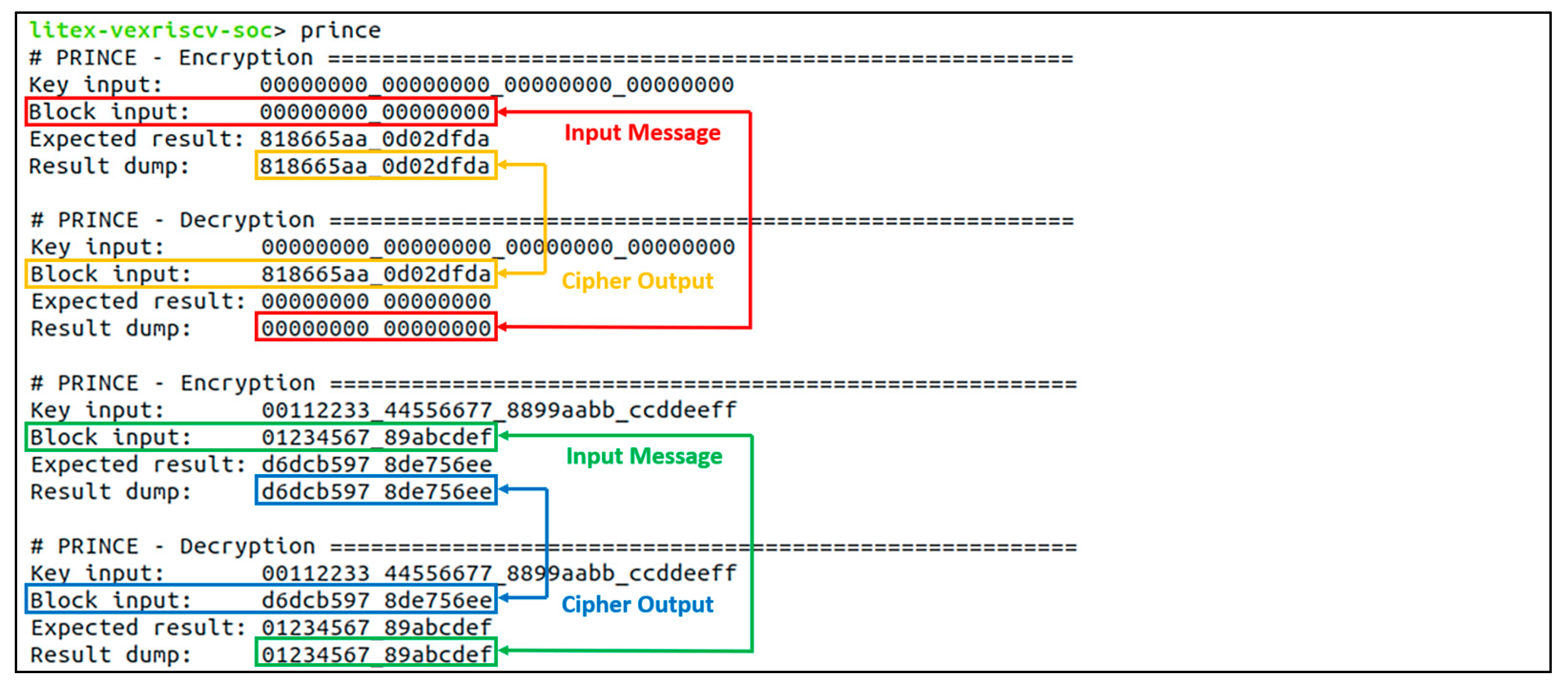
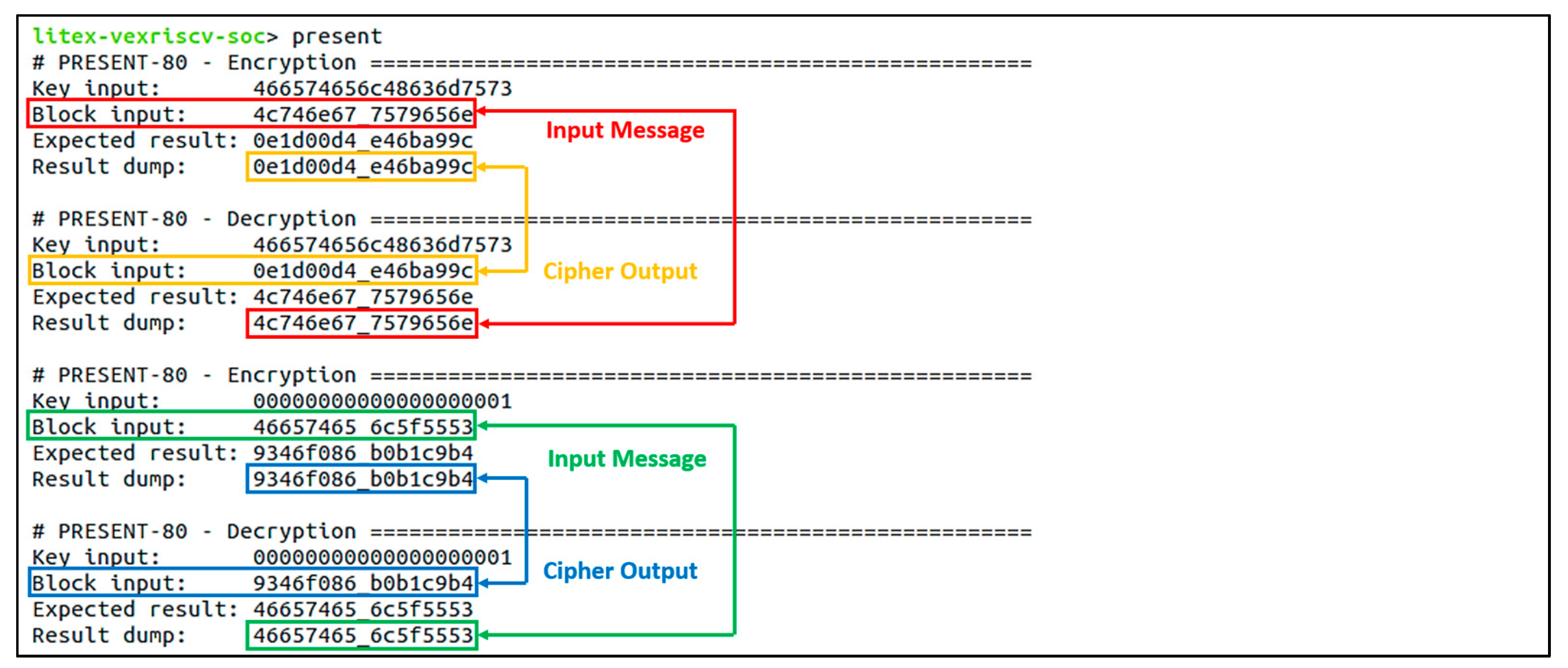
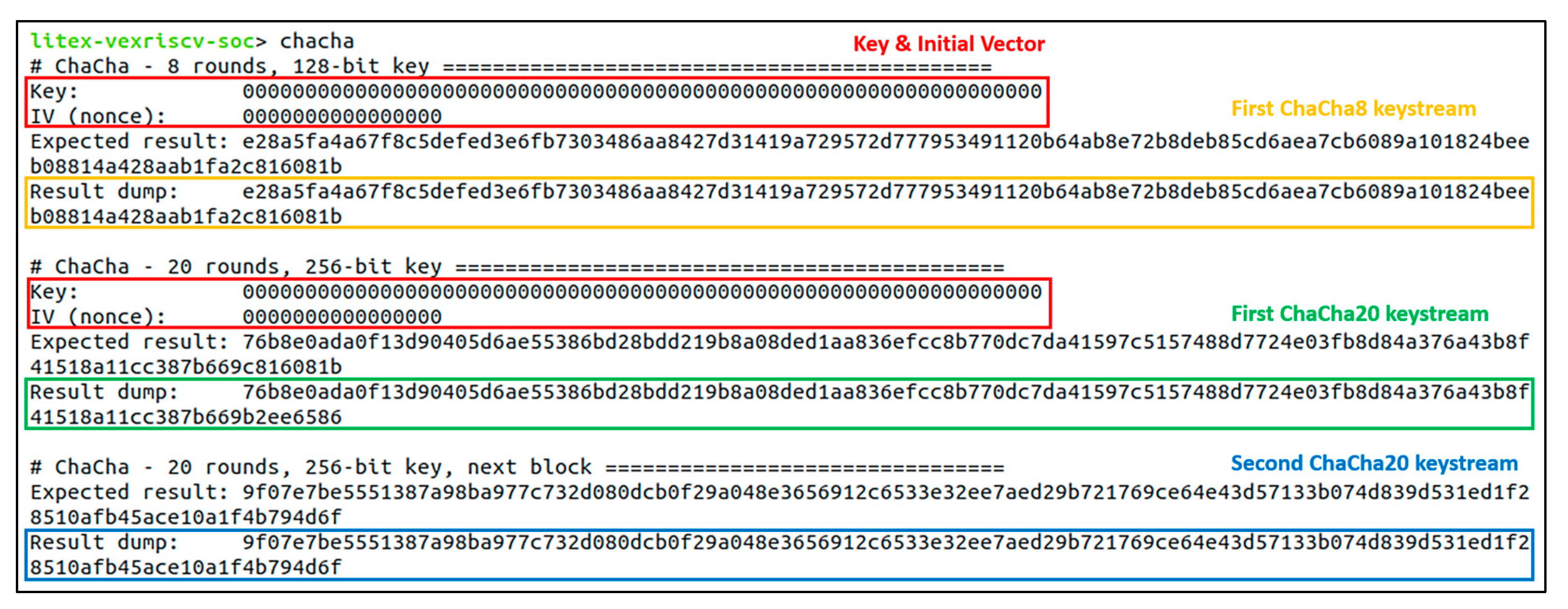
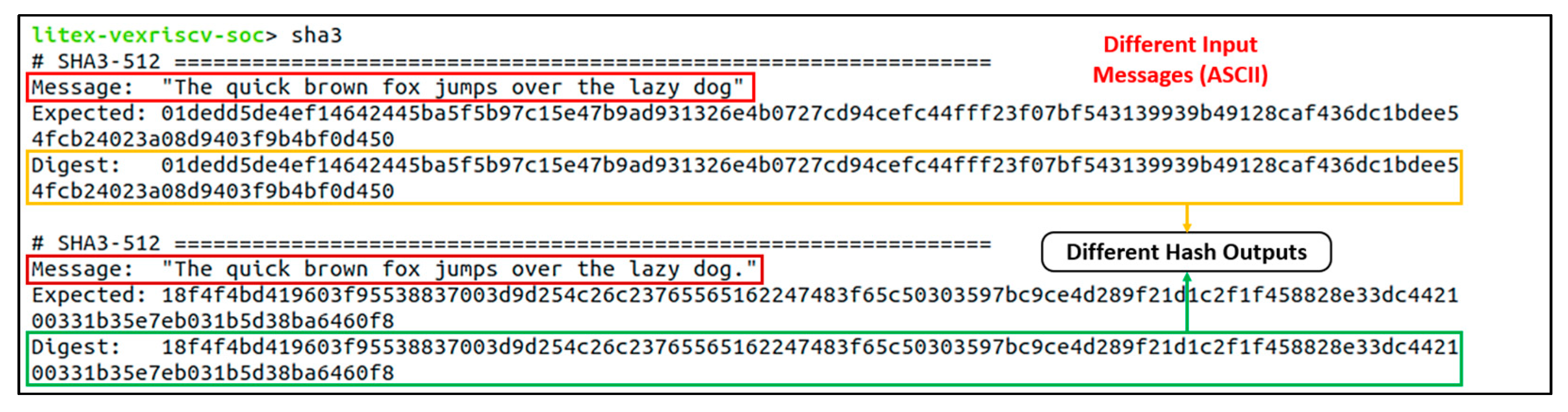
6.2. Accelerator Core Function Verifications
6.3. Cryptographic Processing Speed
7. Evaluations and Discussions
8. Conclusions
Author Contributions
Funding
Institutional Review Board Statement
Informed Consent Statement
Data Availability Statement
Conflicts of Interest
References
- Waterman, A.; Lee, Y.; Patterson, D.A.; Asanovic, K. The RISC-V Instruction Set Manual Volume I: User-Level ISA; EECS Department, University of California: Berkeley, CA, USA, 2016. [Google Scholar]
- Calicchia, L.; Ciotoli, V.; Cardarilli, G.C.; di Nunzio, L.; Fazzolari, R.; Nannarelli, A.; Re, M. Digital Signal Processing Accelerator for RISC-V. In Proceedings of the 26th IEEE International Conference on Electronics, Circuits and Systems (ICECS), Genoa, Italy, 27–29 November 2019; pp. 703–706. [Google Scholar] [CrossRef]
- Zhang, G.; Zhao, K.; Wu, B.; Sun, Y.; Sun, L.; Liang, F. A RISC-V based hardware accelerator designed for Yolo object detection system. In Proceedings of the 2019 IEEE International Conference of Intelligent Applied Systems on Engineering (ICIASE), Fuzhou, China, 26–29 April 2019; pp. 9–11. [Google Scholar] [CrossRef]
- Holler, R.; Haselberger, D.; Ballek, D.; Rossler, P.; Krapfenbauer, M.; Linauer, M. Open-Source RISC-V Processor IP Cores for FPGAs—Overview and Evaluation. In Proceedings of the 2019 8th Mediterranean Conference on Embedded Computing (MECO), Budva, Montenegro, 10–14 June 2019; pp. 1–6. [Google Scholar]
- RISC-V Summit 2022: All Your CPUs Belong to Us. Available online: https://www.eetimes.com/risc-v-summit-2022-all-your-cpus-belong-to-us/ (accessed on 12 May 2023).
- A Winning Processor Portfolio. Available online: https://www.sifive.com/risc-v-core-ip (accessed on 12 May 2023).
- Harris, S.L.; Chaver, D.; Piñuel, L.; Gomez-Perez, J.I.; Liaqat, M.H.; Kakakhel, Z.L.; Kindgren, O.; Owen, R. RVfpga: Using a RISC-V Core Targeted to an FPGA in Computer Architecture Education. In Proceedings of the 2021 31st International Conference on Field-Programmable Logic and Applications (FPL), Dresden, Germany, 30 August–3 September 2021; pp. 145–150. [Google Scholar] [CrossRef]
- Wu, W.; Su, D.; Yuan, B.; Li, Y. Intelligent Security Monitoring System Based on RISC-V SoC. Electronics 2021, 10, 1366. [Google Scholar] [CrossRef]
- Lee, D.; Moon, H.; Oh, S.; Park, D. mIoT: Metamorphic IoT Platform for On-Demand Hardware Replacement in Large-Scaled IoT Applications. Sensors 2020, 20, 3337. [Google Scholar] [CrossRef] [PubMed]
- Zhang, H.; Wu, X.; Du, Y.; Guo, H.; Li, C.; Yuan, Y.; Zhang, M.; Zhang, S. A Heterogeneous RISC-V Processor for Efficient DNN Application in Smart Sensing System. Sensors 2021, 21, 6491. [Google Scholar] [CrossRef] [PubMed]
- Lim, S.-H.; Suh, W.W.; Kim, J.-Y.; Cho, S.-Y. RISC-V Virtual Platform-Based Convolutional Neural Network Accelerator Implemented in SystemC. Electronics 2021, 10, 1514. [Google Scholar] [CrossRef]
- Gamino del Río, I.; Martínez Hellín, A.; Polo, Ó.R.; Jiménez Arribas, M.; Parra, P.; da Silva, A.; Sánchez, J.; Sánchez, S. A RISC-V Processor Design for Transparent Tracing. Electronics 2020, 9, 1873. [Google Scholar] [CrossRef]
- Lee, J.; Chen, H.; Young, J.; Kim, H. RISC-V FPGA Platform Toward ROS-Based Robotics Application. In Proceedings of the 2020 30th International Conference on Field-Programmable Logic and Applications (FPL), Gothenburg, Sweden, 31 August–4 September 2020; p. 370. [Google Scholar] [CrossRef]
- Santos, D.A.; Luza, L.M.; Zeferino, C.A.; Dilillo, L.; Melo, D.R. A Low-Cost Fault-Tolerant RISC-V Processor for Space Systems. In Proceedings of the 2020 15th Design & Technology of Integrated Systems in Nanoscale Era (DTIS), Marrakech, Morocco, 1–3 April 2020; pp. 1–5. [Google Scholar] [CrossRef]
- Andersson, J. Development of a NOEL-V RISC-V SoC Targeting Space Applications. In Proceedings of the 2020 50th Annual IEEE/IFIP International Conference on Dependable Systems and Networks Workshops (DSN-W), Valencia, Spain, 29 June–2 July 2020; pp. 66–67. [Google Scholar] [CrossRef]
- El-hajj, M.; Mousawi, H.; Fadlallah, A. Analysis of Lightweight Cryptographic Algorithms on IoT Hardware Platform. Future Internet 2023, 15, 54. [Google Scholar] [CrossRef]
- Cheng, H.; Großschädl, J.; Marshall, B.; Page, D.; Pham, T. RISC-V Instruction Set Extensions for Lightweight Symmetric Cryptography. TCHES 2022, 2023, 193–237. [Google Scholar] [CrossRef]
- Wei, M.; Yang, G.; Kong, F. Software Implementation and Comparison of ZUC-256, SNOW-V, and AES-256 on RISC-V Platform. In Proceedings of the 2021 IEEE International Conference on Information Communication and Software Engineering (ICICSE), Chengdu, China, 19–21 March 2021; pp. 56–60. [Google Scholar] [CrossRef]
- Marshall, B.; Page, D.; Hung Pham, T. A lightweight ISE for ChaCha on RISC-V. In Proceedings of the 2021 IEEE 32nd International Conference on Application-specific Systems, Architectures and Processors (ASAP), Virtual Conference, 7–9 July 2021; pp. 25–32. [Google Scholar] [CrossRef]
- Marshall, B.; Newell, G.R.; Page, D.; Saarinen, M.-J.O.; Wolf, C. The design of scalar AES Instruction Set Extensions for RISC-V. Cryptol. Eprint Arch. 2020, 1–28. [Google Scholar] [CrossRef]
- Pojoga, G.; Papagiannopoulos, K. Low-Latency Implementation of the GIFT Cipher on RISC-V Architectures. In Proceedings of the 19th ACM International Conference on Computing Frontiers, Turin, Italy, 17–19 May 2022; pp. 287–295. [Google Scholar] [CrossRef]
- Altınay, Ö.; Örs, B. Instruction Extension of RV32I and GCC Back End for Ascon Lightweight Cryptography Algorithm. In Proceedings of the 2021 IEEE International Conference on Omni-Layer Intelligent Systems (COINS), Barcelona, Spain, 23–25 August 2021; pp. 1–6. [Google Scholar] [CrossRef]
- Zheng, X.; Wu, J.; Lin, X.; Gao, H.; Cai, S.; Xiong, X. Hardware/Software Co-design of Cryptographic SoC Based on RISC-V Virtual Prototype. IEEE Trans. Circuits Syst. II Express Briefs, 2023; Early Access. [Google Scholar] [CrossRef]
- Abbas, Y.A.; Jidin, R.; Jamil, N.; Z’aba, M.R.; Rusli, M.E.; Tariq, B. Implementation of PRINCE algorithm in FPGA. In Proceedings of the 6th International Conference on Information Technology and Multimedia (ICMI), Putrajaya, Malaysia, 8–10 December 2014; pp. 1–4. [Google Scholar] [CrossRef]
- Abdullah, A.A.; Obeid, N.R. Efficient Implementation for PRINCE Algorithm in FPGA Based on the BB84 Protocol. J. Phys. Conf. Ser. 2021, 1818, 012216. [Google Scholar] [CrossRef]
- Guo, X.; Chen, Z.; Schaumont, P. Energy and Performance Evaluation of an FPGA-Based SoC Platform with AES and PRESENT Coprocessors. In Embedded Computer Systems: Architectures, Modeling, and Simulation; Bereković, M., Dimopoulos, N., Wong, S., Eds.; Springer: Berlin/Heidelberg, Germany, 2008; Volume 5114, pp. 106–115. [Google Scholar]
- At, N.; Beuchat, J.L.; Okamoto, E.; San, İ.; Yamazaki, T. Compact Hardware Implementations of ChaCha, BLAKE, Threefish, and Skein on FPGA. IEEE Trans. Circuits Syst. I Regul. Pap. 2014, 61, 485–498. [Google Scholar] [CrossRef]
- Sundal, M.; Chaves, R. Efficient FPGA Implementation of the SHA-3 Hash Function. In Proceedings of the 2017 IEEE Computer Society Annual Symposium on VLSI (ISVLSI), Bochum, Germany, 3–5 July 2017; pp. 86–91. [Google Scholar] [CrossRef]
- Bensalem, H.; Blaquière, Y.; Savaria, Y. An efficient OpenCL-Based implementation of a SHA-3 co-processor on an FPGA-centric platform. IEEE Trans. Circuits Syst. II Express Briefs 2022, 70, 1144–1148. [Google Scholar] [CrossRef]
- Nannipieri, P.; Bertolucci, M.; Baldanzi, L.; Crocetti, L.; Di Matteo, S.; Falaschi, F.; Fanucci, L.; Saponara, S. SHA2 and SHA-3 Accelerator Design in a 7 nm Technology within the European Processor Initiative. Microprocess. Microsyst. 2021, 87, 103444. [Google Scholar] [CrossRef]
- Tehrani, E.; Graba, T.; Merabet, A.S.; Danger, J.-L. RISC-V Extension for Lightweight Cryptography. In Proceedings of the 2020 23rd Euromicro Conference on Digital System Design (DSD), Kranj, Slovenia, 26–28 August 2020; pp. 222–228. [Google Scholar] [CrossRef]
- Stoffelen, K. Efficient Cryptography on the RISC-V Architecture. In Progress in Cryptology—LATINCRYPT 2019; Schwabe, P., Thériault, N., Eds.; Springer: Cham, Switzerland, 2019; Volume 11774, pp. 323–340. [Google Scholar]
- RISC-V Foundation. Rocket Chip Generator. 2019. Available online: https://github.com/chipsalliance/rocket-chip (accessed on 7 January 2023).
- Petrisko, D.; Gilani, F.; Wyse, M.; Jung, D.C.; Davidson, S.; Gao, P.; Zhao, C.; Azad, Z.; Canakci, S.; Veluri, B.; et al. BlackParrot: An Agile Open-Source RISC-V Multicore for Accelerator SoCs. IEEE Micro 2020, 40, 93–102. [Google Scholar] [CrossRef]
- Borghoff, J.; Canteaut, A.; Güneysu, T.; Kavun, E.B.; Knezevic, M.; Knudsen, L.R.; Leander, G.; Nikov, V.; Paar, C.; Rechberger, C.; et al. PRINCE—A Low-Latency Block Cipher for Pervasive Computing Applications. In Advances in Cryptology—ASIACRYPT 2012; Wang, X., Sako, K., Eds.; Springer: Berlin/Heidelberg, Germany, 2012; Volume 7658, pp. 208–225. [Google Scholar]
- Bogdanov, A.; Knudsen, L.R.; Leander, G.; Paar, C.; Poschmann, A.; Robshaw, M.J.; Seurin, Y.; Vikkelsoe, C. PRESENT: An ultra-lightweight block cipher. In Cryptographic Hardware and Embedded Systems-CHES 2007: 9th International Workshop, Vienna, Austria, 10–13 September 2007. Proceedings 9; Springer: Berlin/Heidelberg, Germany, 2007; pp. 450–466. [Google Scholar]
- Bernstein, D.J. ChaCha, a variant of Salsa20. In Workshop Record of SASC; The University of Illinois at Chicago: Chicago, IL, USA, 2008; Volume 8, pp. 3–5. [Google Scholar]
- Bernstein, D.J. The Salsa20 family of stream ciphers. In New Stream Cipher Designs; Robshaw, M., Billet, O., Eds.; Springer: Berlin/Heidelberg, Germany, 2008; Volume 4986, pp. 84–97. [Google Scholar]
- Bernstein, D.J. Salsa20 Specification. 2005. Available online: http://www.ecrypt.eu.org/stream/salsa20pf.html (accessed on 24 December 2022).
- Nir, Y.; Langley, A. ChaCha20 and Poly1305 for IETF Protocols. RFC 8439. June 2018. Available online: https://www.rfc-editor.org/rfc/rfc8439 (accessed on 24 December 2022).
- Dworkin, M.J. SHA-3 Standard: Permutation-Based Hash and Extendable-Output Functions. Standard NIST FIPS-202. August 2015. Available online: https://doi.org/10.6028/NIST.FIPS.202 (accessed on 24 December 2022).
- Kavun, E.B.; Yalcin, T. A Lightweight Implementation of Keccak Hash Function for Radio-Frequency Identification Applications. In International Workshop on Radio Frequency Identification: Security and Privacy Issues; Springer: Berlin/Heidelberg, Germany, 2010; pp. 258–269. [Google Scholar]
- OpenCores. SHA3 (KECCAK). Available online: https://opencores.org/projects/sha3 (accessed on 24 December 2022).
- EnjoyDigital. LiteX. Available online: https://github.com/enjoy-digital/litex (accessed on 19 February 2022).
- Saarinen, M.-J.O. Very Small, Readable Implementation of the SHA3 Hash Function. Available online: https://github.com/mjosaarinen/tiny_sha3 (accessed on 24 December 2022).


| Name | Address | Description |
|---|---|---|
| Key Input | 0x10–0x13 | 128-bit key input registers |
| Block Input | 0x20–0x21 | 64-bit message input registers |
| Result | 0x30–0x31 | 64-bit cipher output registers |
| Control | 0x08 | Accelerator control bit |
| Status | 0x09 | Accelerator status bit |
| Configuration | 0x0A | Accelerator configuration bit |
| Name | Address | Description |
|---|---|---|
| Configuration | 0x00 | Configuration of encryption or decryption |
| Key Input | 0x01–0x03 | 80-bit key input register |
| Data Input | 0x04–0x05 | 64-bit data input register |
| Cipher Output | 0x06–0x07 | 64-bit cipher output register |
| Name | Address | Description |
|---|---|---|
| Key Input | 0x10–0x17 | 256-bit key input registers |
| Nonce Input | 0x20–0x21 | 64-bit number-use-once registers |
| Data Input | 0x40–0x4F | Optional 512-bit message input registers |
| Data Output | 0x80–0x8F | 512-bit keystream output registers |
| Control | 0x08 | Accelerator control bit |
| Status | 0x09 | Accelerator status bit |
| Configuration | 0x30 | Accelerator configuration bit |
| Name | Address | Description |
|---|---|---|
| Reset | 0x00 | Set and reset input |
| Input | 0x01 | 32-bit input register |
| Byte Number | 0x02 | Set index of last byte |
| Input Last | 0x03 | Set the last input and start |
| Status | 0x09 | Accelerator status bit |
| Hash Output | 0x10–0x1F | 512-bit hash output registers |
| Top Design * | VexRiscv | PRINCE | PRESENT-80 | ChaCha | SHA3-512 | |
|---|---|---|---|---|---|---|
| LUTs | 11,830 | 2025 | 1561 | 489 | 2890 | 3003 |
| Logic LUTs | 11,684 | 2025 | 1561 | 489 | 2890 | 3003 |
| LUTs as RAMs | 144 | 0 | 0 | 0 | 0 | 0 |
| SRLs | 2 | 0 | 0 | 0 | 0 | 0 |
| FFs | 9552 | 1279 | 648 | 901 | 1960 | 2291 |
| RAMB | 36 | 9 | 0 | 0 | 0 | 0 |
| DSP | 4 | 4 | 0 | 0 | 0 | 0 |
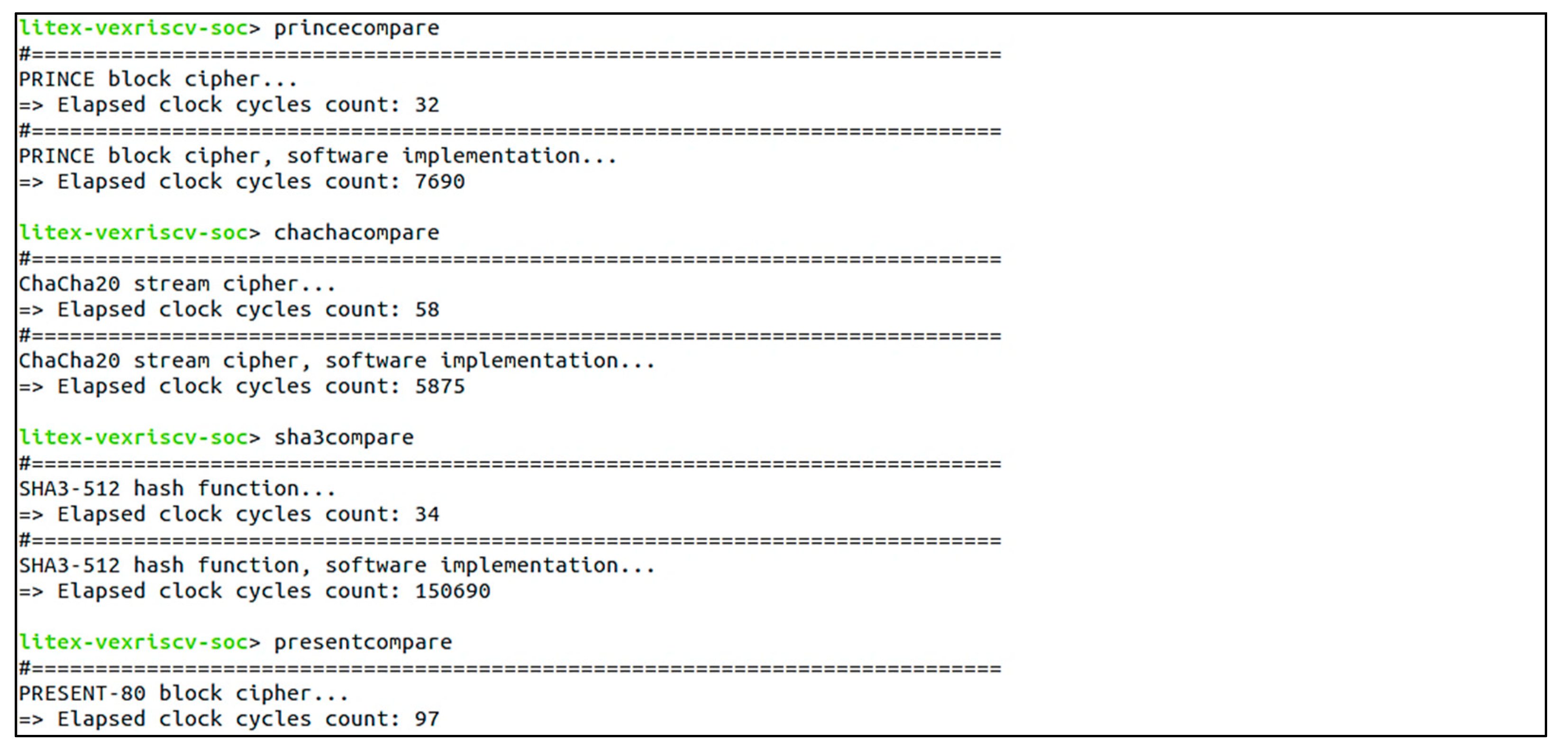
| Hardware | Software | Gains | |
|---|---|---|---|
| PRINCE | 32 cycles | 7682 cycles | 240 |
| PRESENT-80 | 97 cycles | - | - |
| ChaCha20 | 58 cycles | 5876 cycles | 101 |
| SHA3-512 | 34 cycles | 150,693 cycles * | 4432 |
| Algorithm | Output Size (Bit) | Device | Max. Frequency (MHz) | Throughput (Mbps) | Slices | Block RAM | Power (Watts) |
|---|---|---|---|---|---|---|---|
| PRINCE on SoC | 64 | Artix-7 XC7A100T | 75 1 | 149 | 392 | 0 | 0.054 4 |
| PRINCE [24] | 64 | Virtex-4 FF668 | 31.765 | 2032 | 956 | - | 0.165 |
| PRINCE-BB84 [25] | 64 | Kintex-7 | 61.42 | 3931 | 539 | - | 0.045 |
| PRESENT-80 on SoC | 64 | Artix-7 XC7A100T | 75 1 | 49 | 123 | 0 | 0.003 4 |
| PRESENT-80 [26] | 64 | Spartan-3E | 50 | 6.25 2 | 460 | - | 0.044 |
| ChaCha20 on SoC | 512 | Artix-7 XC7A100T | 75 1 | 662 | 723 | 0 | 0.008 4 |
| ChaCha20 [27] | 512 | Virtex-6 XC6VLX75T | 345 | 254 | 77 | 2 | - |
| SHA3-512 on SoC | 512 | Artix-7 XC7A100T | 75 1 | 1129 | 750 | 0 | 0.211 4 |
| SHA3-512 [28] | 512 | Virtex-5 | 223 | 5350 | 1192 | - | - |
| SHA3-512 [29] | 512 | Arria 10 | 312 | 22,360 | 149,500 | 787 | - |
| SHA3-512 [30] | 512 | ASIC—TSMC 7nm | 5100 | 115,200 | 30,740 3 | - | 0.025 |
| This Work | [31] | [32] | [26] | |
|---|---|---|---|---|
| Device | Artix-7 XC7A100T | Artix-7 XC7A100T | FE310-G000 SoC | Spartan-3E |
| Processor core | VexRiscv | VexRiscv | SiFive E31 | MicroBlaze |
| Operation frequency | 75 MHz | - | - | 50 MHz |
| Implementation type | SoC Accelerator | HW instructions | SW instructions | SoC accelerator |
| Algorithm performance (cycles) | ||||
| PRINCE | 31 | 35 1 | - | - |
| ChaCha20 | 58 | - | 1787 2 | - |
| SHA3-512 (Keccak) | 34 | - | 13,774 | - |
| PRESENT-80 | 97 | 160 1 | - | 514 3 |
Disclaimer/Publisher’s Note: The statements, opinions and data contained in all publications are solely those of the individual author(s) and contributor(s) and not of MDPI and/or the editor(s). MDPI and/or the editor(s) disclaim responsibility for any injury to people or property resulting from any ideas, methods, instructions or products referred to in the content. |
© 2023 by the authors. Licensee MDPI, Basel, Switzerland. This article is an open access article distributed under the terms and conditions of the Creative Commons Attribution (CC BY) license (https://creativecommons.org/licenses/by/4.0/).
Share and Cite
Ma, K.-M.; Le, D.-H.; Pham, C.-K.; Hoang, T.-T. Design of an SoC Based on 32-Bit RISC-V Processor with Low-Latency Lightweight Cryptographic Cores in FPGA. Future Internet 2023, 15, 186. https://doi.org/10.3390/fi15050186
Ma K-M, Le D-H, Pham C-K, Hoang T-T. Design of an SoC Based on 32-Bit RISC-V Processor with Low-Latency Lightweight Cryptographic Cores in FPGA. Future Internet. 2023; 15(5):186. https://doi.org/10.3390/fi15050186
Chicago/Turabian StyleMa, Khai-Minh, Duc-Hung Le, Cong-Kha Pham, and Trong-Thuc Hoang. 2023. "Design of an SoC Based on 32-Bit RISC-V Processor with Low-Latency Lightweight Cryptographic Cores in FPGA" Future Internet 15, no. 5: 186. https://doi.org/10.3390/fi15050186
APA StyleMa, K.-M., Le, D.-H., Pham, C.-K., & Hoang, T.-T. (2023). Design of an SoC Based on 32-Bit RISC-V Processor with Low-Latency Lightweight Cryptographic Cores in FPGA. Future Internet, 15(5), 186. https://doi.org/10.3390/fi15050186