Abstract
Object detection is an important task for many applications, like transportation, security, and medical applications. Many of these applications are needed on edge devices to make local decisions. Therefore, it is necessary to provide low-cost, fast solutions for object detection. This work proposes a configurable hardware core on a field-programmable gate array (FPGA) for object detection. The configurability of the core allows its deployment on target devices with diverse hardware resources. The object detection accelerator is based on YOLO, for its good accuracy at moderate computational complexity. The solution was applied to the design of a core to accelerate the Tiny-YOLOv3, based on a CNN developed for constrained environments. However, it can be applied to other YOLO versions. The core was integrated into a full system-on-chip solution and tested with the COCO dataset. It achieved a performance from 7 to 14 FPS in a low-cost ZYNQ7020 FPGA, depending on the quantization, with an accuracy reduction from 2.1 to 1.4 points of .
1. Introduction
Object detection [1,2] determines if an object is present in an image. This capacity to automatically detect objects has a wide range of applications, like transportation, medical, and security applications [3,4]. For example, in smart cities, traffic analysis from images determines the number of cars, persons, etc. and takes decisions to improve traffic and public transport. Decisions made locally near the scenario under analysis are more efficient [5]. Therefore, it is important to provide edge Internet-of-Things (IoT) devices with the capacity to run complex machine learning algorithms, in particular, object detection.
The recent development of deep learning and in particular the convolutional neural network (CNN) had a major contribution to the recent improvement of the accuracy of object detectors, compared to other traditional machine learning algorithms [6]. The recent state-of-the-art object detectors are all based on CNNs, which can automatically learn complex features that are used to detect and classify objects.
There are two approaches to design object detectors using CNNs [1,7]. The two-stage object detector follows the traditional algorithm where it first finds regions of interest and identifies them as candidate bounding boxes. It then classifies each candidate bounding box in a second stage. Well-known two-stage detectors are R-CNN [8], fast R-CNN [9], R-FCN [10], faster R-CNN [11], and mask R-CNN [12]. A second approach to object detection considers a single phase only. These algorithms integrate both regression and classification in a single step. Common one-stage detectors are YOLO [13] with its different versions: YOLOv2 [14], YOLOv3 [15], and YOLOv4 [16] and RetinaNet [17].
The best object detector for a particular application depends on the target requirements in terms of speed and detection precision. Two-stage object detectors are more precise than one-stage detectors but are computationally more demanding [18]. Therefore, in a distributed edge computing scenario the one-stage detectors are the preferred choice for their lower cost with good accuracy.
Even the one-stage detectors require high computing power to achieve real-time performance [18]. For this reason, graphics processing units (GPUs) are generally used to deploy CNNs due to their high-performance floating-point computing. However, GPUs are power-hungry and cannot be deployed in edge devices with reduced energy [19]. Dedicated hardware solutions are therefore important for the successful deployment of CNN-based object detectors on edge devices [19]. Many recent works use field-programmable gate arrays (FPGAs) since they offer high computing power with high energy efficiency [20]. Besides, they also offer hardware flexibility, permitting a custom design for particular constraints of the system target.
In this study, we proposed a configurable hardware core for object detection based on YOLO. To improve the performance of the core for object detection, the YOLO algorithm was first quantized from a floating point to a fixed point with a small precision drop in the mean average precision (mAP).
The system was tested with Tiny-YOLOv3, a lightweight version of YOLOv3 [15]. The core was integrated into a full system-on-chip (SoC) and prototyped in a low-cost ZYNQ7020 FPGA. The solution with 16-bit quantization achieved 7 frames per second for 416 × 416 sized images in the ZYNQ7020 with 31.5 . The 8-bit quantization solution doubled the throughput but reduced the by 0.7 percentage points.
The article is organized as follows. Section 2 introduces the background of CNNs and object detection with YOLO. Section 3 describes the architecture of the object detector accelerator. Section 4 describes the mapping process of Tiny-YOLOv3 on the proposed architecture. Section 5 presents the results of the solution for the two fixed-point representations and compares the proposed system with other computing platforms and other FPGA-based object detector works. Finally, Section 6 concludes the article.
2. Background and Related Work
2.1. Convolutional Neural Networks
CNNs are mainly composed of convolutional layers. Other commonly found layers in CNNs are pooling, batch-normalize, shortcut, routing, and upsample layers.
The input of convolutional layers is divided into C channels, where each channel is defined as a () feature map (FM). Each kernel used in the convolution has C channels. The number of output channels N is the same as the number of kernels used. Each value on the output is the accumulation of the products of the input with the overlapped kernel.
CNNs use pooling layers to reduce the size of the FMs. The most common pooling operations divide the feature map into regions and select either the larger (max-pooling) or the average (average-pooling) value.
Batch-normalize layers set the average of the input values to zero and the standard deviation to one. After that, the values are scaled and shifted using the (,) parameters also learned during training. This control of the input distribution speeds up training and improves accuracy. For a given value y, the normalization outputs
where is the average, is the standard deviation, is the scale, and is the batch normalization bias. The additional term is used to avoid numerical errors related with denominators too close to zero.
A shortcut layer skips one or more layers by adding an output feature map of a previous layer to a current layer. Routing and upsampling layers are usually associated with objection detection [15]. The routing layer concatenates outputs from different layers creating stacked separate output channels. The upsampling layer increases the size (width and height) of a feature map to detect objects at different scales and obtain more information from features identified in the input map. The simplest upsample method consists in repeating each value in an feature map four times in a square.
Many CNN models have been proposed since the success of AlexNet [20], VGG-16 [20], and GoogLeNet [20] for image classification. These CNN networks differ mainly in the number and sequence of layers and the number and size of kernels. Compared to the first two CNN models, GoogLeNet introduced parallel convolutions applied to the same input feature map (IFM), followed by concatenation. It basically allows processing the inputs at multiple scales. Deeper and larger CNN models have followed and improved accuracy at the cost of increased computational complexity. ResNet [20] is a deeper network compared to its predecessors. The network model introduces for the first time the shortcut layers to avoid the vanishing gradient problem observed during backpropagation.
Some CNN models were specifically designed for object detection. Darknet-53 [15] is the base model of YOLOv3 that employs shortcut layers to allow a deeper network. Darknet-53 is the backbone model of the YOLOv3 object detector. In general, YOLO models have lightweight versions. A few lightweight versions were proposed for YOLOv3 like Tiny = YOLOv3 based on Tiny-Darnet-53, with a reduced number of weights (from 62 to 8.8 million parameters) and computations (from 33 to 2.8 GOPS) compared to the full model.
2.2. Tiny YOLOv3
Object detectors locate and classify objects present in an image. Typically, the detectors locate objects and draw a bounding box around it and then classify the objects as belonging to a predefined set of classes.
YOLO and all its versions [21] are one-stage object detectors with a common model topology based on convolutional neural networks. YOLOv3 has three different versions for different image sizes: 320 × 320, 416 × 416, or 608 × 608. The YOLO detector extracts features using a CNN and returns candidate bounding boxes from those features for three different scales: 52 × 52, 26 × 26, and 13 × 13. The set of candidate bounding boxes are filtered based on a score that depends on each class. Multiple detections of the same object are then removed using non-maximum suppression. The final bounding box and the classification of each object are presented over the original image.
The CNN model of YOLO has convolutional, shortcut, YOLO, upsample, and route layers. The YOLO layer is specific for this type of detector. It applies the logistic activation to the predictions of each bounding box. Max-pooling is not used in YOLO. Instead, it considers convolutional layers with stride two. Batch-normalization is applied to all convolutional layers, and all layers use the Leaky ReLU activation function, except the layers before YOLO layers that uses a linear activation function. YOLO is able to detect objects of different sizes using three different scales: 52 × 52 to detect small objects, 26 × 26 to detect medium objects, and 13 × 13 to detect large objects. Consequently, multiple bounding boxes of the same object might be found. To reduce multiple detections of an object to a single one, the non-maximum suppression algorithm is used [22].
The work proposed in this article targets tiny versions of YOLO that replace convolutions with a stride of two by convolutions with max-pooling and does not use shortcut layers. Tests were made with Tiny-YOLOv3 (see Figure 1).
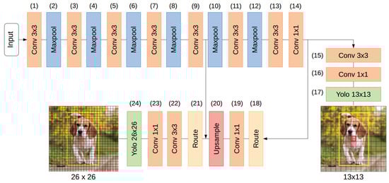
Figure 1.
Tiny YOLOv3 layer diagram.
Table 1 details the sequence of layers with regards to the input, output, and kernel sizes and the activation function used in each convolutional layer. Most of the convolutional layers perform feature extraction. This network uses pooling layers to reduce the feature map resolution.

Table 1.
Tiny-YOLOv3 layers.
This network uses two cell grid scales: () and (). The indicated resolutions are specific to the tiny YOLOv3-416 version.
The first part of the network is composed of a series of convolutional and maxpool layers. Maxpool layers reduce the FMs by a factor of four along the way. Note that layer 12 performs pooling with stride 1, so the input and output resolution is the same. In this network implementation, the convolutions use zero padding around the input FMs, so the size is maintained in the output FMs. This part of the network is responsible for the feature extraction from the input image.
The object detection and classification part of the network performs object detection and classification at () and () grid scales.
The detection at a lower resolution is obtained by passing the feature extraction output over and convolutional layers and a YOLO layer at the end.
The detection at the higher resolution follows the same procedure but uses FMs from two layers of the network. The second detection uses intermediate results from the feature extraction layers concatenated with upscaled FMs used for the lower resolution detection.
The combination of FMs from two different resolutions contributes to more meaningfulness using the information from the upsampled layer and the finer-grained information from the earlier feature maps [15].
2.3. CNN Model Optimization
The CNN execution can be accelerated by approximating the computation at the cost of minimal accuracy drop. One of the most common strategies is reducing the precision of operations. During training, the data are typically in single-precision floating-point format. For inference in FPGAs, the feature maps and kernels are usually converted to fixed-point format with less precision, typically 8 or 16 bits, reducing the storage requirements, hardware utilization, and power consumption [23].
Quantization is done by reducing the operand bit size. This restricts the operand resolution, affecting the resolution of the computation result. Furthermore, representing the operands in fixed-point instead of floating-point translates into another reduction in terms of required resources for computation.
The simplest quantization method consists of setting all weights and inputs to the same format across all layers of the network. This is referred to as static fixed-point (SFP). However, the intermediate values still need to be bit-wider to prevent further accuracy loss.
In deep networks, there is a significant variety of data ranges across the layers. The inputs tend to have larger values at later layers, while the weights for the same layers are smaller in comparison. The wide range of values makes the SFP approach not viable since the bit width needs to expand to accommodate all values.
This problem is addressed by dynamic fixed-point (DFP), which consists of the attribution of different scaling factors to the inputs, weights, and outputs of each layer.
Table 2 presents an accuracy comparison between floating-point and DFP implementations for two known neural networks. The fixed-point precision representation led to an accuracy loss of less than 1%.
Table 2.
Accuracy comparison with the ImageNet dataset, adapted from [24].
Quantization can also be applied to the CNN used in YOLO or another object detector model. The accuracy drop caused by the conversion to fixed-point of Tiny-YOLOv3 was determined for the MS COCO 2017 test dataset. The results show that a 16-bit fixed-point model presented a drop below 1.4 compared to the original floating-point model and 2.1 for 8-bit quantization.
Batch-normalization folding [27] is another important optimization method that folds the parameters of the batch-normalization layer into the preceding convolutional layer. This reduces the number of parameters and operations of the model. The method updates the pre-trained floating-point weights w and biases b to and according to Equation (2) before applying quantization.
2.4. Convolutional Neural Network Accelerators in FPGA
One of the advantages of using FPGAs is the capacity to design parallel architectures that explore the available parallelism of the algorithm. CNN models have many levels of parallelism to explore [28]:
- intra-convolution: multiplications in 2D convolutions are implemented concurrently;
- inter-convolution: multiple 2D convolutions are computed concurrently;
- intra-FM: multiple pixels of a single output FM are processed concurrently;
- inter-FM: multiple output FM are processed concurrently.
Different implementations explore some or all these forms of parallelism [29,30,31,32,33] and different memory hierarchies to buffer data on-chip to reduce external memory accesses.
Recent accelerators, like [33], have on-chip buffers to store feature maps and weights. Data access and computation are executed in parallel so that a continuous stream of data is fed into configurable cores that execute the basic multiply and accumulate (MAC) operations. For devices with limited on-chip memory, the output feature maps (OFM) are sent to external memory and retrieved later for the next layer. High throughput is achieved with a pipelined implementation.
Loop tiling is used if the input data in deep CNNs are too large to fit in the on-chip memory at the same time [34]. Loop tiling divides the data into blocks placed in the on-chip memory. The main goal of this technique is to assign the tile size in a way that leverages the data locality of the convolution and minimizes the data transfers from and to external memory. Ideally, each input and weight is only transferred once from external memory to the on-chip buffers. The tiling factors set the lower bound for the size of the on-chip buffer.
A few CNN accelerators have been proposed in the context of YOLO. Wei et al. [35] proposed an FPGA-based architecture for the acceleration of Tiny-YOLOv2. The hardware module implemented in a ZYNQ7035 achieved a performance of 19 frames per second (FPS). Liu et al. [36] also proposed an accelerator of Tiny-YOLOv2 with a 16-bit fixed-point quantization. The system achieved 69 FPS in an Arria 10 GX1150 FPGA. In [37], a hybrid solution with a CNN and a support vector machine was implemented in a Zynq XCZU9EG FPGA device. With a 1.5-pp accuracy drop, it processed 40 FPS.
A hardware accelerator for the Tiny-YOLOv3 was proposed by Oh et al. [38] and implemented in a Zynq XCZU9EG. The weights and activations were quantized with an 8-bit fixed-point format. The authors reported a throughput of 104 FPS, but the precision was about 15% lower compared to a model with a floating-point format. Yu et al. [39] also proposed a hardware accelerator of Tiny-YOLOv3 layers. Data were quantized with 16 bits with a consequent reduction in of 2.5 pp. The system achieved 2 FPS in a ZYNQ7020. The solution does not apply to real-time applications but provides a YOLO solution in a low-cost FPGA. Recently, another implementation of Tiny-YOLOv3 [40] with a 16-bit fixed-point format achieved 32 FPS in a UltraScale XCKU040 FPGA. The accelerator runs the CNN and pre- and post-processing tasks with the same architecture. Recently, another hardware/software architecture [41] was proposed to execute the Tiny-YOLOv3 in FPGA. The solution targets high-density FPGAs with high utilization of DSPs and LUTs. The work only reports the peak performance.
This study proposes a configurable hardware core for the execution of object detectors based on Tiny-YOLOv3. Contrary to almost all previous solutions for Tiny-YOLOv3 that target high-density FPGAs, one of the objectives of the proposed work was to target low-cost FPGA devices. The main challenge of deploying CNNs on low-density FPGAs is the scarce on-chip memory resources. Therefore, we cannot assume ping-pong memories in all cases, enough on-chip memory storage for full feature maps, nor enough buffer for the full output map. Previous works on high-density FPGAs assumed enough on-chip memory to implement weight memory ping-pong and to store full feature maps and therefore cannot be mapped on low-density FPGAs.
The work proposed in this article modifies the architecture designed in [40] so that it can be mapped to low-density FPGAs. New addressing mechanisms to support feature map tilling, optimization of cores to improve DSP utilization, and multiple DMAs to take advantage of multiple memory controller ports were the main hardware modifications.
3. Hardware Core for Object Detection with YOLO
Figure 2 presents the detailed architecture of the proposed core for the execution of the CNN base network of tiny versions of YOLO.
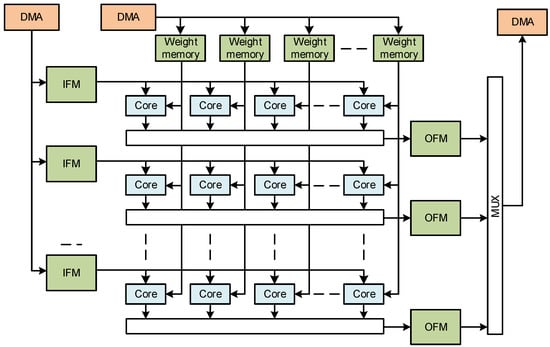
Figure 2.
Block diagram of the proposed accelerator of the CNN network of Tiny-YOLO.
The architecture uses direct memory access (DMA) to read and write data from the main external memory. Bypassing the CPU for the memory accesses frees the CPU to execute other tasks during data transfers.
The data from the main memory are stored in distributed on-chip memories. There are three sets of memories in the architecture: one for input feature maps, one for output feature maps, and another for weight kernels and biases. The memories include a set of address generators that send data in a particular order to the cores to be processed.
The computing cores are organized in a two-dimensional matrix to enable intra- and inter-parallelism, as discussed in Section 2.4. Cores in the same line receive the same input feature map but different kernels. Cores in the same column receive the same kernels but different input feature maps.
The results from each core line are written into output memory buffers and then transferred back into main memory through the DMA.
The dataflow of the accelerator is divided into three phases: memory read, compute, and memory write, as is presented in Figure 3.
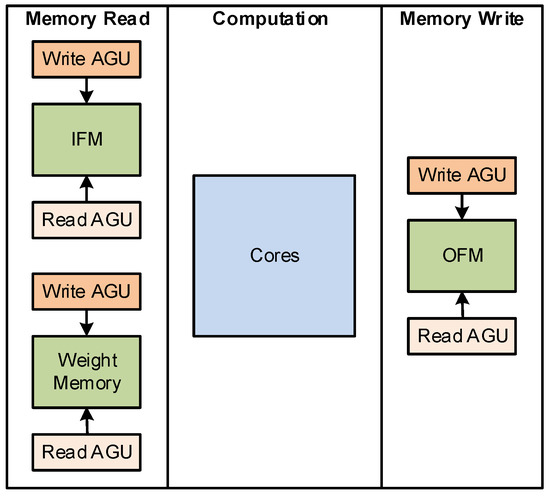
Figure 3.
Dataflow execution of the accelerator.
In the memory read phase, the data are transferred from the main memory to the IFM memories. In this phase, the read operations from the main memory and the writes to the memories are controlled by external address generator units (AGUs).
The compute phase sends the IFM and the weights from on-chip memories for computation, computes the layers in the custom cores, and writes the result in the OFM memories. In this phase, all the internal AGUs control the reads from the IFM memories, the operations at the cores, and the writes to the OFM memories.
In the memory write part, the data from the OFM memories are transferred back to the main memory. An external AGU controls the read accesses to the OFM memories and the write transfers to the main memory.
This architecture allows the pipelining of consecutive dataflows. The execution of a second dataflow starts after the memory read phase of the first dataflow is completed. At this point, the accelerator executes the memory read phase of the second dataflow and the compute phase of the first dataflow simultaneously.
3.1. Address Generator
The on-chip memories are controlled by AGUs. Each group of memories is controlled by a pair of AGU groups: one for the external accesses and another for the internal accesses. All the cores for computation also use a AGU to generate control signals.
An address generator unit can access the memories in a nested loop pattern, which is described by Algorithm 1.
| Algorithm 1 Address generator pattern. |
|
A duty input sets the number of period cycles for which the address is incremented. So, if and , the address is only incremented in two of the three period cycles. A delay input sets an initial latency of clock cycles between enabling run and actually starting the address generation.
The start, iterations, period, incr, and shift signals are configured via software.
A pattern with more nested loops is achieved by chaining multiple AGUs. Each additional chained address generator unit adds a set of iter, period, shift, and incr configurations.
The AGU for the internal access of the IFMs memories uses three chained simple AGUs since the access pattern required for the convolution has six nested loops.
The external address generation also requires the offset and ping-pong configurations. The offset is the address space between each starting address to read or write from/to the main memory. The ping-pong enables the buffers to work as two independent halves: one half is used in a phase to read and the other to write. They switch in the next phase execution.
3.2. Architecture of the Computing Core Unit
Each computing core receives as input the feature map values, biases, and weights from the on-chip memories. The core outputs the computation result to an OFM memory. The core can be configured to compute multiple IFM channels in parallel using multiple MACs (nMAC parameter). This parallelism requires multiple words of IFM data and kernel weights.
The core supports multiple functions that can be selected during runtime. This runtime configuration allows the acceleration of multiple types of layers.
The convolution function takes the outputs of the several MAC blocks and adds them together. The result of the convolution can be used as-is or be subject to either leaky or sigmoid non-linear activation. The non-linear activations are implemented for the fixed-point format. The core shifts the final result according to the quantization format being used. For the convolution and maxpool function, each computed convolutional result is compared to the previous convolution results of the same maxpool region. The maxpool function can be used in standalone mode using directly one of the words from the IFM data.
To exemplify the versatility of the core, the configurability of the core to run the Tiny-YOLOv3 layers presented in Table 1 is presented in Table 3.
Table 3.
Custom core configurations for Tiny-YOLOv3 layers.
The layers 1 to 8 can be computed in convolutional + maxpool pairs. These layers disable the convolution bypassing and activate the maxpooling. All convolutional layers have leaky activation.
The layers 10 and 12 are maxpool only. These layers bypass the convolution, ignoring all convolution specific configurations.
The 16–17 and 23–24 layers are convolutional + YOLO pairs. These layers can be computed together since the convolution has linear activation, and the YOLO layer consists in performing sigmoid activation to the input feature maps. So, these two layer types can be combined into a convolution with sigmoid activation. Note that only part of the YOLO layer output channels is activated.
The remaining layers perform convolution with leaky activation. All convolutional layers in the neural network use bias.
The custom computational core is controlled by an AGU. The AGU period controls the number of operations required to obtain one result. For example, a maxpool requires a period of , while a convolution with a kernel takes a period. Note the division since nMAC input channels are computed in parallel. The number of final outputs for a phase execution is defined by the iterations of the address generator.
3.3. Configuration Parameters of the Accelerator
Table 4 presents the configuration parameters of the accelerator.
Table 4.
Configuration parameters of the object detector accelerator.
The number of weight memories for kernels used in the design is defined by the nCols parameter. The number of IFM memories used for the input feature maps is defined by the nRows parameter. The number of cores of the computing array is .
The nMACs parameter defines the number of MACs in each core.
The DDR_ADDR_W parameter sets the main memory address width.The DATAPATH_W parameter determines the data width used for computation input and output.
The parameters MEM_BIAS_ADDR_W, MEM_WEIGHT_ADDR_W, MEM_TILE_ADDR_W, and MEM_ADDR_W define the dimensions for the bias, weight, and the IFM and OFM memories, respectively.
3.4. Software API
The proposed accelerator has a C++ API that enables runtime configuration by a CPU. The main class CODCore has an attribute for the memory base address of the core in the system. Besides the constructor, the class has the run(), done(), and clear() methods. The run() method signals the execution of a dataflow phase in the accelerator. The done() checks for a run() completion. The clear() method resets all configurations.
The main class contains three objects, each from a different class. Each class contains methods to configure specific cores in the architecture. The CDma class has methods for the DMA configurations. The CRead class has methods for the AGUs associated with the weights and biases memories. The CComp class contains objects from classes that in turn control the AGUs associated with the IFM memories, custom computing cores, and OFM memories. The custom core configurations are also configured with methods from this class.
4. Running Tiny-YOLOv3 in the Accelerator
This section details the development of the Tiny-YOLOv3 application to execute efficiently on the proposed architecture.
4.1. Storage Data Format
The data storage format implemented in the embedded software influences the loops for convolution. To reduce the number of loops for data access during convolution, the data are stored in memory in a ZXY format instead of the original XYZ format. Figure 4 presents a scheme of both formats for a input feature map.
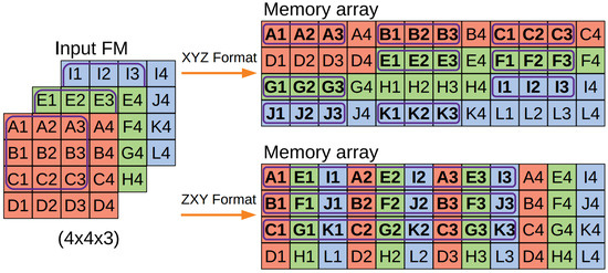
Figure 4.
Data storage formats.
The XYZ format stores the values by column and row of each feature map. In ZXY format, the data are stored by channel first. Figure 4 also highlights the values used to compute the first pixel of a convolution output. The XYZ format disperses the input values in nine groups of three contiguous values. This format requires three loops to iterate across all values: one loop to iterate across the values in each FM row, one loop to iterate across the rows of an FM, and one to iterate across different FMs. The ZXY format stores the input values in three groups of nine contiguous values each. This format requires two loops to access all values: one loop to iterate across all rows and one loop to iterate, in each row, across all values and channels.
4.2. CNN Acceleration
The first eight layers of the network can be executed in convolutional+maxpool layer pairs. To minimize data transfers, each IFM tile is read from the main memory once, and the corresponding OFM tile is computed for all kernels. With this strategy, all the kernels are loaded from memory for the same set of IFM tiles.
Most configurations stay the same across the complete convolutional and maxpool layers execution. The common configurations are set at the start of the function. Note that all the dataflow phases are configured. The variable configurations are mostly related to updating the data pointers for reading and writing data to/from main memory.
The limitations of the on-chip memory buffers require the use of tiling for the IFMs. Figure 5 presents a diagram of the tiling strategy used for the application.
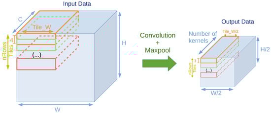
Figure 5.
Data tiling diagram.
The tiling implemented divides the IFM into blocks of four rows, , columns and C channels. The two extra columns per tile are used as padding to maintain the pattern for convolution on the tile edges. The padded columns are not represented in Figure 5 for readability purposes. Since there are nRows memories to store IFM tiles, the same amount of IFM tiles are transferred from the main memory.
With the data in ZXY format, each DMA burst reads contiguous values. Each IFM tile starts two rows after the start of the previous tile. After each DMA burst, the shift configuration updates the pointer to the main memory from the end of the tile row to the start of the next tile row. The memory for IFM tiles operates whenever possible in a ping-pong fashion: the half of the OFM memory used to write data from the main memory toggles between two consecutive datapath phase executions.
The memory for weights is read in sequence. The kernels are read times, one per each convolution done over an IFM tile. After each convolution, the internal AGU points back to the initial address.
The starting address both for reading weights and biases memories is updated according to each set of kernels being used for convolution.
The IFM tile configurations for the Compute phase are constant since the accelerator only operates over one set of IFM tiles at a time. The internal AGU that controls the memory accesses is configured to generate a five-loop pattern.
The inner-most loop iterates over the values in the same row across all channels for a total of . Like the memories for weights, the memories for IFM values output nMACs values in the same word. The execution of these two loops performs a single convolution.
The third and fourth loops generate the pattern for the maxpool. The third loop offsets the address to perform the convolution in the next column ( addresses added). The fourth loop offsets the address to start in the next row (adding to the address) and one column to the left (subtracting ).
The fifth loop generates the pattern to move across the output squares of the IFM tile by adding offsetting the address two columns () to the left.
The custom core takes iterations for each convolution, for a total of convolutions per IFM tile. The convolution result and bias values are shifted to comply with the DFP quantization.
The remaining convolutional layers of Tiny-YOLOv3 are accelerated in isolation (only the convolutional layer) or combined with a YOLO or upsample layer.
Figure 6 presents the tiling format for the remaining convolutional layers. After layer 8, the IFMs are either or and therefore .
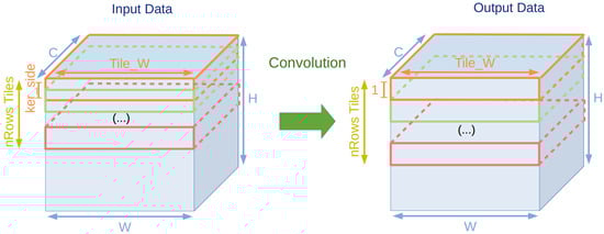
Figure 6.
Data tiling diagram after layer 8.
The main difference in configurations happens for the memories of the IFM tiles in the memory read phase.
The convolutional layers 16 and 23 are paired and executed with the YOLO layers 17 and 24, respectively, in the same datapath configuration. The convolutional layers 16 and 23 have linear activation and the YOLO layer operations are equivalent to performing sigmoid activation to selected input channels. Combining both layers consists of performing a regular convolutional layer with sigmoid activation.
The convolutional layer 19 is paired with the following upsample layer. Figure 7 summarizes the upsampling process from the OFM tile calculated by the regular convolutional configuration.
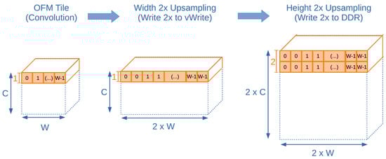
Figure 7.
Upsampling after convolution diagram.
The maxpool layers 10 and 12 are accelerated in isolation. Figure 8 presents a diagram for the input and output tiles used in each configured dataflow.
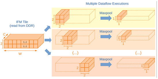
Figure 8.
Input and output tiles for the maxpool layer dataflows.
The first dataflow reads the complete layer input into the IFM tile memories. Each memory has a IFM tile. Each dataflow performs maxpooling over a input block and outputs a output block. Each output block is written to the main memory at the end of the dataflow configuration.
5. Results
This section presents the results of the proposed configurable object detector accelerator running the Tiny-YOLOv3 algorithm. Two different configurations of the architecture were implemented and tested in the SoC of the low-cost ZYNQ7020 FPGA. The configurations differ in the datapath size (8 and 16). The ZYNQ7020 SoC FPGA is a cost-optimized device targeting high-performance IoT devices. The accelerator was implemented in the programmable logic of the ZYNQ FPGA and integrated with the processing system that contains an ARM processor present in the ZYNQ architectures.
5.1. FPGA Resource Utilization
To illustrate the configurability of the accelerator, we implemented several designs with a different number of cores and determined the occupation of FPGA resources (see results in Table 5).
Table 5.
Resource utilization of the accelerator for 8-bit datawidth, four MACs per core, and different numbers of cores.
The configurations with more lines of cores were more expensive since each line adds an output buffer. For example, configurations and have the same number of cores, but the former needs more BRAMs and LUTs.
All configurations assume the same size for the on-chip memories to store IFMs and weights. If memory is available, these can be increased, which may improve the execution time. So, the occupation of BRAMs in Table 5 represents a minimum, assuming 32 KBytes of memory for each IFM buffer and 8 KBytes of memory for each weight memory.
The last two configurations ( and ) could be implemented, for example, in a smaller ZYNQ7010 SoC FPGA, which shows the scalability of the architecture to lower-density FPGAs.
The configuration with 13 lines of cores is usually preferred since the size of the feature maps considered by YOLO are multiples of 13. The other configurations can be used, but there will be a degradation in performance efficiency since in some iterations of the algorithm, some cores are not used. For example, running a feature map of size 26 in the architecture configured with eight lines of cores would need four iterations, and in the last iteration only two lines of cores would be running.
The accelerator was mapped into the ZYNQ7020 FPGA with quantizations of 8- and 16-bit. The 16-bit configuration was mainly considered for state-of-the-art comparison. Table 6 presents FPGA resource utilization of the accelerator for both configurations.
Table 6.
Resource utilization in a ZYNQ7020 FPGA.
In the low-cost ZYNQ7020 FPGA, the design is mainly constrained by the number of DSPs and BRAMs. The high utilization ratio of these hardware modules influences the operating frequency due to routing. Since a single DSP can implement two multiplications, the 8-bit solution doubles the number of MACs. It is possible to reduce the number of BRAMs of the 8-bit solution, but a higher number of BRAMs increases the number of layers that can benefit from the ping-pong technique of memories. Therefore, both solutions use the same number of memories.
5.2. Performance of the Accelerator
The Tiny-YOLOv3 was executed in the proposed accelerator with the configurations referenced in Table 5 but with full on-chip memory; that is, the on-chip memory to cache the input feature maps was maximized for all configurations (see the configuration parameters in Table 7).
Table 7.
Configuration parameters for the accelerator.
All architectures were synthesized with a clock frequency of 100 MHz and tested with Tiny-YOLOv3 (see the performance results in Table 8 and Figure 9).
Table 8.
Tiny-YOLOv3 execution times on the proposed architecture with different configurations of the core matrix.
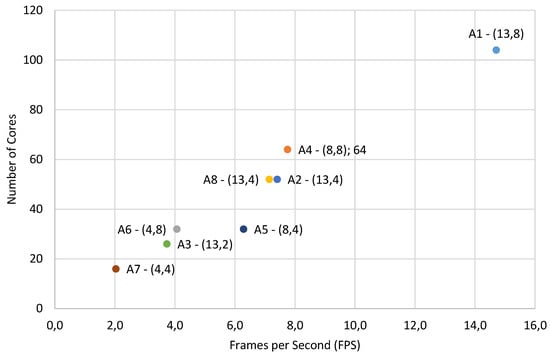
Figure 9.
The number of cores versus frames per second of each configuration of the architecture. The graphs indicate the configuration as number of lines of cores and number of columns of cores).
The most efficient solutions use 13 cores per column, since the size of feature maps are a multiple of 13. The A6 and A5 configurations use the same number of cores, but A6 is faster since the lower number of cores per column improves the efficiency. Both A8 and A2 architectures have the same number of cores, but architecture A8 is for 16-bit quantization. The 8-bit architecture is slightly faster and consumes fewer resources at the cost of 0.7 pp in accuracy.
Table 9 presents the Tiny-YOLOv3 network execution times on multiple platforms: Intel i7-8700 @ 3.2 GHz, GPU RTX 2080ti, and embedded GPU Jetson TX2 and Jetson Nano. The CPU and GPU results were obtained using the original Tiny-YOLOv3 network [42] with floating-point representation. The CPU result corresponds to the execution of Tiny-YOLOv3 implemented in C. The GPU result was obtained from the execution of Tiny-YOLOv3 in the Pytorch environment using CUDA libraries.
Table 9.
Tiny-YOLOv3 execution times on multiple platforms.
The Tiny-YOLOv3 on desktop CPUs is too slow. The inference time on an RTX 2080ti GPU showed a 109 speedup versus the desktop CPU. Using the proposed accelerator, the inference times were 140 and 68 ms, in the ZYNQ7020. The low-cost FPGA was 6X (16-bit) and 12X (8-bit) faster than the CPU with a small drop in accuracy of 1.4 and 2.1 points, respectively. Compared to the embedded GPU, the proposed architecture was 15% slower. The advantage of using the FPGA is the energy consumption. Jetson TX2 has a power close to 15 W, while the proposed accelerator has a power of around 0.5 W. The Nvidia Jetson Nano consumes a maximum of 10 W but is around slower than the proposed architecture.
5.3. Comparison with Other FPGA Implementations
The proposed implementation was compared with previous accelerators of Tiny-YOLOv3. We report the quantization, the operating frequency, the occupation of FPGA resources (DSP, LUTs, and BRAMs), and two performance metrics (execution time and frames per second). Additionally, we considered three metrics to quantify how efficiently the hardware resources were being used. Since different solutions usually have a different number of resources, it is fair to consider metrics to somehow normalize the results before comparison. FSP/kLUT, FPS/DSP, and FPS/BRAM determine the number of each resource that is used to produce a frame per second. The higher these values, the higher the utilization efficiency of these resources (see Table 10).
Table 10.
Performance comparison with other FPGA implementations.
The implementation in [39] is the only previous implementation with a Zynq 7020 SoC FPGA. This device has significantly fewer resources than the devices used in the other works. Our architecture implemented in the same device was 3.7X and 7.4X faster, depending on the quantization. For the same 16-bit quantization, the FPS/kLUT, FPS/DSP, and FPS/BRAM metrics of the proposed architecture were 3.5×, 2×, and 3× better, respectively. This shows that besides allowing smaller data quantizations, the architecture also improves the utilization efficiency of the FPGA resources for the same ZYNQ7020.
Compared to [40], the proposed work was slower and less efficient in terms of BRAMs but more efficient in terms of LUT and similarly efficient in terms DSP. The lower BRAM efficiency has to do with the fact that BRAM contents (weights and activations) are shared by multiple cores. An architecture with more cores has a higher FPS throughput, and each BRAM feeds more cores, which increases its utilization efficiency. However, this work used only a quarter of the resources, ran in a low-cost FPGA, and used the LUTs more efficiently. The work [38] used 8-bit quantization to increase the throughput at the cost of accuracy. Besides, it ran in a high-density FPGA not appropriate for IoT and only considered a limited target dataset. The number of resources was also not reported.
The work in [41] did not provide the performance of the architecture, only the occupied resources. The solution had a high utilization of LUTs and considered a quantization of 18 bits. This quantization takes advantage of the size of DSP multipliers () and BRAMs (can be configured with 72 of datawidth). However, it does not match the external memory bandwidth (usually 32 or 64 bits). This mismatch complicates data transfer.
6. Conclusions and Future Work
This study described the design of a configurable accelerator for object detection with YOLO in low-cost FPGA devices. The system achieved 7 and 14 FPS running the Tiny-YOLOv3 neural network with precision scores of 31.5 and 30.8 in the COCO 2017 test dataset (close to 32.9 of the original model with floating-point), for 16- and 8-bit quantizations, respectively. Given the drastic simplification achieved with the fixed-point representation, this accuracy loss is acceptable.
The configurability of the accelerator allows tailoring the design of the architecture for different FPGA sizes and Tiny-YOLO versions, as long as the CNN only uses the layers supported by the accelerator. The tested design was implemented with 16- and 8-bit fixed-point representation of weights, bias, and activations, but other quantization sizes can be considered.
The results are very promising, considering that a low-cost FPGA was utilized and that the solution is at least 6X faster than a state-of-the-art CPU. To improve the throughput of the object detection in IoT devices, two research directions can be followed. At the algorithmic level, model reduction with negligible accuracy loss is fundamental. Tiny models were a step towards this, and they keep improving. Otherwise, the high computing requirements of the backbone CNN of object detectors limit its applicability to edge devices. Quantization is another fundamental aspect since it also determines the computational requirements. In the case of the FPGA where the datapath of the computing units can be customized, this is a major optimization aspect. Finally, hardware-oriented algorithm optimizations benefit from a more efficient hardware design. An integrated algorithm–hardware development provides better solutions.
Author Contributions
Conceptualization, P.R.M., D.P., M.P.V. and J.T.d.S.; methodology, P.R.M., D.P., M.P.V., J.T.d.S. and H.C.N.; software, P.R.M. and D.P.; validation, P.R.M., D.P., M.P.V., J.T.d.S. and H.C.N.; formal analysis, P.R.M., D.P. and J.T.d.S.; investigation, P.R.M., D.P., M.P.V., J.T.d.S. and H.C.N.; resources, P.R.M., D.P., R.P.D., J.D.L. and J.T.d.S.; data curation, P.R.M., D.P., M.P.V., J.T.d.S., J.D.L. and R.P.D.; writing—original draft preparation, P.R.M. and D.P.; writing—review and editing, P.R.M. and M.P.V.; visualization, P.R.M., D.P., J.D.L. and R.P.D.; supervision, M.P.V., J.T.d.S. and H.C.N.; project administration, J.T.d.S.; funding acquisition, J.T.d.S. All authors have read and agreed to the published version of the manuscript.
Funding
This work was supported in part by the Fundação para a Ciência e Tecnologia (FCT) under Grant UIDB/50021/2020 and in part by the projects PTDC/EEI-HAC/30848/2017, through INESC-ID and IPL/IDI&CA/2020/TRAINEE/ISEL through Instituto Politécnico de Lisboa.
Data Availability Statement
Not applicable, the study does not report any data.
Conflicts of Interest
The authors declare no conflict of interest.
References
- Jiao, L.; Zhang, F.; Liu, F.; Yang, S.; Li, L.; Feng, Z.; Qu, R. A Survey of Deep Learning-Based Object Detection. IEEE Access 2019, 7, 128837–128868. [Google Scholar] [CrossRef]
- Liu, L.; Ouyang, W.; Wang, X.; Fieguth, P.W.; Chen, J.; Liu, X.; Pietikäinen, M. Deep Learning for Generic Object Detection: A Survey. Int. J. Comput. Vis. 2020, 128, 261–368. [Google Scholar] [CrossRef] [Green Version]
- Unlu, E.; Zenou, E.; Riviere, N.; Dupouy, P.E. Deep learning-based strategies for the detection and tracking of drones using several cameras. IPSJ Trans. Comput. Vis. Appl. 2019, 11, 7. [Google Scholar] [CrossRef] [Green Version]
- Simhambhatla, R.; Okiah, K.; Kuchkula, S.; Slater, R. Self-Driving Cars: Evaluation of Deep Learning Techniques for Object Detection in Different Driving Conditions. SMU Data Sci. Rev. 2019, 2, 23. [Google Scholar]
- Merenda, M.; Porcaro, C.; Iero, D. Edge Machine Learning for AI-Enabled IoT Devices: A Review. Sensors 2020, 20, 2533. [Google Scholar] [CrossRef]
- Mahony, N.O.; Campbell, S.; Carvalho, A.; Harapanahalli, S.; Velasco-Hernández, G.A.; Krpalkova, L.; Riordan, D.; Walsh, J. Deep Learning vs. Traditional Computer Vision. CoRR. arXiv 2019, arXiv:1910.13796. [Google Scholar]
- Zhao, Z.; Zheng, P.; Xu, S.; Wu, X. Object Detection With Deep Learning: A Review. IEEE Trans. Neural Networks Learn. Syst. 2019, 30, 3212–3232. [Google Scholar] [CrossRef] [Green Version]
- Girshick, R.; Donahue, J.; Darrell, T.; Malik, J. Rich Feature Hierarchies for Accurate Object Detection and Semantic Segmentation. In Proceedings of the 2014 IEEE Conference on Computer Vision and Pattern Recognition, Columbus, OH, USA, 24–28 June 2014; pp. 580–587. [Google Scholar] [CrossRef] [Green Version]
- Girshick, R. Fast R-CNN. In Proceedings of the 2015 IEEE International Conference on Computer Vision (ICCV), Santiago, Chile, 7–13 December 2015; pp. 1440–1448. [Google Scholar] [CrossRef]
- Dai, J.; Li, Y.; He, K.; Sun, J. R-FCN: Object Detection via Region-Based Fully Convolutional Networks. In Proceedings of the 30th International Conference on Neural Information Processing Systems (NIPS’16), Long Beach, CA, USA, 4–9 December 2017; Curran Associates Inc.: Red Hook, NY, USA, 2016; pp. 379–387. [Google Scholar]
- Ren, S.; He, K.; Girshick, R.; Sun, J. Faster R-CNN: Towards Real-Time Object Detection with Region Proposal Networks. IEEE Trans. Pattern Anal. Mach. Intell. 2017, 39, 1137–1149. [Google Scholar] [CrossRef] [Green Version]
- He, K.; Gkioxari, G.; Dollár, P.; Girshick, R. Mask R-CNN. In Proceedings of the 2017 IEEE International Conference on Computer Vision (ICCV), Venice, Italy, 22–29 October 2017; pp. 2980–2988. [Google Scholar] [CrossRef]
- Redmon, J.; Divvala, S.; Girshick, R.; Farhadi, A. You Only Look Once: Unified, Real-Time Object Detection. In Proceedings of the 2016 IEEE Conference on Computer Vision and Pattern Recognition (CVPR), Las Vegas, NV, USA, 27–30 June 2016; pp. 779–788. [Google Scholar] [CrossRef] [Green Version]
- Redmon, J.; Farhadi, A. YOLO9000: Better, Faster, Stronger. In Proceedings of the 2017 IEEE Conference on Computer Vision and Pattern Recognition (CVPR), Honolulu, HI, USA, 21–26 July 2017; pp. 6517–6525. [Google Scholar] [CrossRef] [Green Version]
- Redmon, J.; Farhadi, A. YOLOv3: An Incremental Improvement. arXiv 2018, arXiv:1804.02767. [Google Scholar]
- Bochkovskiy, A.; Wang, C.Y.; Liao, H.Y.M. YOLOv4: Optimal Speed and Accuracy of Object Detection. arXiv 2020, arXiv:cs.CV/2004.10934. [Google Scholar]
- Lin, T.; Goyal, P.; Girshick, R.; He, K.; Dollár, P. Focal Loss for Dense Object Detection. IEEE Trans. Pattern Anal. Mach. Intell. 2020, 42, 318–327. [Google Scholar] [CrossRef] [Green Version]
- Carranza-García, M.; Torres-Mateo, J.; Lara-Benítez, P.; García-Gutiérrez, J. On the Performance of One-Stage and Two-Stage Object Detectors in Autonomous Vehicles Using Camera 621 Data. Remote Sens. 2021, 13, 89. [Google Scholar] [CrossRef]
- Véstias, M.P.; Duarte, R.P.; de Sousa, J.T.; Neto, H.C. Moving Deep Learning to the Edge. Algorithms 2020, 13, 125. [Google Scholar] [CrossRef]
- Sze, V.; Chen, Y.; Yang, T.; Emer, J.S. Efficient Processing of Deep Neural Networks: A Tutorial and Survey. Proc. IEEE 2017, 105, 2295–2329. [Google Scholar] [CrossRef] [Green Version]
- Feng, X.; Jiang, Y.; Yang, X.; Du, M.; Li, X. Computer vision algorithms and hardware implementations: A survey. Integration 2019, 69, 309–320. [Google Scholar] [CrossRef]
- Redmon, J.; Divvala, S.; Girshick, R.; Farhadi, A. You Only Look Once: Unified, Real-Time Object Detection. arXiv 2015, arXiv:1506.02640. [Google Scholar]
- Gonçalves, A.; Peres, T.; Véstias, M. Exploring Data Size to Run Convolutional Neural Networks in Low Density FPGAs. In Applied Reconfigurable Computing; Hochberger, C., Nelson, B., Koch, A., Woods, R., Diniz, P., Eds.; Springer International Publishing: Cham, Switzerland, 2019; pp. 387–401. [Google Scholar]
- Ma, Y.; Suda, N.; Cao, Y.; Seo, J.; Vrudhula, S. Scalable and modularized RTL compilation 637 of Convolutional Neural Networks onto FPGA. In Proceedings of the 26th International Conference on Field Programmable Logic and Applications (FPL), Lausanne, Switzerland, 29 August–2 September 2016; pp. 1–8. [Google Scholar] [CrossRef]
- Krizhevsky, A.; Sutskever, I.; Hinton, G.E. ImageNet Classification with Deep Convolutional Neural Networks. In Proceedings of the 25th International Conference on Neural Information Processing Systems—Volume 1 (NIPS’12); Curran Associates Inc.: Red Hook, NY, USA, 2012; pp. 1097–1105. [Google Scholar]
- Lin, M.; Chen, Q.; Yan, S. Network In Network. arXiv 2013, arXiv:cs.NE/1312.4400. [Google Scholar]
- Kluska, P.; Zieba, M. Post-training Quantization Methods for Deep Learning Models. In Intelligent Information and Database Systems; Nguyen, N.T., Jearanaitanakij, K., Selamat, A., Trawiński, B., Chittayasothorn, S., Eds.; Springer International Publishing: Cham, Switzerland, 2020; pp. 467–479. [Google Scholar]
- Véstias, M.P. A Survey of Convolutional Neural Networks on Edge with Reconfigurable Computing. Algorithms 2019, 12, 154. [Google Scholar] [CrossRef] [Green Version]
- Qiu, J.; Wang, J.; Yao, S.; Guo, K.; Li, B.; Zhou, E.; Yu, J.; Tang, T.; Xu, N.; Song, S.; et al. Going Deeper with Embedded FPGA Platform for Convolutional Neural Network. In Proceedings of the 2016 ACM/SIGDA International Symposium on Field-Programmable Gate Arrays, Monterey, CA, USA, 21–23 February 2016; pp. 26–35. [Google Scholar] [CrossRef]
- Zhang, C.; Li, P.; Sun, G.; Guan, Y.; Xiao, B.; Cong, J. Optimizing FPGA-Based Accelerator Design for Deep Convolutional Neural Networks. In Proceedings of the 2015 ACM/SIGDA International Symposium on Field-Programmable Gate Arrays, Monterey, CA, USA, 22–24 February 2015; pp. 161–170. [Google Scholar] [CrossRef]
- Suda, N.; Chandra, V.; Dasika, G.; Mohanty, A.; Ma, Y.; Vrudhula, S.; Seo, J.s.; Cao, Y. Throughput-Optimized OpenCL-Based FPGA Accelerator for Large-Scale Convolutional Neural Networks. In Proceedings of the 2016 ACM/SIGDA International Symposium on Field-Programmable Gate Arrays, Monterey, CA, USA, 21–23 February 2016; pp. 16–25. [Google Scholar] [CrossRef]
- Ma, Y.; Cao, Y.; Vrudhula, S.; Seo, J.S. Optimizing Loop Operation and Dataflow in FPGA Acceleration of Deep Convolutional Neural Networks. In Proceedings of the 2017 ACM/SIGDA International Symposium on Field-Programmable Gate Arrays (FPGA ’17), Monterey, CA, USA, 22–24 February 2017; ACM: New York, NY, USA, 2017; pp. 45–54. [Google Scholar] [CrossRef]
- Véstias, M.P.; Duarte, R.P.; de Sousa, J.T.; Neto, H.C. A fast and scalable architecture to run convolutional neural networks in low density FPGAs. Microprocess. Microsyst. 2020, 77, 103136. [Google Scholar] [CrossRef]
- Abdelouahab, K.; Pelcat, M.; Sérot, J.; Berry, F. Accelerating CNN inference on FPGAs: A Survey. CoRR. arXiv 2018, arXiv:1806.01683. [Google Scholar]
- Wei, G.; Hou, Y.; Cui, Q.; Deng, G.; Tao, X.; Yao, Y. YOLO Acceleration using FPGA Architecture. In Proceedings of the 2018 IEEE/CIC International Conference on Communications in China (ICCC), Beijing, China, 16–18 August 2018; pp. 734–735. [Google Scholar] [CrossRef]
- Xu, X.; Liu, B. FCLNN: A Flexible Framework for Fast CNN Prototyping on FPGA with OpenCL and Caffe. In Proceedings of the 2018 International Conference on Field-Programmable Technology (FPT), Okinawa, Japan, 10–14 December 2018; pp. 238–241. [Google Scholar] [CrossRef]
- Nakahara, H.; Yonekawa, H.; Fujii, T.; Sato, S. A Lightweight YOLOv2: A Binarized CNN with A Parallel Support Vector Regression for an FPGA. In Proceedings of the 2018 ACM/SIGDA International Symposium on Field-Programmable Gate Arrays (FPGA ’18), Monterey, CA, USA, 25–27 February 2018; Association for Computing Machinery: New York, NY, USA, 2018; pp. 31–40. [Google Scholar] [CrossRef]
- Oh, S.; You, J.H.; Kim, Y.K. Implementation of Compressed YOLOv3-tiny on FPGA-SoC. In Proceedings of the 2020 IEEE International Conference on Consumer Electronics—Asia (ICCE-Asia), Gangneung, Korea, 1–3 November 2020; pp. 1–4. [Google Scholar] [CrossRef]
- Yu, Z.; Bouganis, C.S. A Parameterisable FPGA-Tailored Architecture for YOLOv3-Tiny. In Applied Reconfigurable Computing. Architectures, Tools, and Applications; Rincón, F., Barba, J., So, H.K.H., Diniz, P., Caba, J., Eds.; Springer International Publishing: Cham, Switzerland, 2020; pp. 330–344. [Google Scholar]
- Pestana, D.; Miranda, P.R.; Lopes, J.D.; Duarte, R.P.; Véstias, M.P.; Neto, H.C.; De Sousa, J.T. A Full Featured Configurable Accelerator for Object Detection with YOLO. IEEE Access 2021, 9, 75864–75877. [Google Scholar] [CrossRef]
- Ahmad, A.; Pasha, M.A.; Raza, G.J. Accelerating Tiny-YOLOv3 using FPGA-Based Hardware/Software Co-Design. In Proceedings of the 2020 IEEE International Symposium on Circuits and Systems (ISCAS), Sevilla, Spain, 10–21 October 2020; pp. 1–5. [Google Scholar] [CrossRef]
- Redmond, J. Darknet. Available online: https://github.com/pjreddie/darknet (accessed on 29 October 2021).
- Ayoub, N.; Schneider-Kamp, P. Real-Time On-Board Deep Learning Fault Detection for Autonomous UAV Inspections. Electronics 2021, 10, 1091. [Google Scholar] [CrossRef]
Publisher’s Note: MDPI stays neutral with regard to jurisdictional claims in published maps and institutional affiliations. |
© 2021 by the authors. Licensee MDPI, Basel, Switzerland. This article is an open access article distributed under the terms and conditions of the Creative Commons Attribution (CC BY) license (https://creativecommons.org/licenses/by/4.0/).