Adaptive Coherent Receiver Settings for Optimum Channel Spacing in Gridless Optical Networks


Abstract
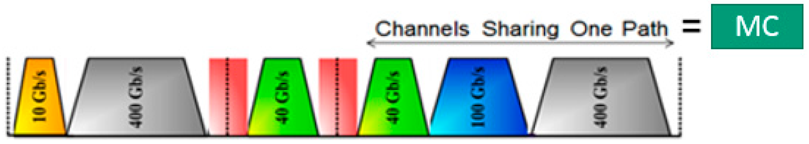
:1. Introduction
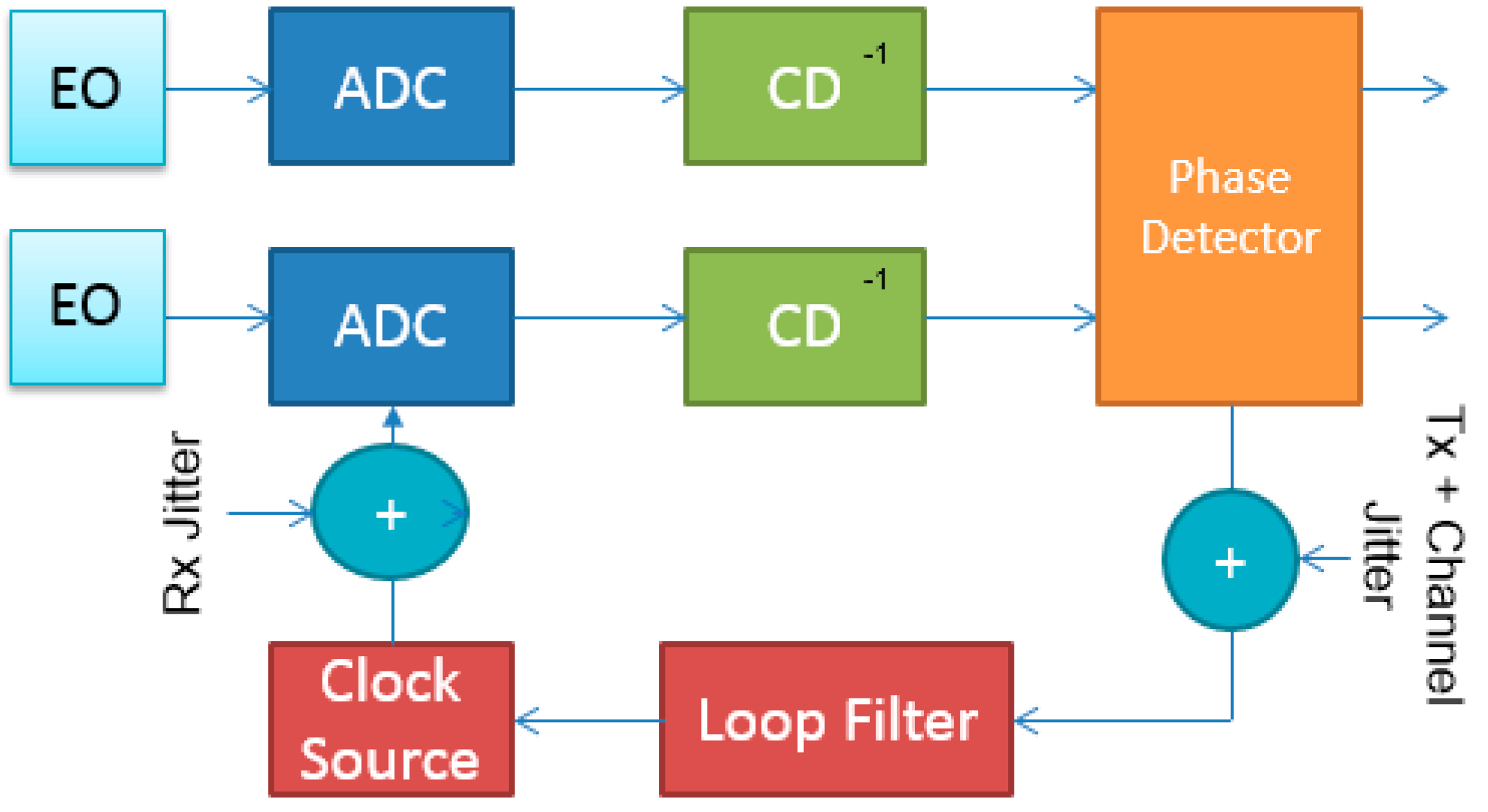
2. Clock Recovery in Coherent Optical Receivers
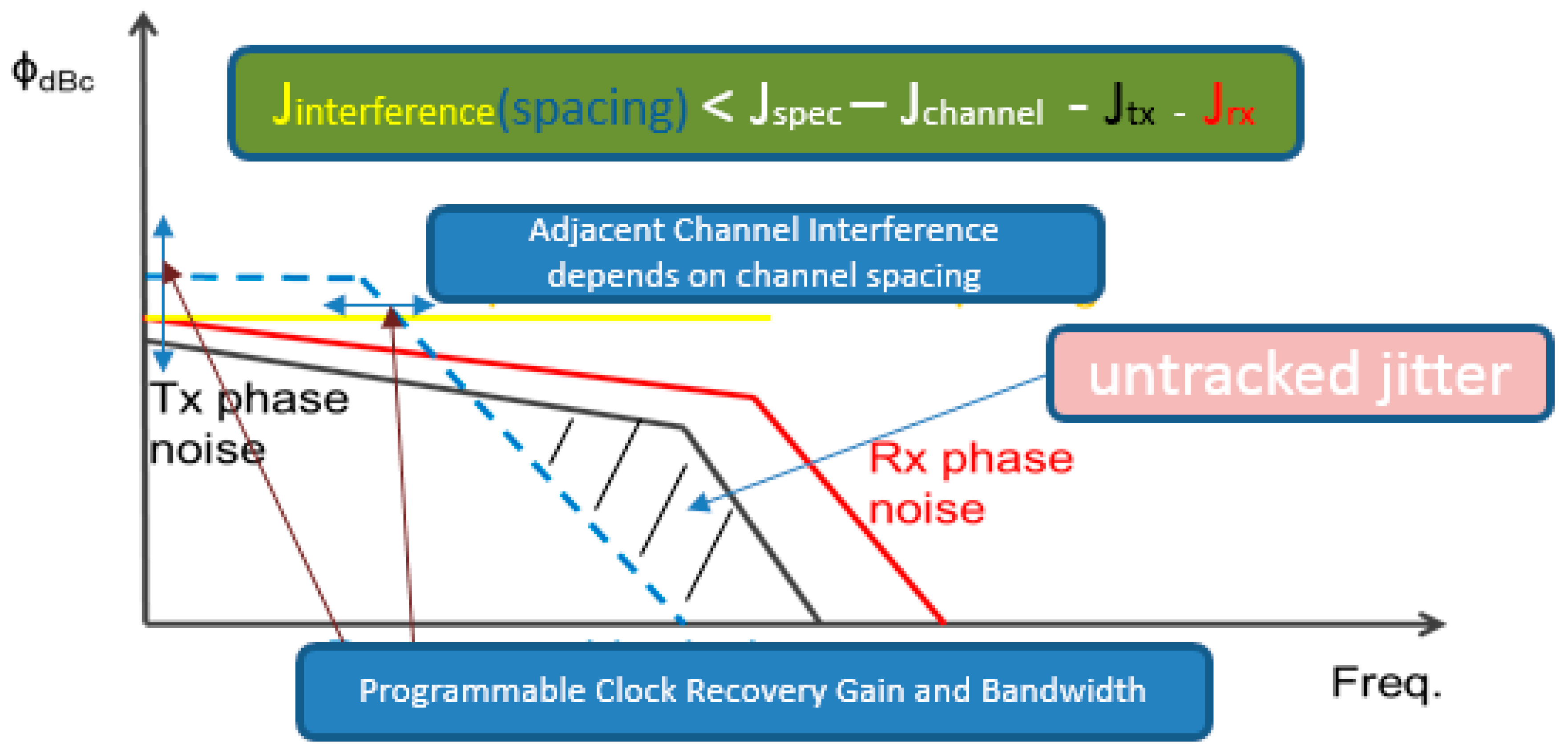
2.1. Sources of Jitter
- Amplified spontaneous emission (ASE) induced by optical line amplifiers can shift the pulse from its ideal location [17].
- CD, which its bulk part should be compensated before being able to digitally recover timing information, although a certain residual dispersion tolerance is anticipated but it comes with a penalty. In [20], when CD is convoluted with the phase noise of the local oscillator it causes timing jitter.
- Q: Resonator loaded QP: Resonator power
- : Flicker noise corner
- : Offset from carrier
- : RF frequency
- F: Oscillator noise figure
- K: Boltzmann’s constant
- Temp: Temperature
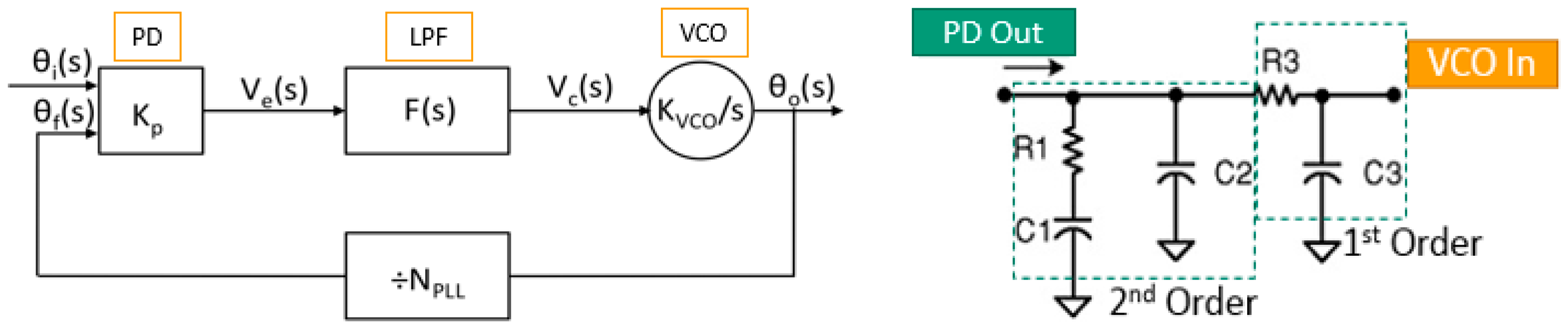
2.2. PLL Basics
3. Proposed Clock Recovery Circuit and Method
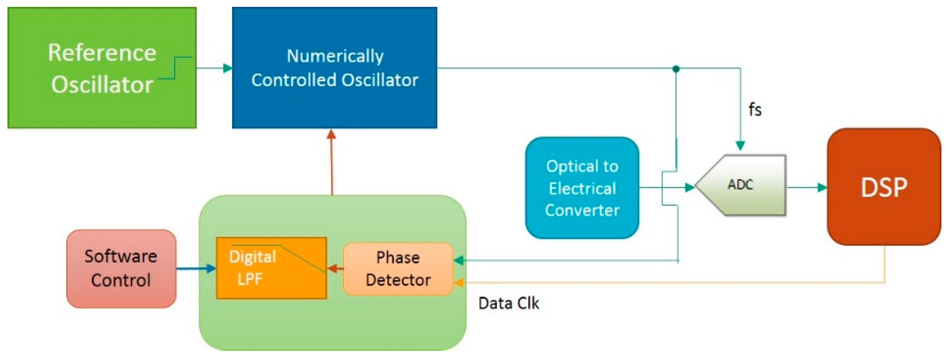
3.1. Circuit
3.2. Phase Detector
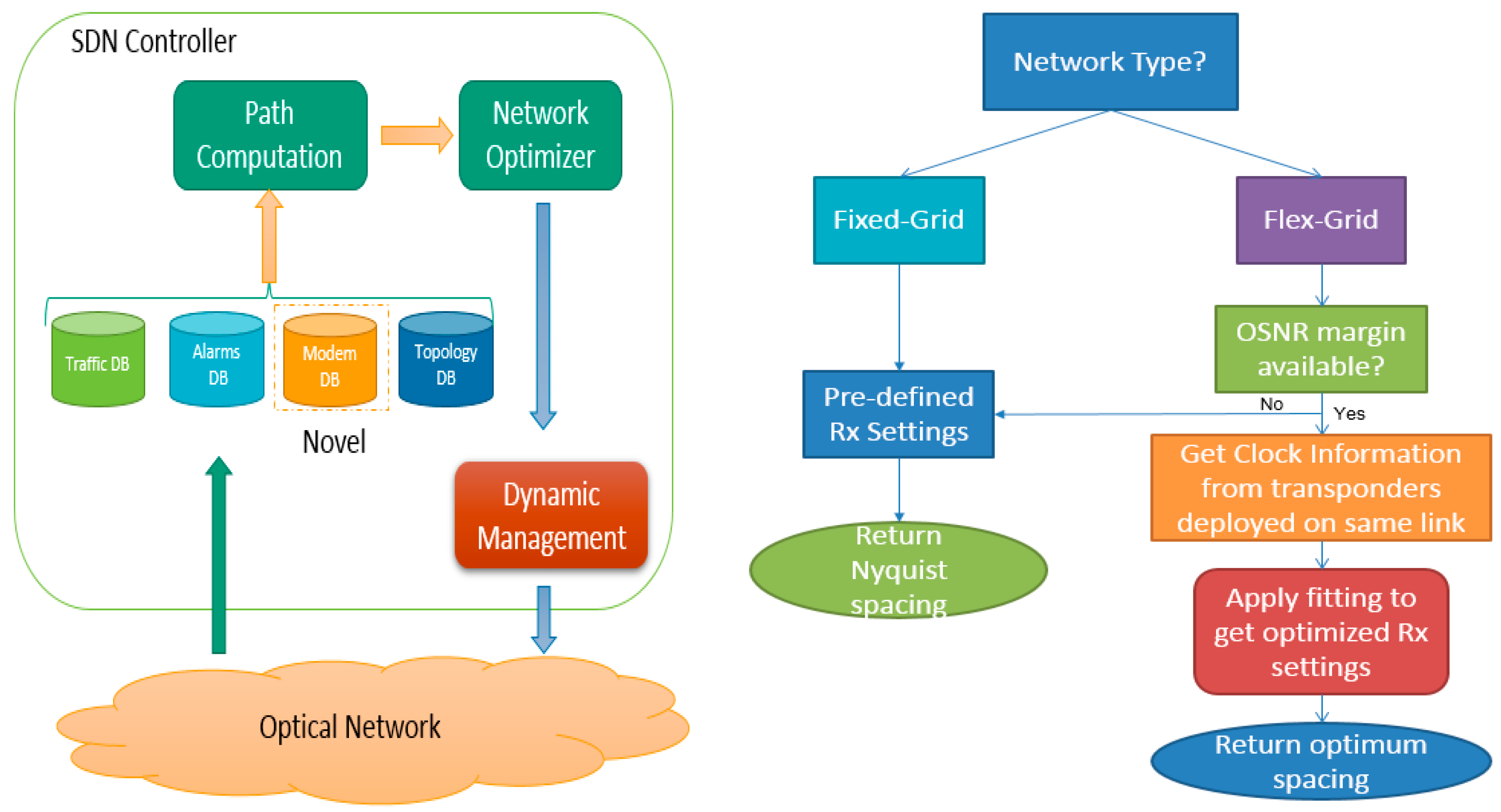
3.3. Method Integrated in SDN Framework
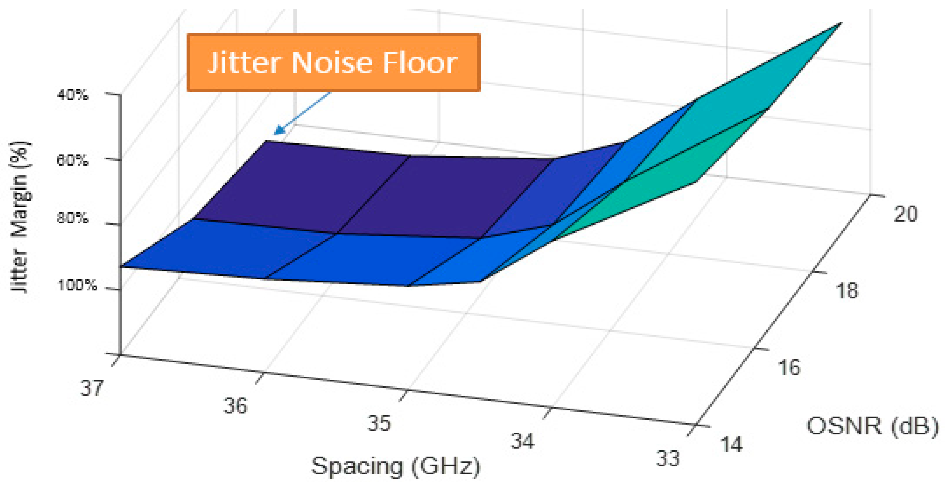
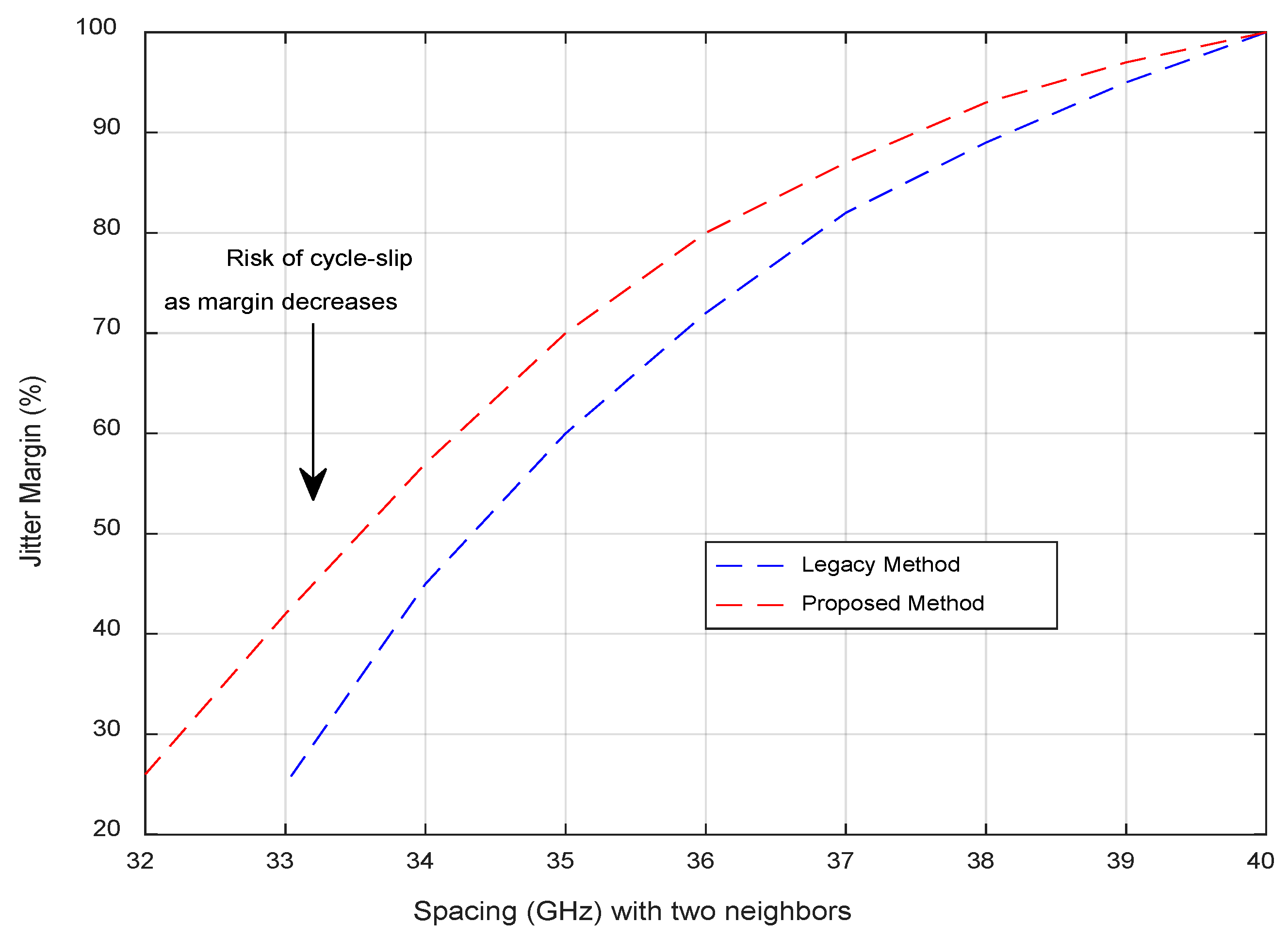
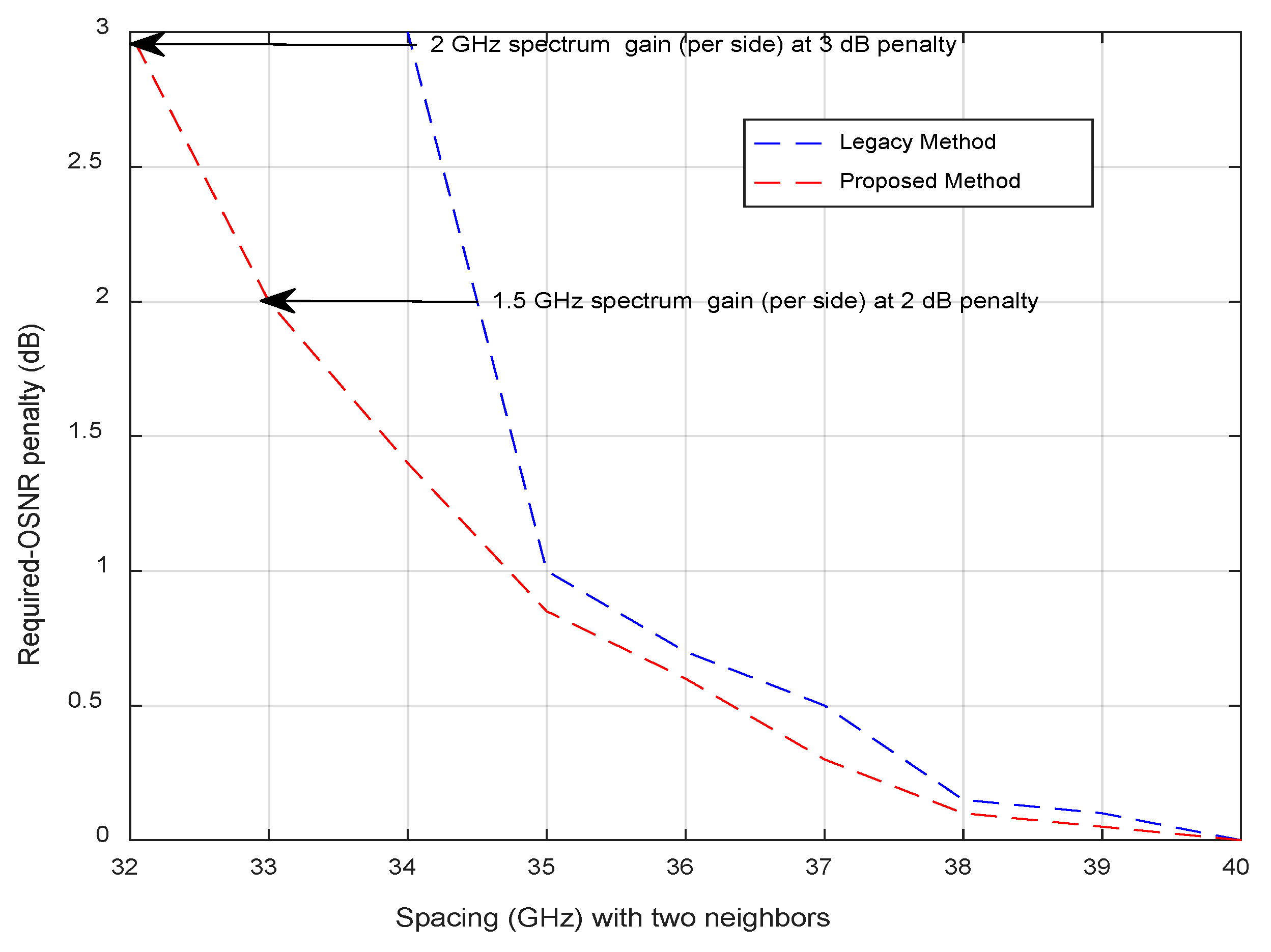
4. Experimental Results and Discussions
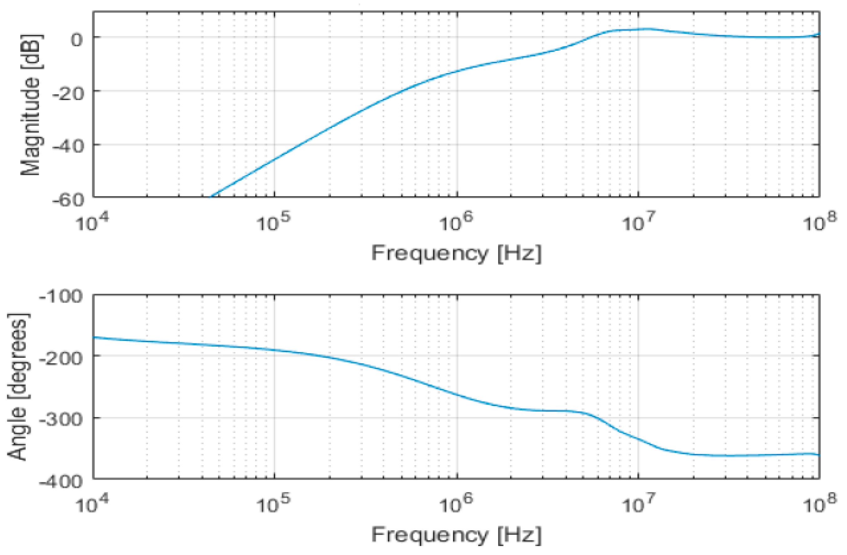
4.1. Experimental Setup
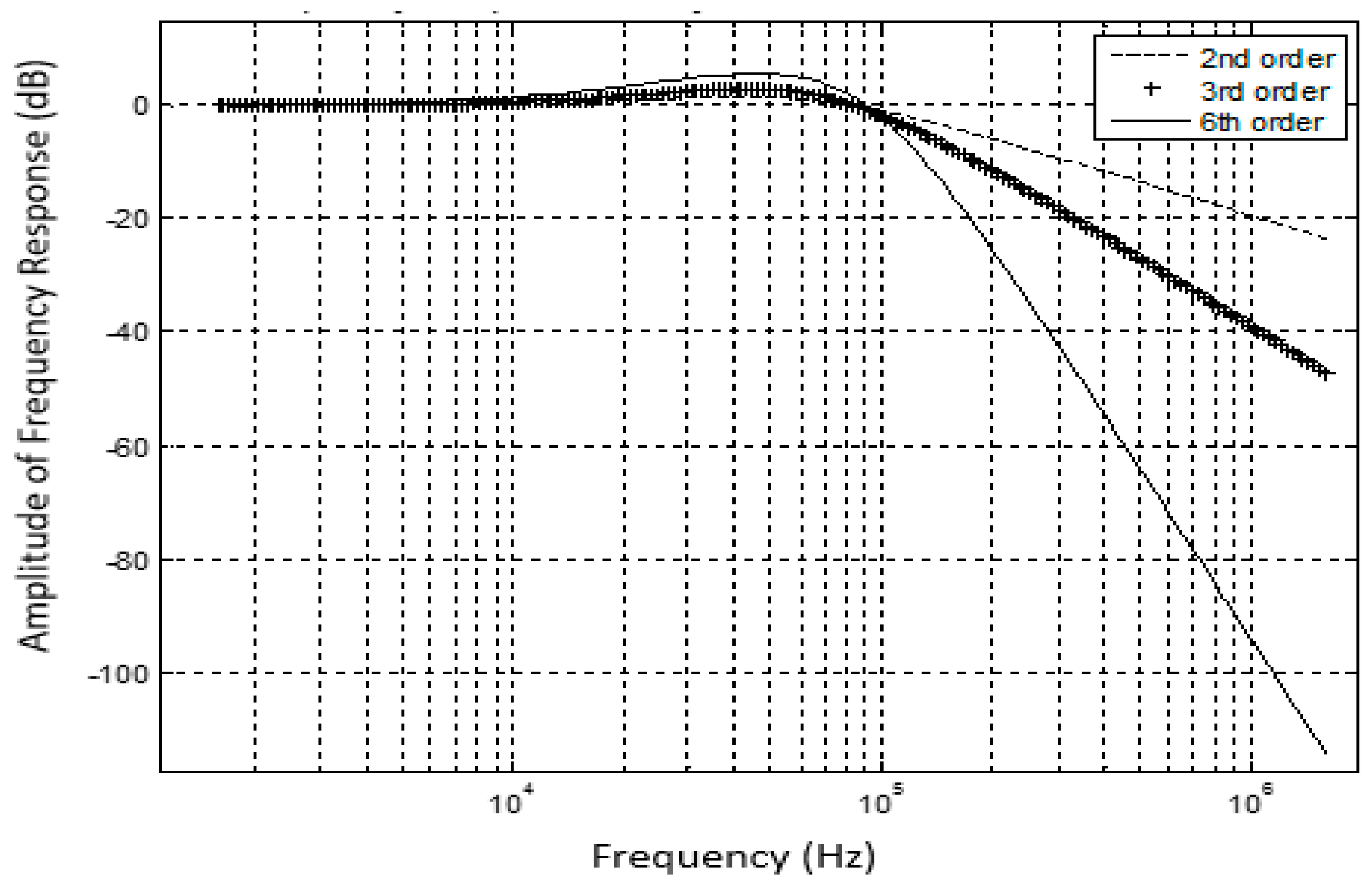
4.2. Results and Discussion
5. Conclusions
6. Patents
Author Contributions
Funding
Conflicts of Interest
References
- Frisken, S.; Baxter, G.; Abakoumov, D.; Zhou, H.; Clarke, I.; Poole, S. Flexible and Grid-less Wavelength Selective Switch using LCOS Technology. In Proceedings of the 2011 Optical Fiber Communication Conference and Exposition and the National Fiber Optic Engineers Conference, Los Angeles, CA, USA, 6–10 March 2011. [Google Scholar] [CrossRef]
- Okoshi, T.; Kikuchi, K. Coherent Optical Communication Systems; KTK Scientific Publisher: Tokyo, Japan, 1988; Chapter 1. [Google Scholar]
- ITU. G.694.1: Spectral Grids for WDM Applications: DWDM Frequency Grid; ITU, 2012. Available online: https://www.itu.int/rec/T-REC-G.694.1-201202-I/en (accessed on 24 September 2019).
- Ben-Hamida, N.; Sitch, J.; Flemke, P.; Pollex, D.; Schvan, P.; Greshishchev, Y.; Wang, S.C.; Falt, C. Clock recovery for a 40 Gb/s QPSK optical receiver. In Proceedings of the 2009 16th IEEE International Conference on Electronics, Circuits and Systems (ICECS 2009), Yasmine Hammamet, Tunisia, 13–16 December 2009; pp. 695–698. [Google Scholar]
- Schuh, K.; Buchali, F.; Idler, W.; Hu, Q.; Templ, W.; Bielik, A.; Altenhain, L.; Langenhagen, H.; Rupeter, J.; Duemler, U.; et al. 100 GSa/s BiCMOS DAC Supporting 400 Gb/s Dual Channel Transmission. In Proceedings of the 42nd European Conference on Optical Communication (ECOC 2016), Dusseldorf, Germany, 18–22 September 2016; pp. 1–3. [Google Scholar]
- Zibar, D.; Bianciotto, A.; Wang, Z.; Napoli, A.; Spinnler, B. Analysis and dimensioning of fully digital clock recovery for 112 gb/s coherent polmux QPSK systems. In Proceedings of the 2009 35th European Conference on Optical Communication, Vienna, Austria, 20–24 September 2009; pp. 1–2. [Google Scholar]
- Hauske, F.N.; Stojanovic, N.; Xie, C.; Chen, M. Impact of optical channel distortions to digital timing recovery in digital coherent transmission systems. In Proceedings of the 2010 12th International Conference on Transparent Optical Networks, Munich, Germany, 27 June–1 July 2010; pp. 1–4. [Google Scholar]
- Stojanović, N.; Xie, C.; Zhao, Y.; Mao, B.; Gonzalez, N.G. A circuit enabling clock extraction in coherent receivers. In Proceedings of the 2012 38th European Conference and Exhibition on Optical Communications, Amsterdam, Netherlands, 16–20 September 2012; pp. 1–3. [Google Scholar]
- Diniz, J.C.M.; Piels, M.; Zibar, D. Performance Evaluation of Clock Recovery for Coherent Mode Division Multiplexed Systems. In Proceedings of the Optical Fiber Communication Conference, Los Angeles, CA, USA, 19–23 March 2017. [Google Scholar]
- Diniz, J.; Da Ros, F.; Zibar, D. Clock Recovery Challenges in DSP-Based Coherent Single-Mode and Multi-Mode Optical Systems. Future Internet 2018, 10, 59. [Google Scholar] [CrossRef]
- Stojanović, N.; Chuan, X. Clock recovery in coherent optical receivers. In Proceedings of the 2015 Optical Fiber Communications Conference and Exhibition (OFC), Los Angeles, CA, USA, 22–26 March 2015; pp. 1–3. [Google Scholar]
- Yan, M.; Tao, Z.; Dou, L.; Li, L.; Zhao, Y.; Hoshida, T.; Rasmussen, J.C. Digital clock recovery algorithm for Nyquist signal. In Proceedings of the 2013 Optical Fiber Communication Conference and Exposition and the National Fiber Optic Engineers Conference (OFC/NFOEC), Anaheim, CA, USA, 17–21 March 2013; pp. 1–3. [Google Scholar]
- Eramo, V.; Lavacca, F.G. Proposal and Investigation of a Reconfiguration Cost Aware Policy for Resource Allocation in Multi-Provider NFV Infrastructures Interconnected by Elastic Optical Networks. IEEE J. Light. Technol. 2019, 37, 4098–4114. [Google Scholar] [CrossRef]
- Eramo, V.; Lavacca, F.G. Optimizing the cloud resources, bandwidth and deployment costs in multi-providers network function virtualization environment. IEEE Access 2019, 7, 46898–46916. [Google Scholar] [CrossRef]
- Caria, M.; Jukan, A.; Hoffmann, M. A Performance Study of Network Migration to SDN-enabled Traffic Engineering. In Proceedings of the 2013 IEEE Global Communications Conference (Globecom 2013), Atlanta, GA, USA, 9–13 December 2013. [Google Scholar]
- Stojanović, N.; Zhao, Y.; Xie, C. Feed-forward and feedback timing recovery for Nyquist and faster than Nyquist systems. In Proceedings of the Optical Fiber Communication Conference 2014 (OFC 2014), San Francisco, CA, USA, 9–13 March 2014. [Google Scholar]
- Grigoryan, V.; Menyuk, C.; Mu, R.-M. Calculation of timing and amplitude jitter in dispersion-managed optical fiber communications using linearization. J. Light. Technol. 1999, 17, 1347–1356. [Google Scholar] [CrossRef]
- Eiselt, M.; Shtaif, M.; Garrett, L.D. Contribution of timing jitter and amplitude distortion to XPM system penalty in WDM systems. IEEE Photonics Technol. Lett. 1999, 11, 748–750. [Google Scholar] [CrossRef]
- Eiselt, M. The impact of non-linear fiber effects on fiber choice for ultimate transmission capacity. In Proceedings of the Optical Fiber Communication Conference 2000, Baltimore, MD, USA, 7 March 2000; Volume 1, pp. 58–60. [Google Scholar]
- Oda, S.; Ohshima, C.; Tanaka, T.; Tanimura, T.; Nakashima, H.; Koizumi, N.; Hoshida, T.; Zhang, H.; Tao, Z.; Rasmussen, J.C. Interplay between local oscillator phase noise and electrical chromatic dispersion compensation in digital coherent transmission system. In Proceedings of the 36th European Conference and Exhibition on Optical Communication, Torino, Italy, 19–23 September 2010; pp. 1–3. [Google Scholar]
- Leeson, D.B. A Simple Model of Feedback Oscillator Noise Spectrum. Proc. IEEE 1996, 54, 329–330. [Google Scholar] [CrossRef]
- Mehrotra, A. Noise analysis of phase-locked loops. IEEE Trans. Circuits Syst. I 2002, 49, 1309–1316. [Google Scholar] [CrossRef]
- Almeida, T.M.; Piedade, M.S. High performance analog and digital PLL design. In Proceedings of the 1999 IEEE International Symposium on Circuits and Systems VLSI (Cat. No.99CH36349), Orlando, FL, USA, 30 May–2 June 1999; Volume 4, pp. 394–397. [Google Scholar]
- Hsieh, G.C.; Hung, J.C. Phase-locked loop techniques—A survey. IEEE Trans. Ind. Electron. 1996, 43, 609–615. [Google Scholar] [CrossRef]
- Brownlee, M.; Hanumolu, P.K.; Mayaram, K.; Moon, U. A 0.5-GHz to 2.5-GHz PLL With Fully Differential Supply Regulated Tuning. IEEE J. Solid State Circuits 2006, 41, 2720–2728. [Google Scholar] [CrossRef]
- Gardner, F.M. A BPSK/QPSK timing-error detector for sampled receivers. IEEE Trans. Commun. 1986, 34, 423–429. [Google Scholar] [CrossRef]
- Wang, D.; Lu, K.; Rasmussen, P.O.; Yang, Z. Comparative study of low-pass filter and phase-locked loop type speed filters for sensorless control of AC drives. CES Trans. Electr. Mach. Syst. 2017, 1, 207–215. [Google Scholar]
- OIF 400ZR. Available online: https://www.oiforum.com/technical-work/hot-topics/400zr-2/ (accessed on 4 August 2019).
- Mehta, P.; Gaudette, J.; Li, J. Flexible grid spacing using Nyquist-shaped channels for undersea transmission. In Proceedings of the Photonics North 2014, International Society for Optics and Photonics, Montréal, QC, Canada, 28–30 May 2014. [Google Scholar]
- Huang, L.; Wang, D.; Lau, A.P.T.; Lu, C.; He, S. Performance analysis of blind timing phase estimators for digital coherent receivers. Opt. Express 2014, 22, 6749–6763. [Google Scholar] [CrossRef] [PubMed]

© 2019 by the authors. Licensee MDPI, Basel, Switzerland. This article is an open access article distributed under the terms and conditions of the Creative Commons Attribution (CC BY) license (http://creativecommons.org/licenses/by/4.0/).
Share and Cite
Abdo, A.; Aouini, S.; Riaz, B.; Ben-Hamida, N.; D’Amours, C. Adaptive Coherent Receiver Settings for Optimum Channel Spacing in Gridless Optical Networks. Future Internet 2019, 11, 206. https://doi.org/10.3390/fi11100206
Abdo A, Aouini S, Riaz B, Ben-Hamida N, D’Amours C. Adaptive Coherent Receiver Settings for Optimum Channel Spacing in Gridless Optical Networks. Future Internet. 2019; 11(10):206. https://doi.org/10.3390/fi11100206
Chicago/Turabian StyleAbdo, Ahmad, Sadok Aouini, Bilal Riaz, Naim Ben-Hamida, and Claude D’Amours. 2019. "Adaptive Coherent Receiver Settings for Optimum Channel Spacing in Gridless Optical Networks" Future Internet 11, no. 10: 206. https://doi.org/10.3390/fi11100206
APA StyleAbdo, A., Aouini, S., Riaz, B., Ben-Hamida, N., & D’Amours, C. (2019). Adaptive Coherent Receiver Settings for Optimum Channel Spacing in Gridless Optical Networks. Future Internet, 11(10), 206. https://doi.org/10.3390/fi11100206