Article

Adaptive Coherent Receiver Settings for Optimum Channel Spacing in Gridless Optical Networks

1
School of Electrical Engineering and Computer Science, University of Ottawa, Ottawa, ON K1N 6N5, Canada
2
Ciena Corporation, Ottawa, ON K2K 0L1, Canada
*
Author to whom correspondence should be addressed.
Future Internet 2019, 11(10), 206; https://doi.org/10.3390/fi11100206
Submission received: 5 August 2019 / Revised: 19 September 2019 / Accepted: 23 September 2019 / Published: 25 September 2019

Abstract

:
In this paper, we propose a novel circuit and system to optimize the spacing between optical channels in gridless (also called flexible-grid or elastic) networking. The method will exploit the beginning-of-life link margin by enabling the channel to operate in super-Nyquist dense wavelength division multiplexing mode. We present the work in the context of software-defined networking and high-speed optical flexible-rate transponders. The clock recovery scheme allows the mitigation of jitter by decoupling the contribution of high-jitter noise sources from the clock recovery loop. The method and associated algorithm are experimentally verified where a spectrum gain of up to 2 GHz in spacing between two channels in the Media Channel (MC) is obtained compared to conventional clocking strategies. We showed that the improvement is equivalent to increasing throughput, in a data-center interconnect scenario, by up to 300 giga-bits per second per route.

1. Introduction

The cloud computing era is pushing operators to upgrade to more autonomous and agile management of traffic demands. With optical fibers providing the backbone of modern networks, dense wavelength division multiplexing (DWDM) links should therefore be more flexible. Optical networks evolved from point-to-point links, to fixed add/drop where multiplexing ports are specified per wavelength, to fixed 50GHz bandwidth reconfigurable optical add-drop multiplexers (ROADMs) with internal variable optical attenuators (VOAs) and now with the current high-end generation of Wavelength Selective Switches (WSSs), such as the one based on Liquid Crystal on Silicon (LCOS) technology [1]. The latter will enable elastic spectral resolution in multiples of 12.5 GHz. Such flexibility in the photonics transport layer is completed with advancement in software-defined coherent transponders. The latter are typically dual-polarization coherent optical receivers coupled with high-speed data converters with intelligent digital signal processing [2]. With centralized control and high-level applications, software-defined networking (SDN) is emerging as the preferred network architecture approach. The paradigm is based on monitoring, provisioning, and running networks with zero touch. Since performance metrics are collected from existing channels in the network, network managers can take advantage of this information to optimize the process of adding new capacity.
Managing gridless channels is by far the biggest challenge in photonic systems. The level of complexity in planning and assigning resources grows exponentially with available ports and directions. The main goal is to fit more channels in the same C-band (or C+L bands) by allowing more agility in assigning traffic to signals with various spectral widths. The red areas, appearing in Figure 1, are dead bands on the edges of each Media Channel (MC); they can have up to 6.25 GHz roll-off as defined in international telecommunication union (ITU) standard [3]. When multiple signals are multiplexed onto channels, referred to as Network Media Channels (NMC), are transmitted simultaneously from one source to same destination, we pack them into one MC (as defined in ITU G.870).
Gridless channels are subject to interference from their neighbors. When excess bandwidth is used as part of clock recovery scheme, spectral energy from adjacent channels first leaks in the edge bands which hinders the integrity of the extracted transmitter clock manifested by an increase in clock jitter. The clock jitter reduces the certainty in the sampling moment and the effective number of bits (ENOB) of the interleaved high-speed analog-to-digital converters (ADC) [4]. The clock recovery loop is built around a Phase Detector (PD) implemented in the digital processing domain, along with a voltage-controlled oscillator (VCO) gain and filtering elements which work in tandem to reduce the sources of noise. One of the most important aspects to enable high-speed optical networks for 400 Gb/s and beyond, is the performance of data converters. Therefore, jitter is a key impairment to be studied as circuits are required to operate with high-speed clocks, while having higher ENOB to support rich modulation formats and reduce power dissipation. With samplers operating at 100 Gsample/s, as demonstrated in [5], the unit interval of transmitted symbols is 10 ps. Therefore, better systems and practices to control and mitigate jitter are crucial for future optical (coherent and non-coherent), wireless (such as 5G) and wireline (such as backplane serializer/de-serializers). The authors in [6] and [7] studied digital clock recovery in time and frequency domains, respectively. They focused on single channel propagation in dual-polarizations coherent system, where jitter tolerance versus differential group delay (DGD) and Polarization Dependent Loss (PDL), as fiber optical impairments, was studied. It was shown that certain combination of DGD and State of Polarization (SOP) rotations cause loss of clock lock. In [8], the authors introduced a new circuit to digitally adjust the SOP of the dual-polarization signal, used to extract clock tone, to avoid losing lock and to improve timing recovery. In [9,10], the authors studied the impact that coupling has on synchronization in multi-mode coherent optical systems. They showed how for even a small group delay (0.1 ps/km) will weaken the strength of the clock tone. The authors of [11] investigated various clock phase error detectors for different values of excess bandwidth using similar architecture as in [8] and adding signal extracting after the 2×2 adaptive filtering. Additionally, they discussed hardware complexity and its implication on the tracking bandwidth. Phase detection in Nyquist signals with small pulse shaping roll-off factors, to limit out-of-band energy, was considered in [12]. The latter showed, using simulation and lab experiment versus link DGD and chromatic dispersion (CD), how Gardner detector fails as the roll-off gets smaller than 0.1 and using the power of the signal improves the quality of the detection. However, the impact of the neighboring channels in single-mode link, i.e., multi-channel propagation as in our work, on jitter was not discussed. In [13,14,15], authors discussed advantages of SDN and Network Function Virtualization (NFV) in reducing Capital Expenditures (CAPEX) and Operational Expenses (OPEX). In our work, we are interested in SDN as orchestration mechanism where the controller is aware of the conditions of the link, mainly the frequency of the channels in service.
In this paper, we present a new methodology to optimize the channel spacing in gridless configurations by adaptively controlling the coherent receiver settings based on link conditions, such as baseline jitter collected from programmable optical transponders and available optical signal to noise ratio (OSNR) margin. The method, along with using a new clock recovery scheme, aims to support as much bitrate on optical transport line system to maximize the CAPEX of network operators. In other words, our method improves the spectrum efficiency by exploiting the hardware architecture and link margin through the lifecycle of the optical links. An SDN controller is required to leverage various information captured from the data-center interconnect (DCI) link to increase the overall capacity. To the best of our knowledge, the study of clock recovery in gridless coherent systems has not been presented in the literature prior to this work. The paper is organized as follows. In Section 2, we introduce the typical timing recovery in optical coherent receivers where we describe the source of noise in optical links and clock recovery circuity. The theory along with simulations are presented in Section 3. Finally, in Section 4, we present the experimentations results measured.

2. Clock Recovery in Coherent Optical Receivers

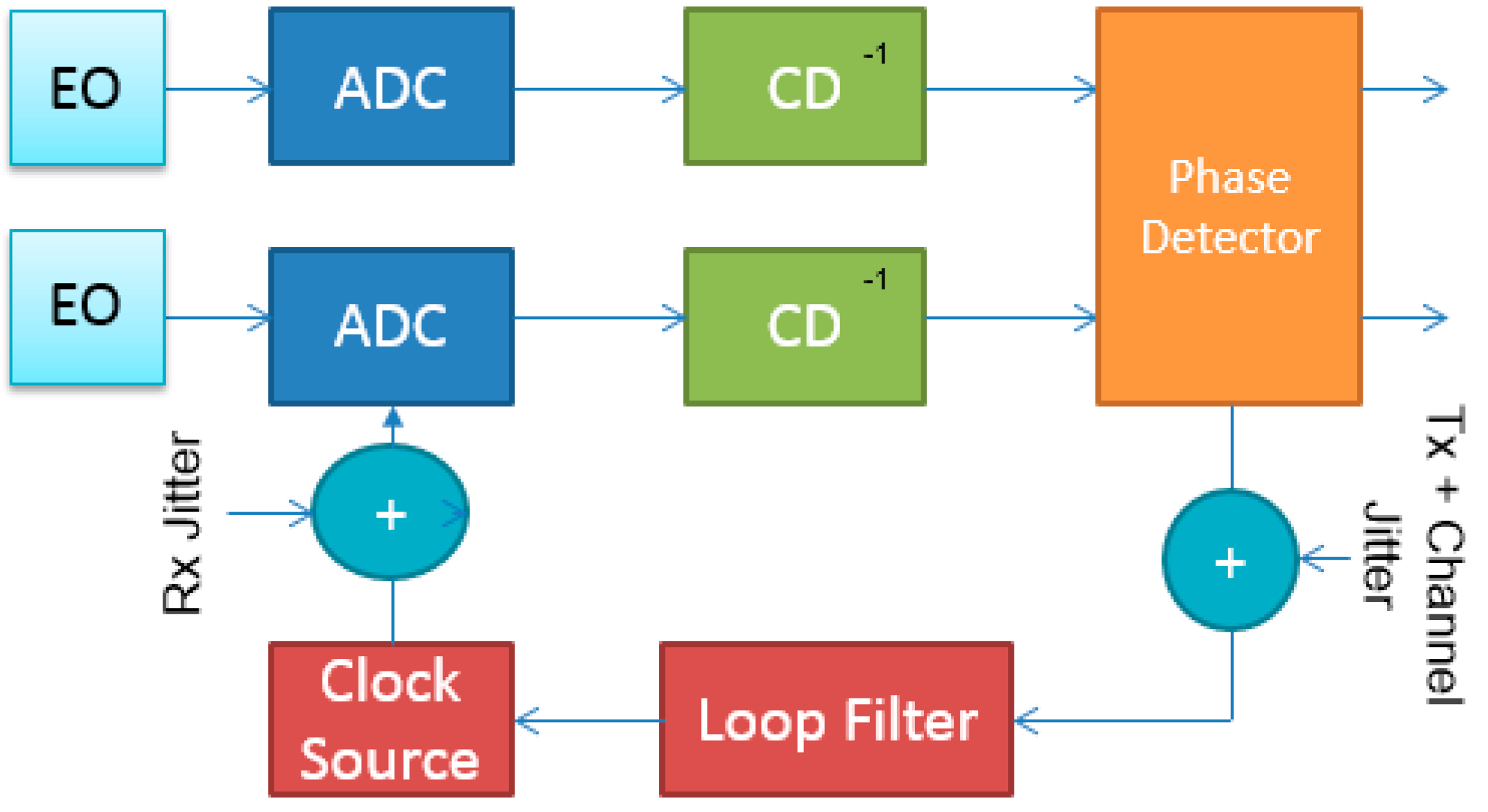
With rich modulation formats becoming the norm in coherent transceivers, data converters are more sensitive to degradations in signal-to-noise ratio (SNR); especially when single-carrier modems are used at high-baud rates. One way to maintain performance above required levels, and to allow signal processing to compensate for imperfections in the optical channel, is to reduce errors in clock synchronization for the ADC. The typical architecture of such apparatus is shown in Figure 2, in which the bulk CD is compensated for prior to PD. The error generated by the latter drives a filter that controls the frequency/phase of the ADC sampler. The main objective of the clock recovery is to estimate the timing offset and to compensate for it. The architectures discussed in the literature are typically a combination of digital and analog blocks, and designs can be feedforward-based, feedback, or a combination of both, and data-aided versus non-data-aided [16].
In the context of optical gridless networks, interference from adjacent channels is an extra source of linear impairment. It becomes a more difficult challenge when clock recovery depends on excess bandwidth, i.e., PD is non-data-aided. This is indeed the case in Nyquist and Super-Nyquist spacing. The latter is defined as when the spacing between channel and its neighbor (Δf) is smaller than the channel bandwidth (B). In the case of root-raised cosine pulse shaping, the excess bandwidth is governed by the roll-off factor β and T is the duration of the symbol and it is defined in time-domain as:
h ( t ) =   2 β π T cos [ ( 1 +   β ) n t T ] +   sin [ ( 1 β ) n t T ] 4 β t / T 1   ( 4 β t / T ) 2

2.1. Sources of Jitter

Coherent receivers must deal with two main sources of jitter, one is specific to optical impairments and the second is due to typical phase locked-loop (PLL) implementation. Jitter from optical links is due to itemized impairments below:
  • Amplified spontaneous emission (ASE) induced by optical line amplifiers can shift the pulse from its ideal location [17].
  • Kerr nonlinearity such as self-phase modulation (SPM) and cross-phase modulation (XPM) have effect on timing jitter as shown, respectively, in [18] and [19].
  • CD, which its bulk part should be compensated before being able to digitally recover timing information, although a certain residual dispersion tolerance is anticipated but it comes with a penalty. In [20], when CD is convoluted with the phase noise of the local oscillator it causes timing jitter.
From the electronics side or radio frequency (RF), on both the transmitter and receiver clocks, the dominant sources of jitter in PLLs are the VCO and charge pump (CP). With respect to the VCO, it is subject to jitter accumulation which manifests itself as high phase noise at low frequency offsets with respect to the carrier frequency. This can be expressed with the following simplified Leeson’ frequency domain equation [21]:
L ( f m ) = F K T e m p 2 P [ 1 f m 3 f c 2 f 1 f 4 Q L 2 + 1 f m 2 f c 2 Q L 2 + f 1 f f m + 1 ]
with:
  • Q: Resonator loaded QP: Resonator power
  • f 1 f : Flicker noise corner
  • f m : Offset from carrier
  • f c : RF frequency
  • F: Oscillator noise figure
  • K: Boltzmann’s constant
  • Temp: Temperature
Other sources of jitter, as listed in [22], are thermal noise, and flicker noise in clock buffers, internal aperture of the ADC, supply variation and electromagnetic coupling. The latter is due to the decrease in electronic channel lengths when circuits are integrated on the same substrate. Some jitter, or ripple effects, is caused by the closed-loop control. The design of the loop filter order and bandwidth plays a major role in controlling the total jitter induced.

2.2. PLL Basics

A detailed look at PLL, as shown in [23,24], allows us to elaborate on the limitations of the existing clock recovery architectures in optical modems. Both control theory and signal processing are required tools to study the stability of PLLs. The basic structure of PLL is depicted in Figure 3. A typical PLL consists of a PD, a low-pass loop filter (LPF) and a VCO in the feed-forward path and a frequency divider (NPLL) in the feedback path. The need for divider is that reference clocks, crystal-based ones, are stable and have low jitter at low frequencies. Therefore, we adjust the input voltage of the VCO as part of the feedback loop.
Under steady-state conditions, the PD creates an output that is proportional to the phase/frequency difference of its two inputs with a gain of Kp:
V e ( s ) =   K p   ( θ i ( s )   θ f ( s ) )
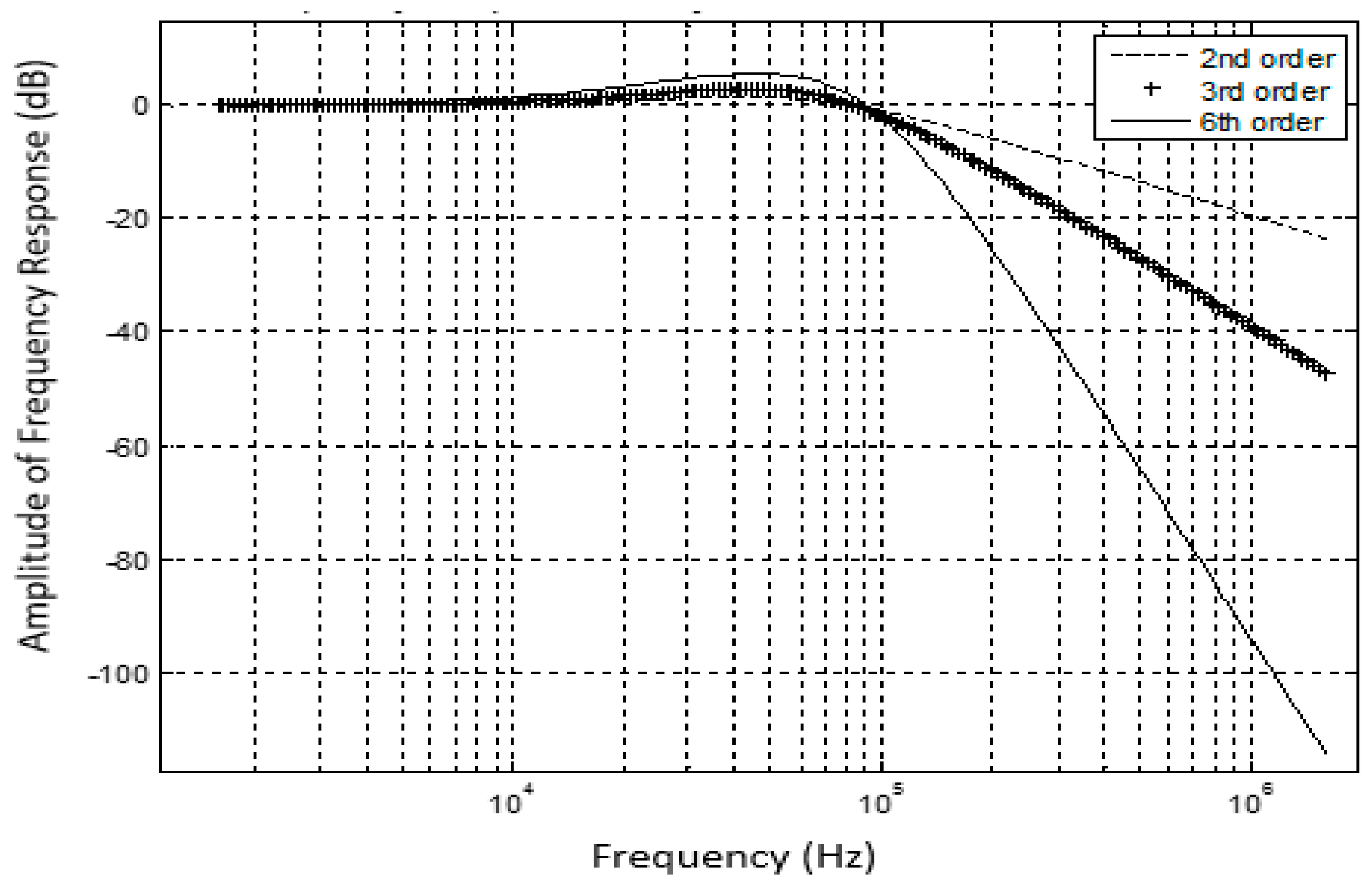
The loop filter (LPF) is assumed to be a low-pass filter with general transfer function F(s). The order of the filter depends on the configuration of the resistors (R) and capacitors (C). The higher the order of the PLL, the more rejection of high-frequency components is achieved in the forward path. If n is the number of cascaded resistor-capacitor (RC) stages, the resulting frequency domain filter response, have a roll-off of ( n x −20 dB)/decade. Figure 4 shows our simulation of the frequency response for a 2nd, 3rd, and 6th order PLL implementation. Filters of high orders achieve more rejection of noise and spurs from both VCO and reference.
The VCO is responsible for generating the high-frequency clock used to drive the ADC. It converts a voltage to frequency with a gain of KVCO and frequency offset w F R . Since the input and output variables of a PLL are best described in terms of instantaneous phase, the VCO operation can be described in the Laplace domain as:
θ o = K V C O s   V c ( s ) +   w F R s 2
Finally, the divider in the feedback path NPLL reduces the frequency or phase of the signal feedback to the PD:
θ f ( s ) =   θ o ( s ) N P L L
When deriving the closed-loop form reflecting input-output behavior of the PLL, we get an aggregation of a low-pass filter that governs the reference to output response and high-pass filter that governs the noise from the VCO viewed from the output. Presented in Equation (6) below:
θ o ( s ) θ i ( s ) = { N P L L W F R s ( N P L L s +   K V C O K p F ( s ) ) +   N P L L K V C O K p F ( s ) N P L L s 2 +   K V C O K p F ( s )   s   }
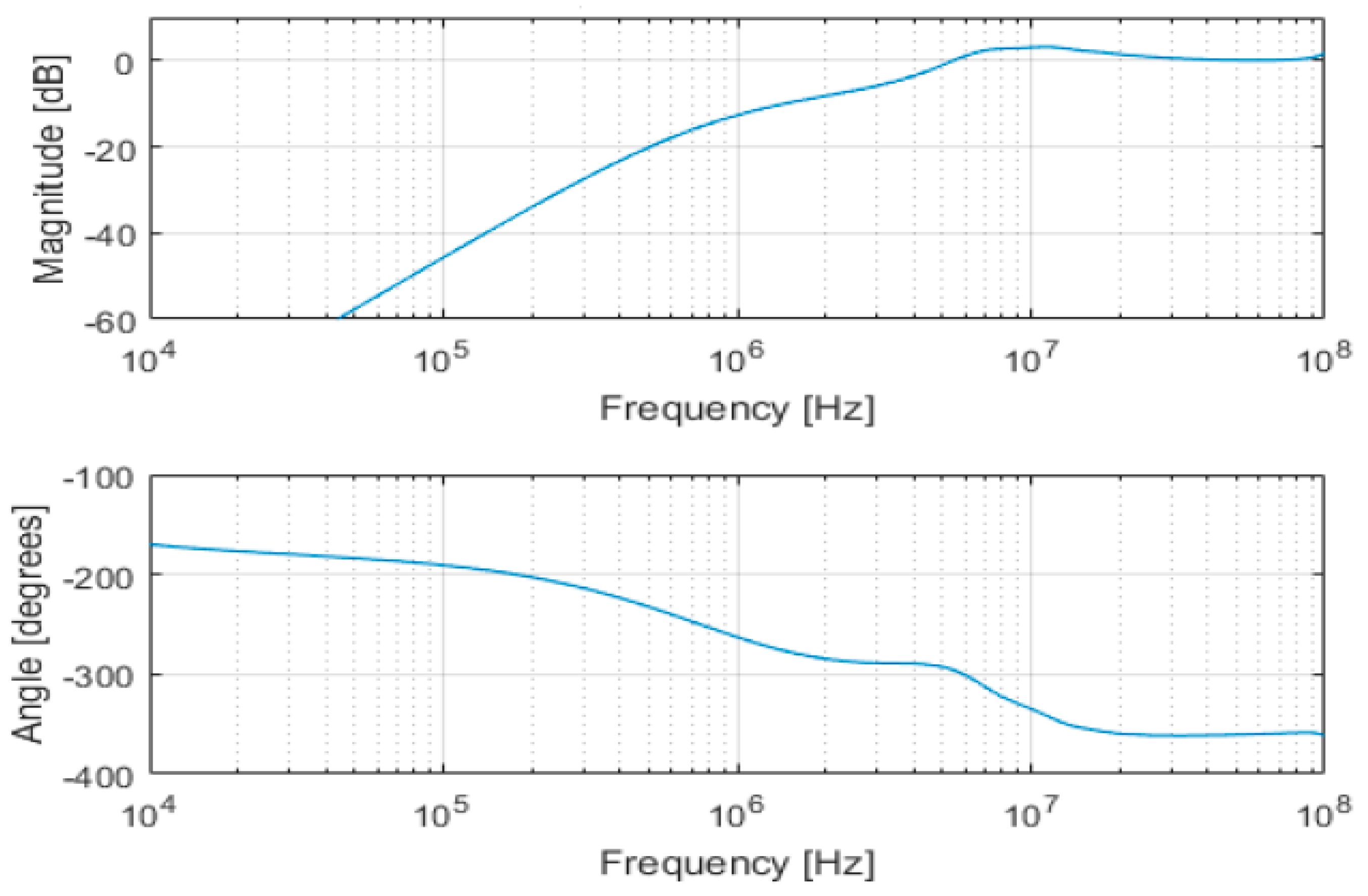
Typical reference clocks have their phase noise at low frequencies; Hence decreasing the forward-path loop bandwidth does not add much noise from the reference. However, decreasing bandwidth of the low-pass means increasing bandwidth of the complementary high-pass, shown in our simulation presented in Figure 5, and causing high-frequency VCO noise through unfiltered. This is a key ingredient in the optimization process discussed in the next section.

3. Proposed Clock Recovery Circuit and Method

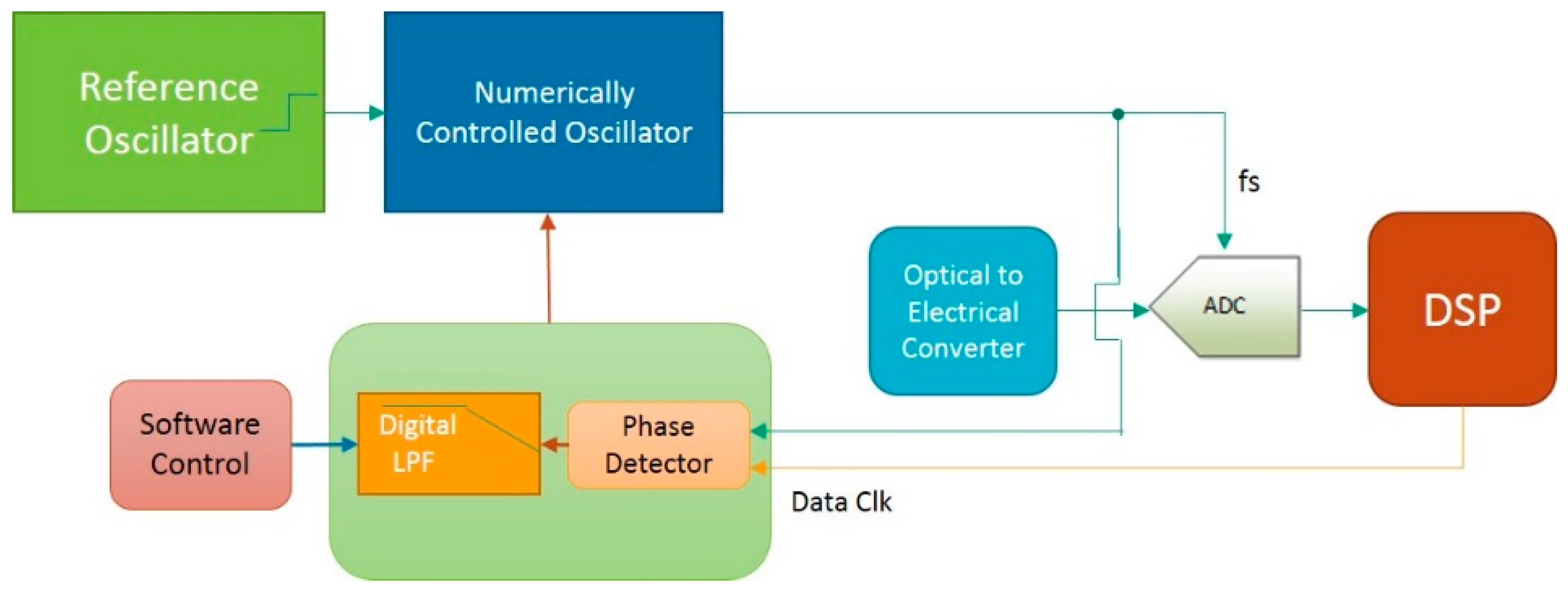
We are proposing a new methodology to optimize the channel spacing based on the total jitter seen by the receiver in gridless networks. As discussed in Section 2.2, when the timing recovery circuit is controlling the VCO directly, as in Figure 2, adjusting the loop bandwidth is limited by high-frequency noise injected by the VCO. Hence, the key limitation of existing clock recovery circuity is the lack of flexibility. In other words, the tracking bandwidth cannot be optimized when “Data Clk”, shown in Figure 6, is corrupted due to leaked power from neighboring channels. We propose a clock recovery architecture that overcomes this limitation. As well, we present a network level method, embedded in SDN ecosystem that allows for better spectrum efficiency compared to legacy methods.

3.1. Circuit

In the receiver, a clock recovery scheme which decouples the intrinsic VCO jitter bandwidth requirement from the clock recovery overall bandwidth is used. To do so, we are segregating our circuit into two loops: digital PLL, with high bandwidth in the forward path to filter as much as possible VCO noise, and another loop is governed by the software controlled “Digital LPF” and interacts with the “Numerically Controlled Oscillator” by adjusting phase delay. The architecture is presented in Figure 6. The parameters of the digital or analog PLL, represented as “Numerically Controlled Oscillator”, VCO gain/PD gain/loop damping and bandwidth are chosen in a way to guarantee a stable operation around the desired sampling frequency and adequate transient time.

3.2. Phase Detector

The second key component is the phase error detector at the Rx to estimate the jitter. It is worth noting that the method re-uses the circuits available in typical Rx for clock recovery (including jitter approximation) and BER/FER estimations. For the former method such as Gardener-based detector [26] can be used, where the timing error detected for the kth symbol is given by:
e ( k ) =   a I ( k ) +   a Q ( k )
where:
a I ( k ) = { y I ( ( k 1 ) T +   d k 1 )   y I ( k T +   d k ) } y I ( k T   T 2 +   d k 1 ) a Q ( k ) = { y Q ( ( k 1 ) T +   d k 1 )   y Q ( k T +   d k ) } y Q ( k T   T 2 +   d k 1 )
And T is the period of symbol, dk is the estimate of the phase at kT and yI and yQ are the received in-phase and quadrature components. τ0 corresponds to positive zero crossing point and the expectation is normalized to unit interval. In addition, jitter rms is estimated as where:
J i t t e r r m s =   1 T   { E [ e ( τ 0 ) 2 ] } 1 / 2 s l o p e ( τ 0 )
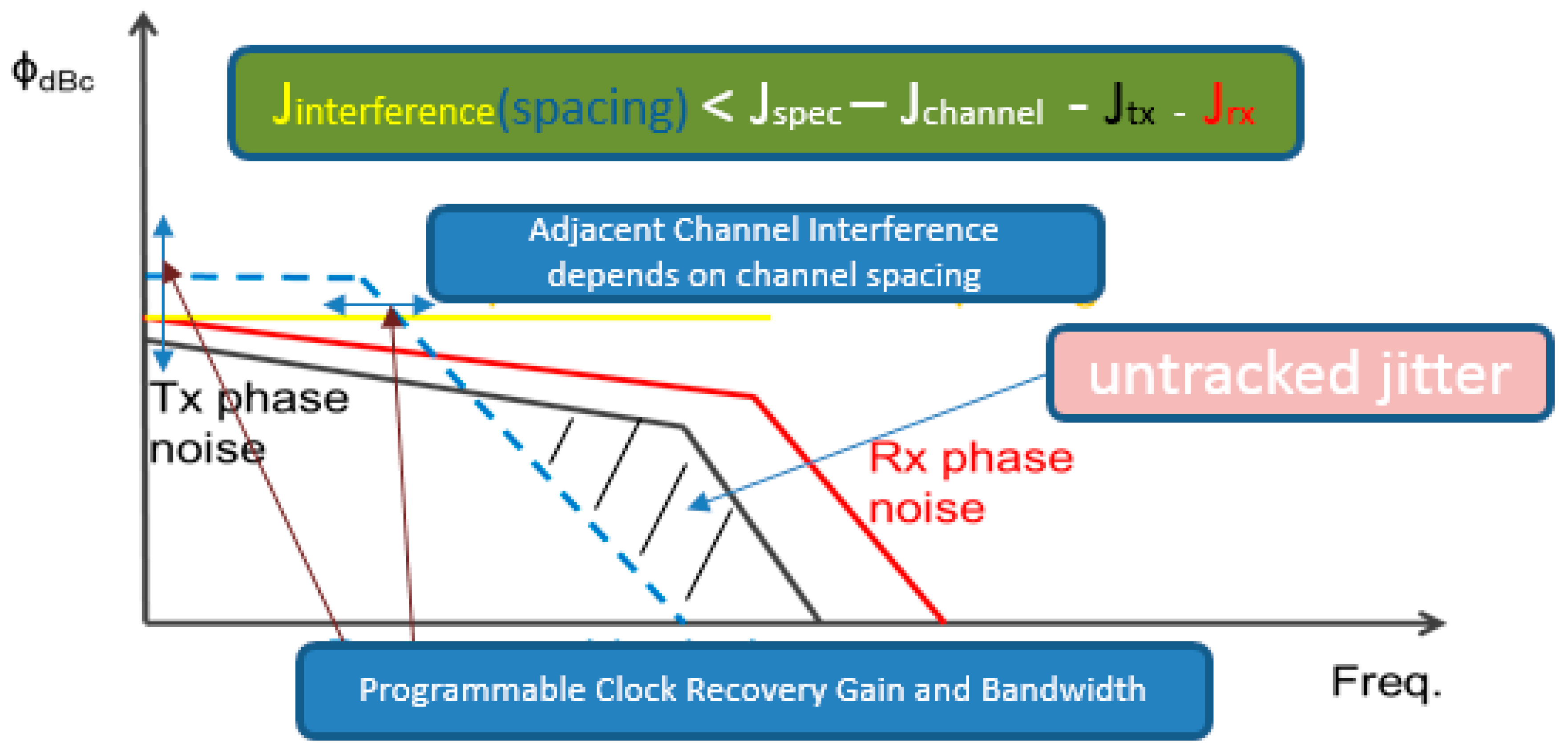
The phase-domain (ϕdBc) spectral density of the different contributors at the receiver is depicted in Figure 7. As can be seen, lowering the clock recovery bandwidth effectively helps in filtering out the impact of the adjacent channel interference (in yellow) and would provide better signal integrity with respect to the transmitter clock extraction. A scheme that takes into consideration phase noise induced by channel and where the effective clock recovery bandwidth and gain can be digitally programmed, to optimize the spacing, can be integrated into SDN framework.
To elaborate further, we note that when measuring SNR, and while noise is uncorrelated with zero mean, if the signal (phase error) is averaged over L observations the estimate is smoothed-out. That is the equivalent of lower loop’ bandwidth prior to producing a control signal. As we will see in the results, the system performance gets better if there is no high-frequency noise source that goes untracked. In addition, optimizing the clock recovery bandwidth reduces the effective tracking by the receiver of the other sources of jitter. As shown in Figure 7, we assume Jrx (jitter induced by Rx) is tracked by the receiver PLL and Jchannel can be estimated from neighboring channels in the same MC. For the cases of low transmitter clock standard deviation in the total phase error (Jtx), we can simply base the optimized parameters (bandwidth and gain) on the specification (i.e., targeted jitter to guarantee no guarantee no cycle slip in the ADC sampling) in order to perform a fitting to extract optimal channel spacing. The “Digital LPF”, shown in Figure 6, is implemented as simple proportional/integral control scheme, as in [27]. The higher the gain, the faster the loop reacts to changes. However, there is a trade-off between amounts of noise let through versus the agility in tracking higher frequency components.

3.3. Method Integrated in SDN Framework

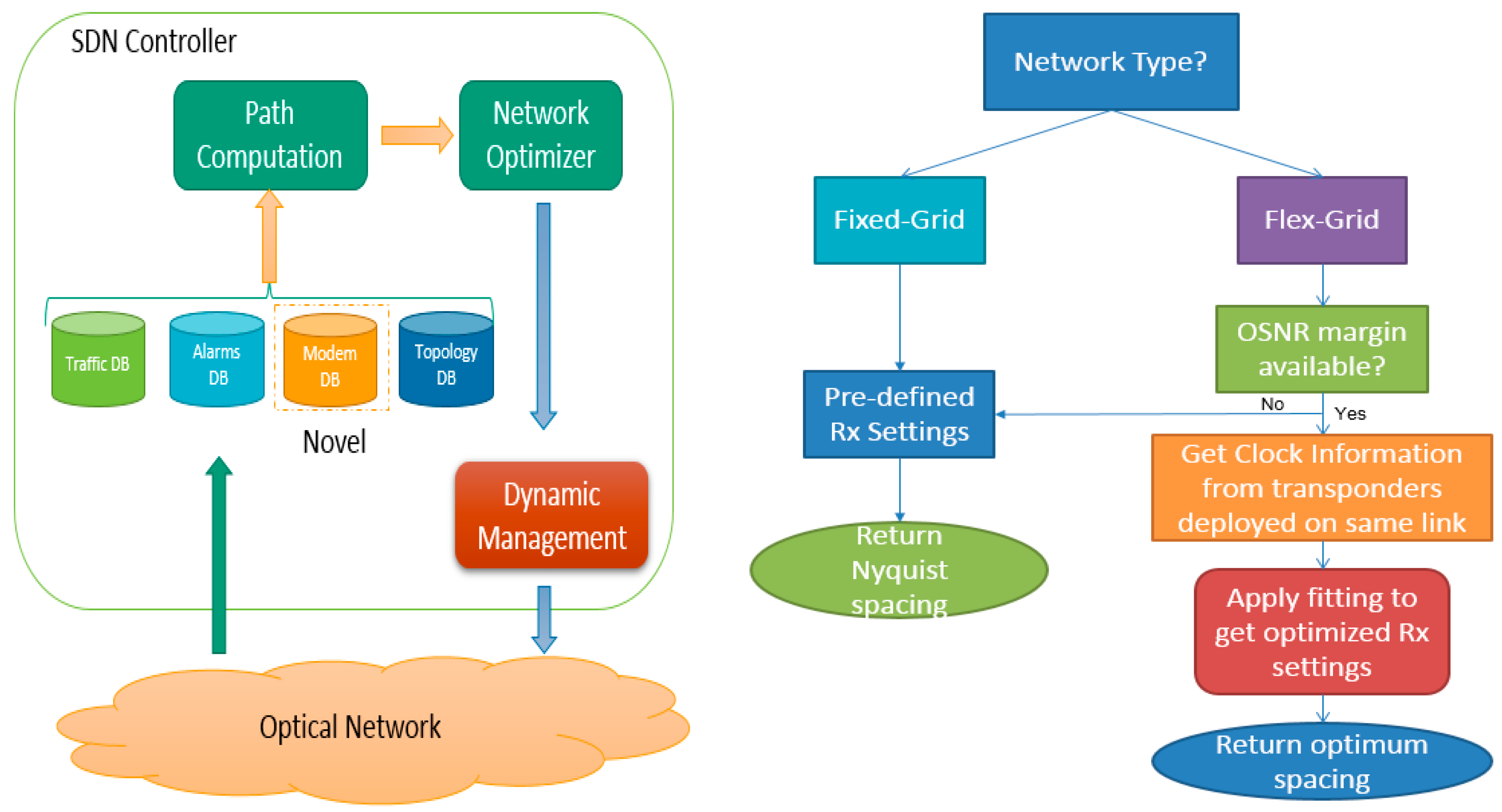
SDN offers a centralized server that oversees the whole network, it can aggregate information about the various links and modems. Industry standards such as Network Configuration Protocol (NETCONF), an Internet Engineering Task Force (IETF) network management protocol, is deployed to collect transponders configuration and measurements. Then software application will store relevant data in dedicated “Modem database” (DB), as illustrated in Figure 8, added to typical SDN controller. The “network optimizer” actor has a mechanism for viewing snapshots of available maximum concatenated capacity on each link group in the network. Moreover, a real-time view of the network can be supported to collect historical information to feed planning capacity needs and triggers for optimization activity. “Path Computation” process, along with up-to-date topology DB, allows for light-path establishment using a constrained-routing signaling protocol.
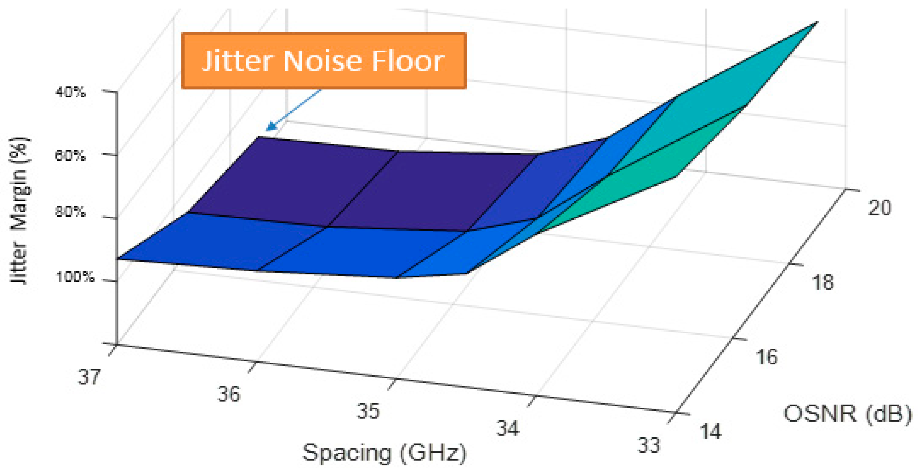
In the context of point-to-point DCI DWDM, such as 400ZR [28] aimed for link up to 120 Km (i.e., one span), nonlinearities of the fiber (such as SPM, FWM and XPM) have negligible role. A similar assumption applies to link OSNR specified to be at least 26 dB (due to the fact that only two Erbium-doped fiber amplifiers (EDFAs) are in the data-path of the optical signal), by Optical Internet Forum (OIF) standard in [28]; therefore, the spacing between the channels has the major role in determining the noise induced in the clock phase error estimation. For Fixed-Grid network configuration or when there is no OSNR margin in Flex-Grid link (beyond the required-OSNR of the modem), there is no room for optimizing spacing between channels; therefore, a pre-defined laser frequency (i.e., spacing) is communicated by the SDN controller to the transponder. The latter can be established using standardized data model such as the Yet Another Next Generation (YANG) model. On the other hand, upon a request for a new service in a Flex-Grid network and where OSNR margin is available (especially in the beginning of life of the modem), a brute force method can be used to optimize receiver parameters by adding the optical channel, i.e., activating the laser at the transmitter, at nominal spacing (pre-defined or at (1+β)*symbol-rate). Then run two-dimensional sweep for gain and bandwidth using receiver software/firmware to find the combination that achieves the minimal untracked jitter. If there is margin on untracked jitter, a fitting method, as shown in Figure 9, can be applied to determine the minimal spacing. Last, the SDN controller adjusts the laser frequency to squeeze the channel.

4. Experimental Results and Discussions

4.1. Experimental Setup

A set of experiments were conducted to get the quantitative benefits with real-world Flex-Grid settings using Ciena 6500 ROADMs. We used three 100G QPSK channels with the center one being the probe. Spacing, in GHz, is defined as the distance between the center of probe channel from the center of the interferer. We used the setup, shown in Figure 10, with three WaveLogic3 © transponders operating at 35 GBaud, two as interferers and one centered as the probe (i.e., “two neighbors”). Since most digital signal processing techniques for clock recovery are sensitive to optical impairments, our sweeps were done over multiple PDL, DGD, SOP scramblers (PC1 / PC2) and OSNR values. The latter is controlled by adjusting a VOA at the egress of an ASE source.

4.2. Results and Discussion

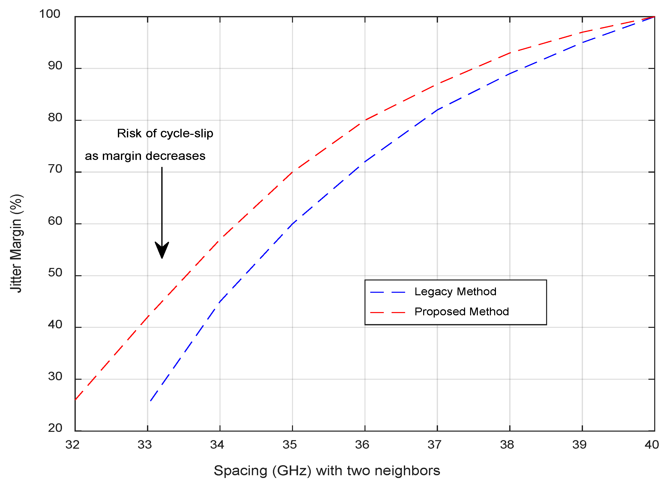
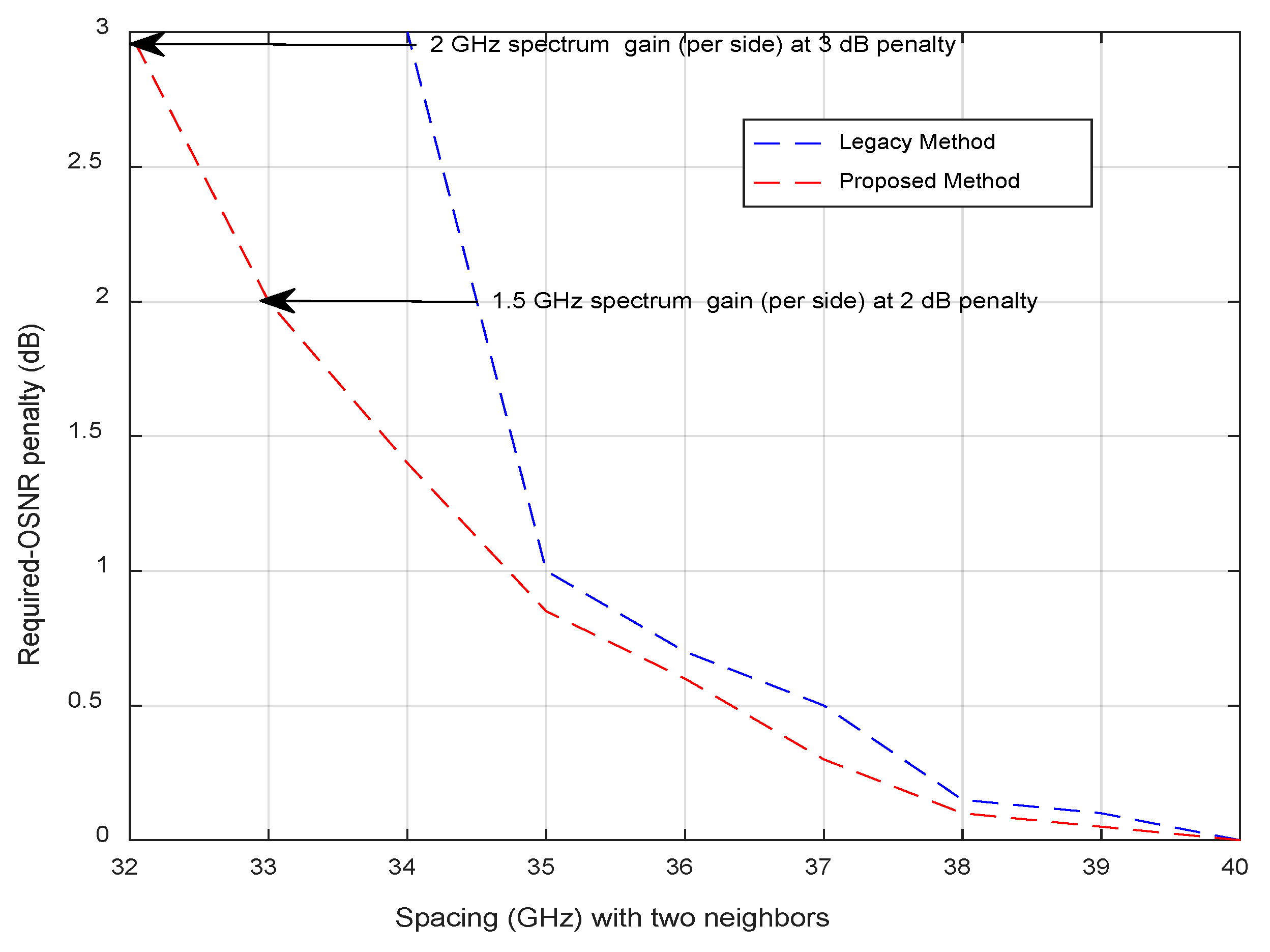
The results below are showing an experimental comparison versus the “state of the art”, labeled as “Legacy Method”, presented in [8]. Our test circuit, implemented in 28 nm complementary metal-oxide-semiconductor (CMOS) technology, has our new circuit and the typical architectures implemented. Under the exact same conditions, we compare the system level tolerance to channels spacing in gridless setup. We investigated both the SNR in steady state and cycle slip in acquisition state. When trying to reduce spacing between optical channels into the super-Nyquist mode of operation the penalty from linear crosstalk, which appears similar to white noise, is inevitable as discussed in [29]. Our method allows for pushing the bounds at which receiver can carry traffic. We were able to operate without any errors with the same 2 dB OSNR penalty as non-optimal method but with 1 GHz less spacing. In Figure 11, we show how the optimized method improves the jitter margin. “Legacy Method” is the optimization performed using circuits described in Figure 2. It has a fundamental limitation on the minimum filtering as it needs to reject the VCO high-frequency noise. In contrast, the main reason for extending the locking margin at the Rx is that we can filter the noise induced by channel, manifested by increased Jchannel, due to reducing the spacing below 40 GHz without being limited by Jrx as the two sources are decoupled in our new architecture.
We then show, in Figure 12, the system level benefit in terms of channel spacing with the associated OSNR penalty. The penalty from linear crosstalk is unavoidable; hence the increase in Required-OSNR penalty but it is shown that our method allows for tighter spacing, 1.5 GHz per size at 2 dB OSNR penalty, in a gridless setup.

5. Conclusions

We presented a novel circuit and method to optimize the channel spacing in gridless optical networks. We showed the results for 100G QPSK; however, the method was successfully tested for various data-rates/modulation formats (50G/BPSK and 200G/16QAM). When assuming 10 channels are propagating together in one MC, i.e., therefore there are nine spacings to be optimized, the experiment showed ability to gain from 13.5 GHz (9 × 1.5 GHz) for 2 dB OSNR margin and 18 GHz (9 × 2 GHz) for 3 dB OSNR margin in the optical spectrum. Typical optical links support 88 channels, therefore, 158.8 GHz is made available to be used to handle more services. It is expected that network providers assume at least 3 to 4 dB OSNR margin at early deployments to account for end-of-life degradation in modems and fiber aging. Our approach allows operators to take advantage of the margin to increase the capacity of their links and improve their return on investment (ROI). The method is generic and can be applied to other detectors, shown in [30], where edge frequencies are used as part of clock recovery.

6. Patents

US Patent App. 16/270,203: “Clock recovery circuits, systems and implementation for increased optical channel density”.

Author Contributions

A.A., S.A. and B.R. conceived the idea and performed simulations and measurements. N.B.-H. and C.D.A. analyzed the data and helped write the paper.

Funding

This work was partially funded by Natural Sciences and Engineering Research Council of Canada (NSERC) Grant #211300.

Conflicts of Interest

The authors declare no conflict of interest.

References

  1. Frisken, S.; Baxter, G.; Abakoumov, D.; Zhou, H.; Clarke, I.; Poole, S. Flexible and Grid-less Wavelength Selective Switch using LCOS Technology. In Proceedings of the 2011 Optical Fiber Communication Conference and Exposition and the National Fiber Optic Engineers Conference, Los Angeles, CA, USA, 6–10 March 2011. [Google Scholar] [CrossRef]
  2. Okoshi, T.; Kikuchi, K. Coherent Optical Communication Systems; KTK Scientific Publisher: Tokyo, Japan, 1988; Chapter 1. [Google Scholar]
  3. ITU. G.694.1: Spectral Grids for WDM Applications: DWDM Frequency Grid; ITU, 2012. Available online: https://www.itu.int/rec/T-REC-G.694.1-201202-I/en (accessed on 24 September 2019).
  4. Ben-Hamida, N.; Sitch, J.; Flemke, P.; Pollex, D.; Schvan, P.; Greshishchev, Y.; Wang, S.C.; Falt, C. Clock recovery for a 40 Gb/s QPSK optical receiver. In Proceedings of the 2009 16th IEEE International Conference on Electronics, Circuits and Systems (ICECS 2009), Yasmine Hammamet, Tunisia, 13–16 December 2009; pp. 695–698. [Google Scholar]
  5. Schuh, K.; Buchali, F.; Idler, W.; Hu, Q.; Templ, W.; Bielik, A.; Altenhain, L.; Langenhagen, H.; Rupeter, J.; Duemler, U.; et al. 100 GSa/s BiCMOS DAC Supporting 400 Gb/s Dual Channel Transmission. In Proceedings of the 42nd European Conference on Optical Communication (ECOC 2016), Dusseldorf, Germany, 18–22 September 2016; pp. 1–3. [Google Scholar]
  6. Zibar, D.; Bianciotto, A.; Wang, Z.; Napoli, A.; Spinnler, B. Analysis and dimensioning of fully digital clock recovery for 112 gb/s coherent polmux QPSK systems. In Proceedings of the 2009 35th European Conference on Optical Communication, Vienna, Austria, 20–24 September 2009; pp. 1–2. [Google Scholar]
  7. Hauske, F.N.; Stojanovic, N.; Xie, C.; Chen, M. Impact of optical channel distortions to digital timing recovery in digital coherent transmission systems. In Proceedings of the 2010 12th International Conference on Transparent Optical Networks, Munich, Germany, 27 June–1 July 2010; pp. 1–4. [Google Scholar]
  8. Stojanović, N.; Xie, C.; Zhao, Y.; Mao, B.; Gonzalez, N.G. A circuit enabling clock extraction in coherent receivers. In Proceedings of the 2012 38th European Conference and Exhibition on Optical Communications, Amsterdam, Netherlands, 16–20 September 2012; pp. 1–3. [Google Scholar]
  9. Diniz, J.C.M.; Piels, M.; Zibar, D. Performance Evaluation of Clock Recovery for Coherent Mode Division Multiplexed Systems. In Proceedings of the Optical Fiber Communication Conference, Los Angeles, CA, USA, 19–23 March 2017. [Google Scholar]
  10. Diniz, J.; Da Ros, F.; Zibar, D. Clock Recovery Challenges in DSP-Based Coherent Single-Mode and Multi-Mode Optical Systems. Future Internet 2018, 10, 59. [Google Scholar] [CrossRef]
  11. Stojanović, N.; Chuan, X. Clock recovery in coherent optical receivers. In Proceedings of the 2015 Optical Fiber Communications Conference and Exhibition (OFC), Los Angeles, CA, USA, 22–26 March 2015; pp. 1–3. [Google Scholar]
  12. Yan, M.; Tao, Z.; Dou, L.; Li, L.; Zhao, Y.; Hoshida, T.; Rasmussen, J.C. Digital clock recovery algorithm for Nyquist signal. In Proceedings of the 2013 Optical Fiber Communication Conference and Exposition and the National Fiber Optic Engineers Conference (OFC/NFOEC), Anaheim, CA, USA, 17–21 March 2013; pp. 1–3. [Google Scholar]
  13. Eramo, V.; Lavacca, F.G. Proposal and Investigation of a Reconfiguration Cost Aware Policy for Resource Allocation in Multi-Provider NFV Infrastructures Interconnected by Elastic Optical Networks. IEEE J. Light. Technol. 2019, 37, 4098–4114. [Google Scholar] [CrossRef]
  14. Eramo, V.; Lavacca, F.G. Optimizing the cloud resources, bandwidth and deployment costs in multi-providers network function virtualization environment. IEEE Access 2019, 7, 46898–46916. [Google Scholar] [CrossRef]
  15. Caria, M.; Jukan, A.; Hoffmann, M. A Performance Study of Network Migration to SDN-enabled Traffic Engineering. In Proceedings of the 2013 IEEE Global Communications Conference (Globecom 2013), Atlanta, GA, USA, 9–13 December 2013. [Google Scholar]
  16. Stojanović, N.; Zhao, Y.; Xie, C. Feed-forward and feedback timing recovery for Nyquist and faster than Nyquist systems. In Proceedings of the Optical Fiber Communication Conference 2014 (OFC 2014), San Francisco, CA, USA, 9–13 March 2014. [Google Scholar]
  17. Grigoryan, V.; Menyuk, C.; Mu, R.-M. Calculation of timing and amplitude jitter in dispersion-managed optical fiber communications using linearization. J. Light. Technol. 1999, 17, 1347–1356. [Google Scholar] [CrossRef]
  18. Eiselt, M.; Shtaif, M.; Garrett, L.D. Contribution of timing jitter and amplitude distortion to XPM system penalty in WDM systems. IEEE Photonics Technol. Lett. 1999, 11, 748–750. [Google Scholar] [CrossRef]
  19. Eiselt, M. The impact of non-linear fiber effects on fiber choice for ultimate transmission capacity. In Proceedings of the Optical Fiber Communication Conference 2000, Baltimore, MD, USA, 7 March 2000; Volume 1, pp. 58–60. [Google Scholar]
  20. Oda, S.; Ohshima, C.; Tanaka, T.; Tanimura, T.; Nakashima, H.; Koizumi, N.; Hoshida, T.; Zhang, H.; Tao, Z.; Rasmussen, J.C. Interplay between local oscillator phase noise and electrical chromatic dispersion compensation in digital coherent transmission system. In Proceedings of the 36th European Conference and Exhibition on Optical Communication, Torino, Italy, 19–23 September 2010; pp. 1–3. [Google Scholar]
  21. Leeson, D.B. A Simple Model of Feedback Oscillator Noise Spectrum. Proc. IEEE 1996, 54, 329–330. [Google Scholar] [CrossRef]
  22. Mehrotra, A. Noise analysis of phase-locked loops. IEEE Trans. Circuits Syst. I 2002, 49, 1309–1316. [Google Scholar] [CrossRef]
  23. Almeida, T.M.; Piedade, M.S. High performance analog and digital PLL design. In Proceedings of the 1999 IEEE International Symposium on Circuits and Systems VLSI (Cat. No.99CH36349), Orlando, FL, USA, 30 May–2 June 1999; Volume 4, pp. 394–397. [Google Scholar]
  24. Hsieh, G.C.; Hung, J.C. Phase-locked loop techniques—A survey. IEEE Trans. Ind. Electron. 1996, 43, 609–615. [Google Scholar] [CrossRef]
  25. Brownlee, M.; Hanumolu, P.K.; Mayaram, K.; Moon, U. A 0.5-GHz to 2.5-GHz PLL With Fully Differential Supply Regulated Tuning. IEEE J. Solid State Circuits 2006, 41, 2720–2728. [Google Scholar] [CrossRef]
  26. Gardner, F.M. A BPSK/QPSK timing-error detector for sampled receivers. IEEE Trans. Commun. 1986, 34, 423–429. [Google Scholar] [CrossRef]
  27. Wang, D.; Lu, K.; Rasmussen, P.O.; Yang, Z. Comparative study of low-pass filter and phase-locked loop type speed filters for sensorless control of AC drives. CES Trans. Electr. Mach. Syst. 2017, 1, 207–215. [Google Scholar]
  28. OIF 400ZR. Available online: https://www.oiforum.com/technical-work/hot-topics/400zr-2/ (accessed on 4 August 2019).
  29. Mehta, P.; Gaudette, J.; Li, J. Flexible grid spacing using Nyquist-shaped channels for undersea transmission. In Proceedings of the Photonics North 2014, International Society for Optics and Photonics, Montréal, QC, Canada, 28–30 May 2014. [Google Scholar]
  30. Huang, L.; Wang, D.; Lau, A.P.T.; Lu, C.; He, S. Performance analysis of blind timing phase estimators for digital coherent receivers. Opt. Express 2014, 22, 6749–6763. [Google Scholar] [CrossRef] [PubMed]
Figure 1. An example of gridless configuration.
Futureinternet 11 00206 g001
Figure 2. Simplified clock and data recovery schemes used in coherent receivers [8].
Futureinternet 11 00206 g002
Figure 3. Block diagram representation of a PLL (left) and third order PLL loop filter governing representing F(s) (right) ([25]).
Futureinternet 11 00206 g003
Figure 4. Frequency response of three PLLs with different filter order and same 3-dB bandwidth.
Futureinternet 11 00206 g004
Figure 5. VCO to output transfer functions.
Futureinternet 11 00206 g005
Figure 6. Clock recovery circuit used in proposed method.
Futureinternet 11 00206 g006
Figure 7. Phase-domain spectral density of different contributors.
Futureinternet 11 00206 g007
Figure 8. Model of SDN controller (left) and high-level flow of proposed method (right).
Futureinternet 11 00206 g008
Figure 9. Jitter margin as function of channel spacing and link OSNR.
Futureinternet 11 00206 g009
Figure 10. Experimental setup.
Futureinternet 11 00206 g010
Figure 11. Optimization of jitter through setting the proper tracking
Futureinternet 11 00206 g011
Figure 12. Results showing the advantage of the proposed optimization method
Futureinternet 11 00206 g012