
NBTI-Aware Transient Fault Rate Analysis Method for Logic Circuit Based on Probability Voltage Transfer Characteristics

Abstract
:1. Introduction
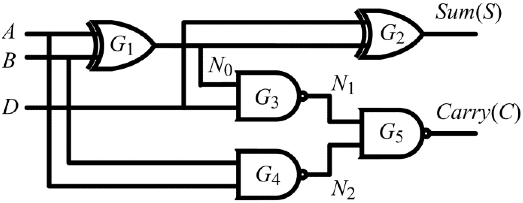
2. Methodology

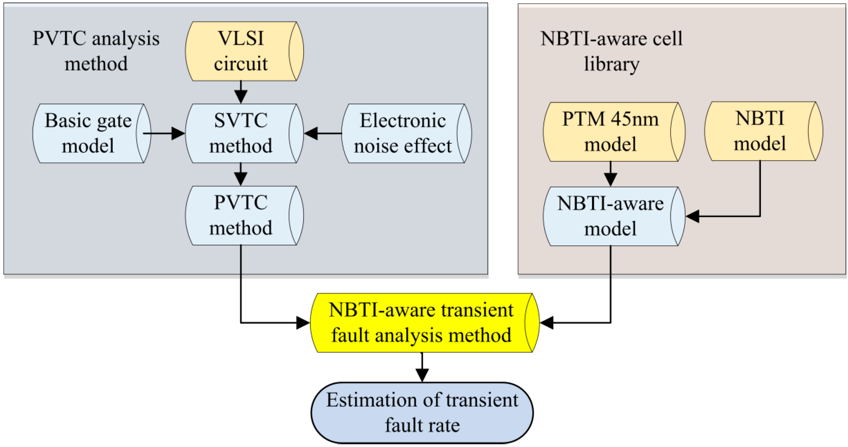
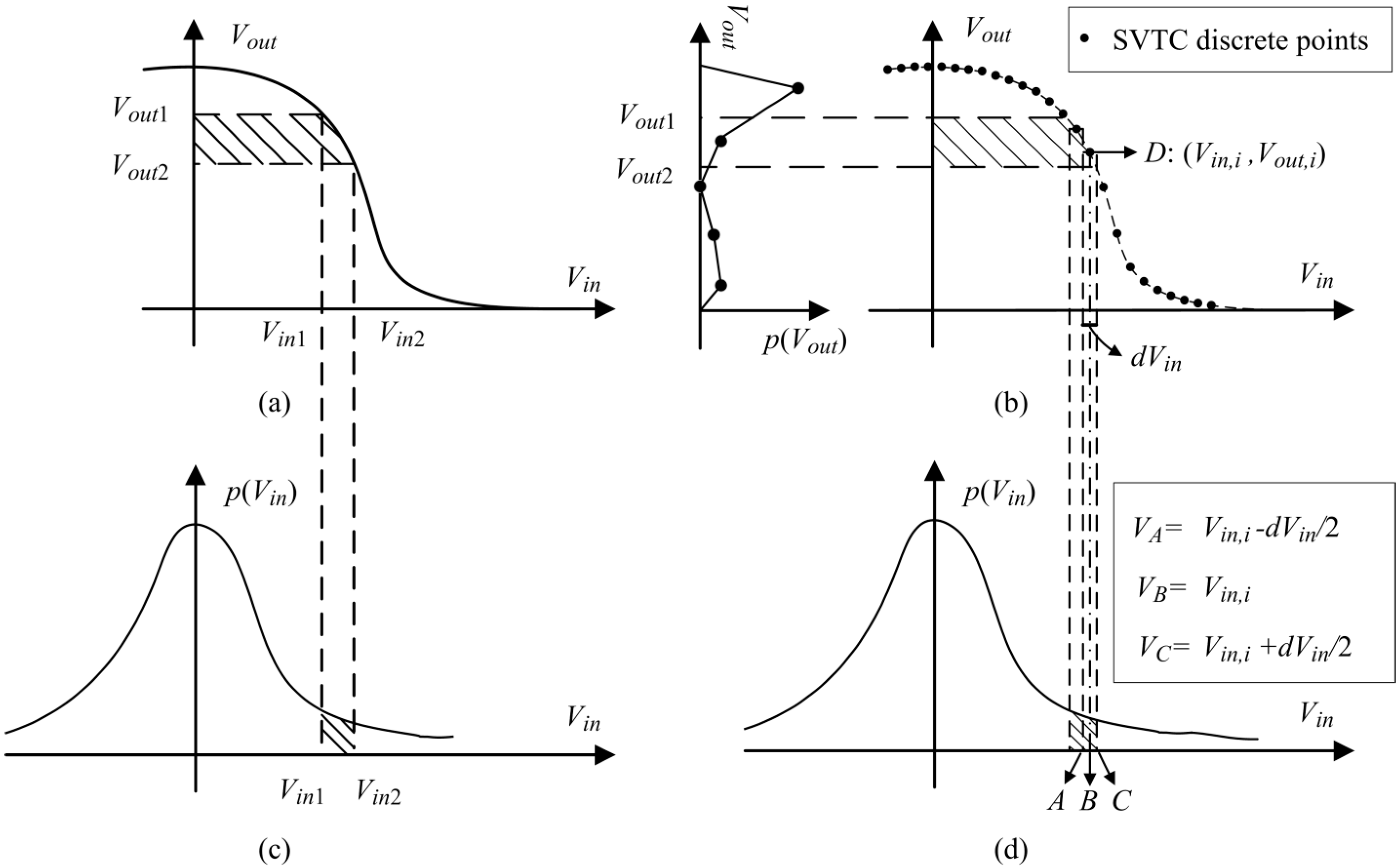
2.1. PVTC-Based Analysis for Single Logic Gates

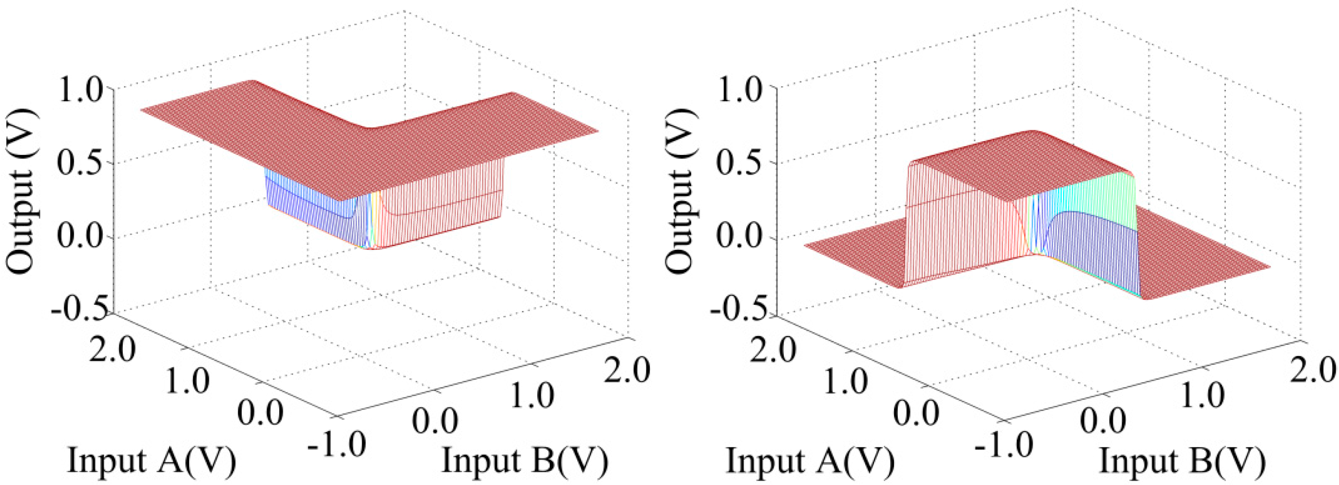
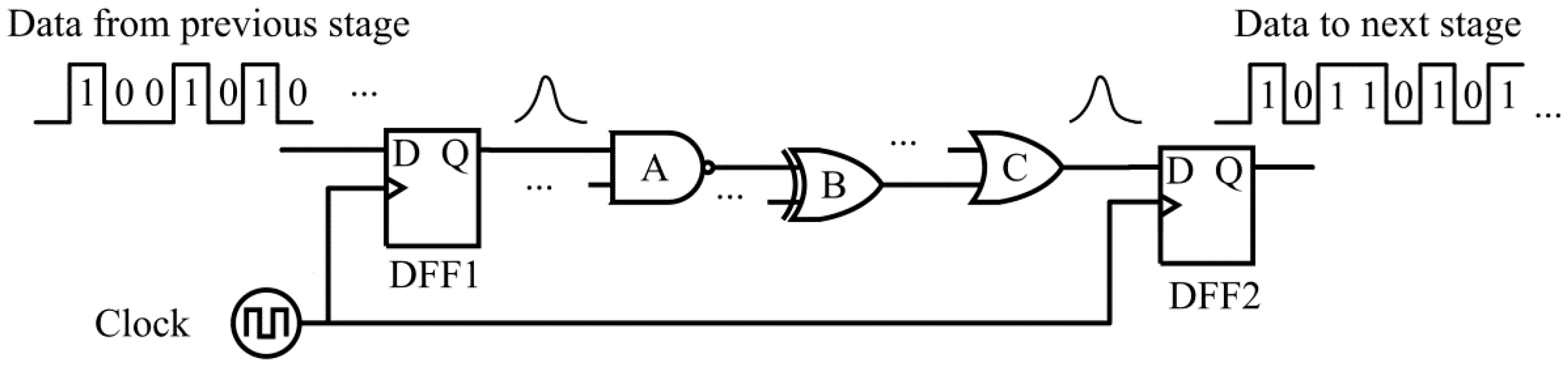
2.2. PVTC-Based Analysis for Multi-Gate Circuits
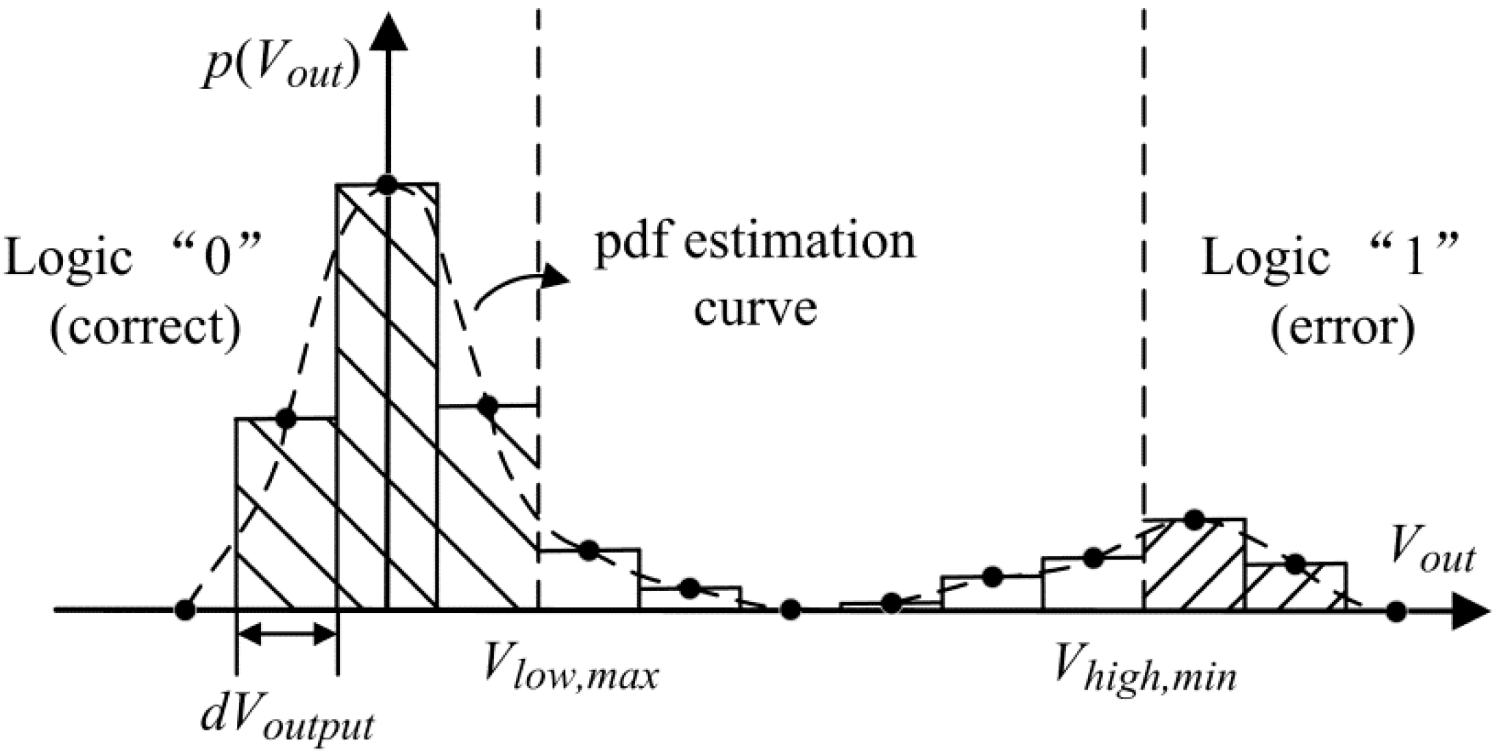
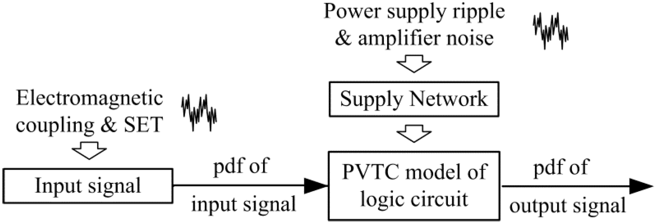
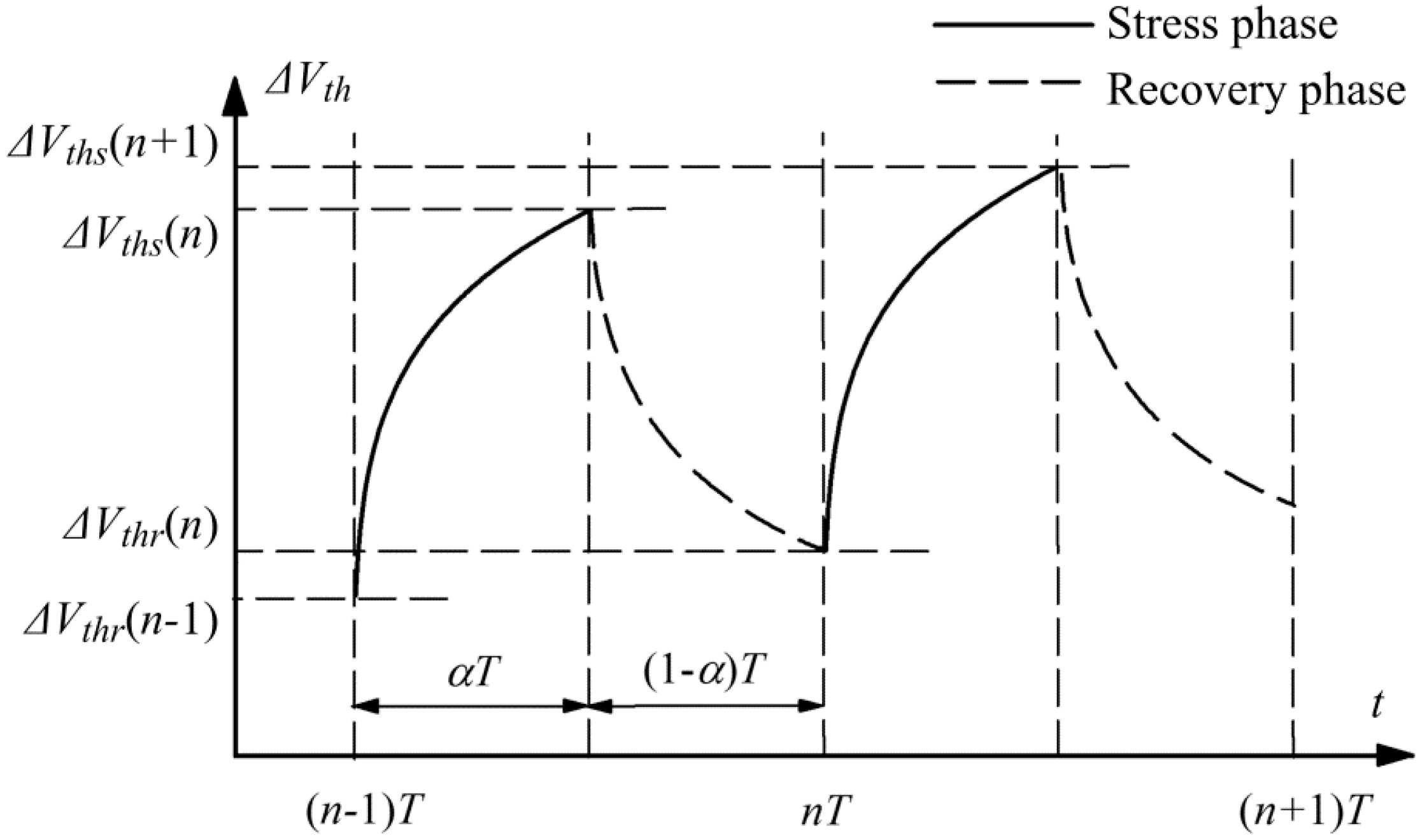
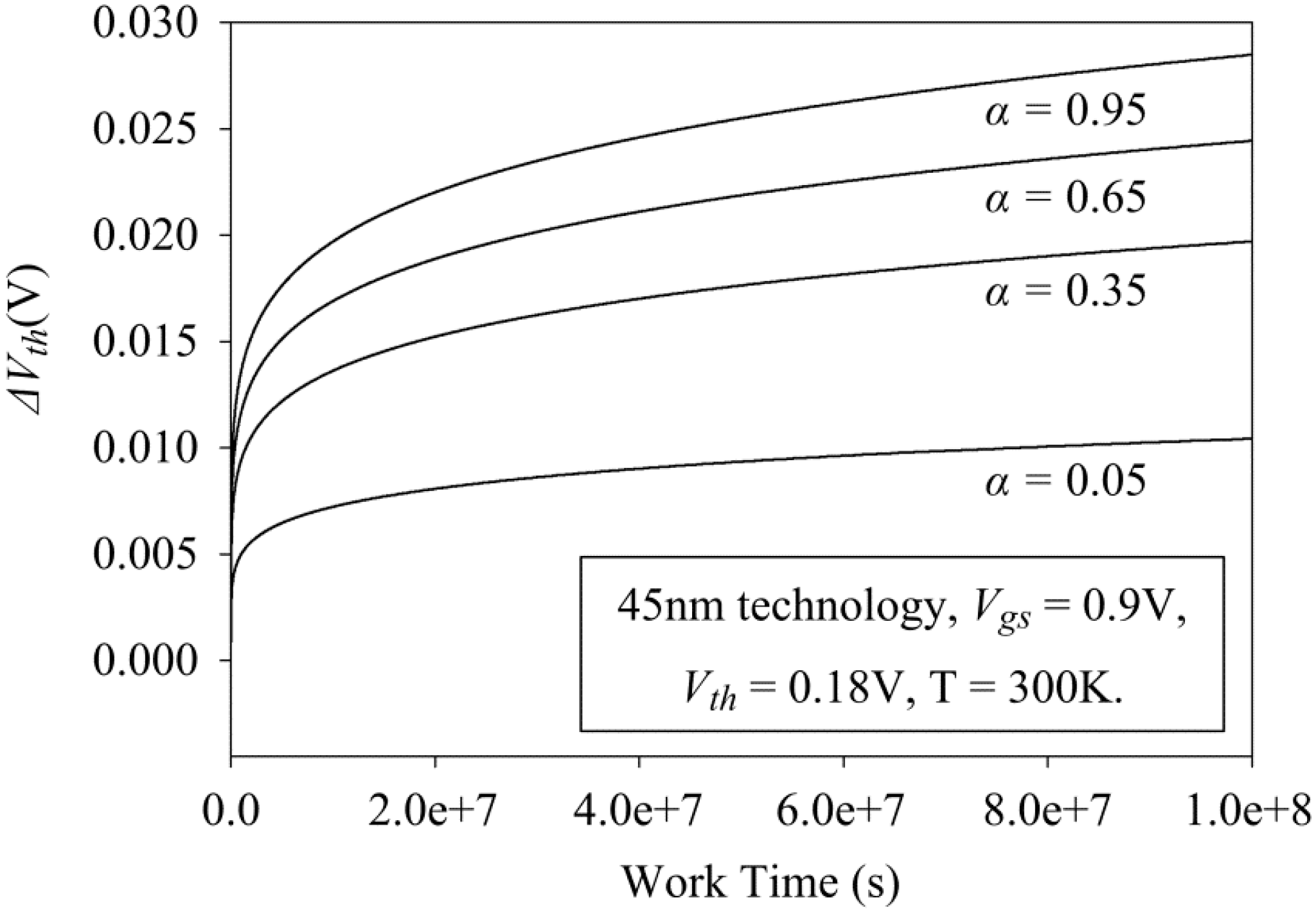
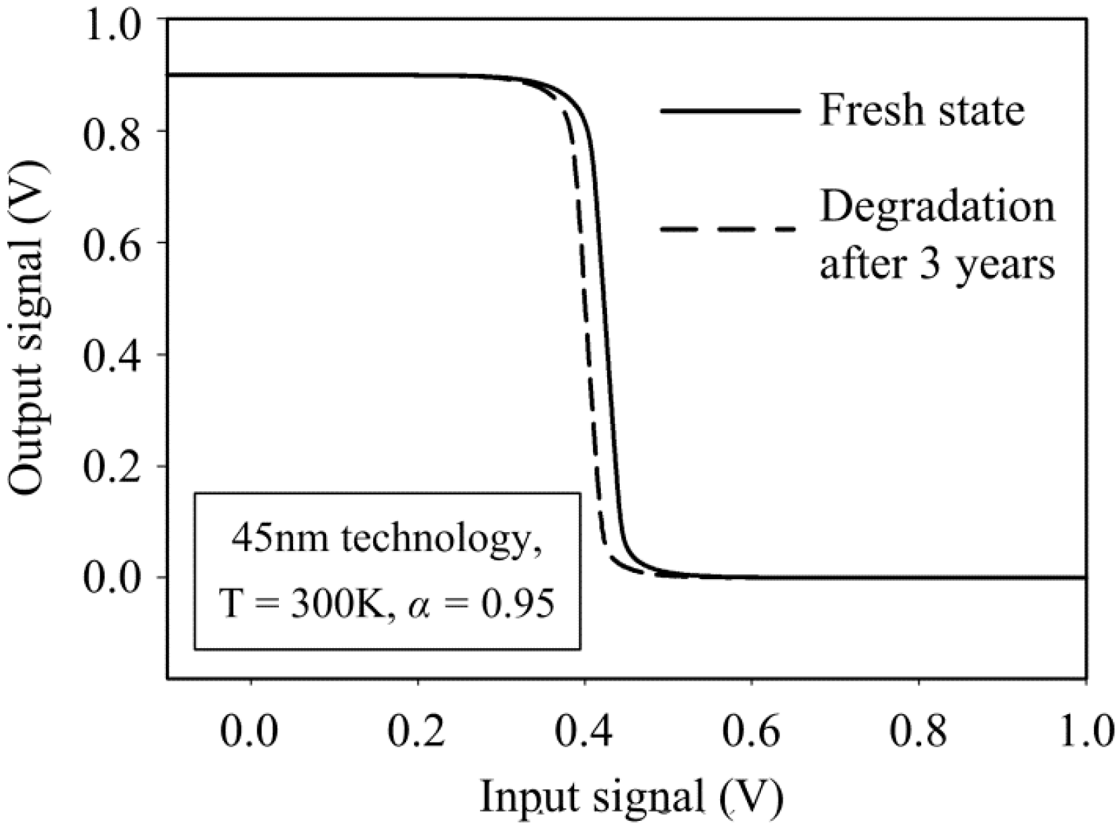
2.3. NBTI Effect and Its Impact on the PVTC Method


3. Results and Discussion
3.1. Experimental Setup
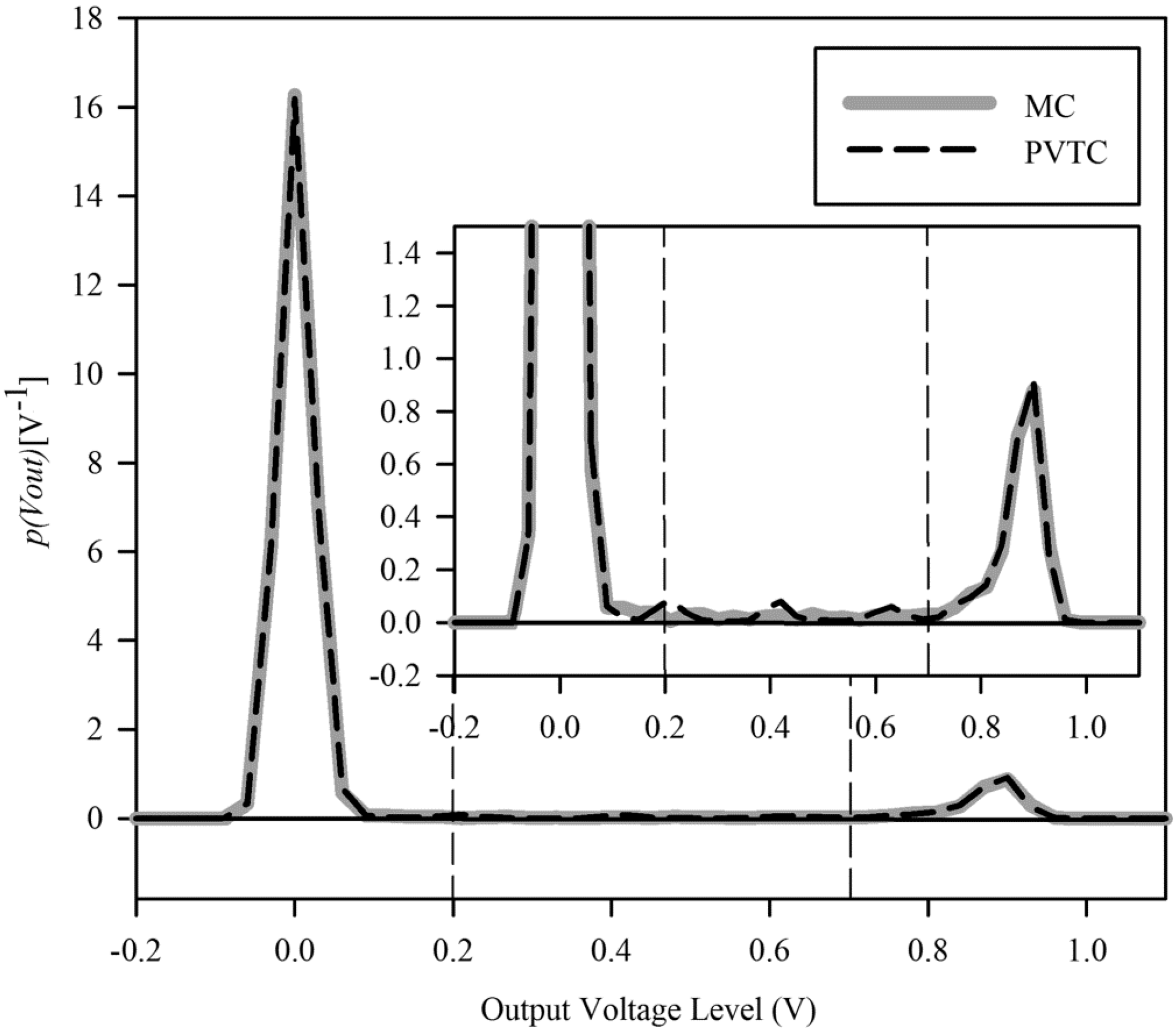
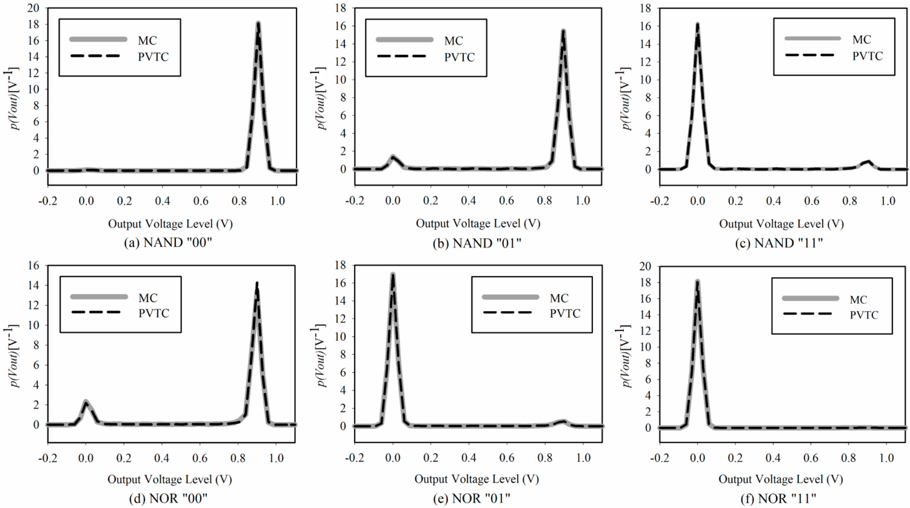
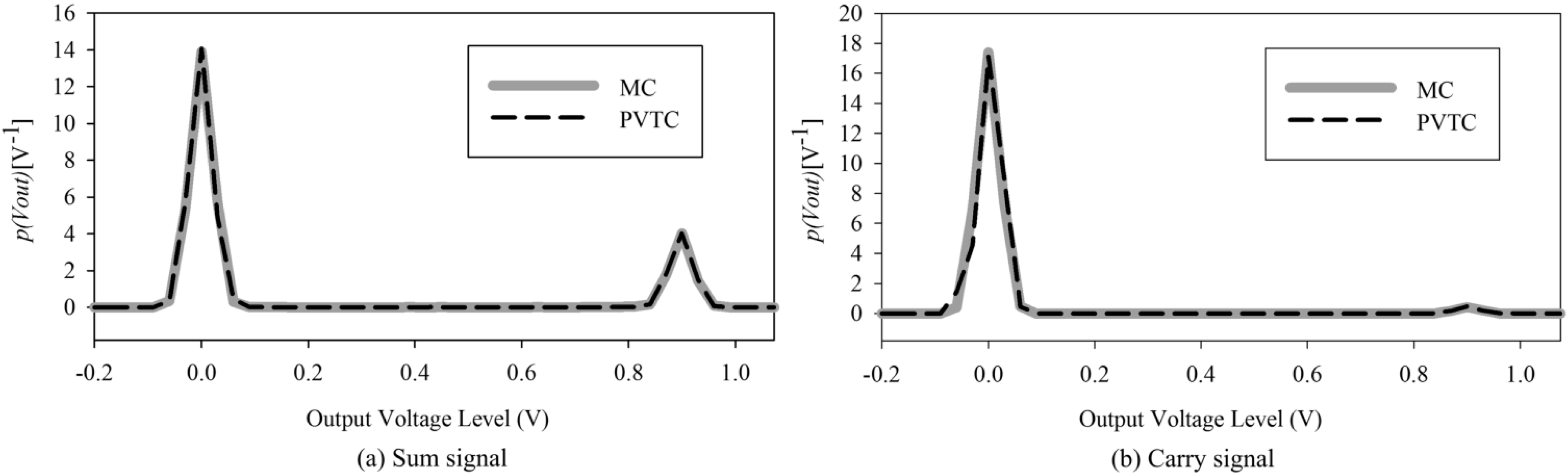
3.2. The PVTC Method for the Logic Circuit

| Logic Circuit | Input | Transient Fault Rate (%) | Error (%) | Runtime (s) | ||
|---|---|---|---|---|---|---|
| MC | PVTC | MC | PVTC | |||
| NAND Gate | 00 | 0.81 | 0.88 | 8.6 | 220 | 0.41 |
| 01 | 8.98 | 9.11 | 1.4 | |||
| 11 | 7.52 | 7.46 | −0.8 | |||
| NOR Gate | 00 | 15.47 | 14.80 | −4.3 | 230 | 0.39 |
| 01 | 4.77 | 4.41 | −7.5 | |||
| 11 | 0.23 | 0.21 | −8.7 | |||
| FA Sum | 000 | 22.71 | 22.88 | 0.7 | 452 | 1.0 |
| FA Carry | 000 | 2.57 | 2.55 | −0.8 | 452 | 1.8 |
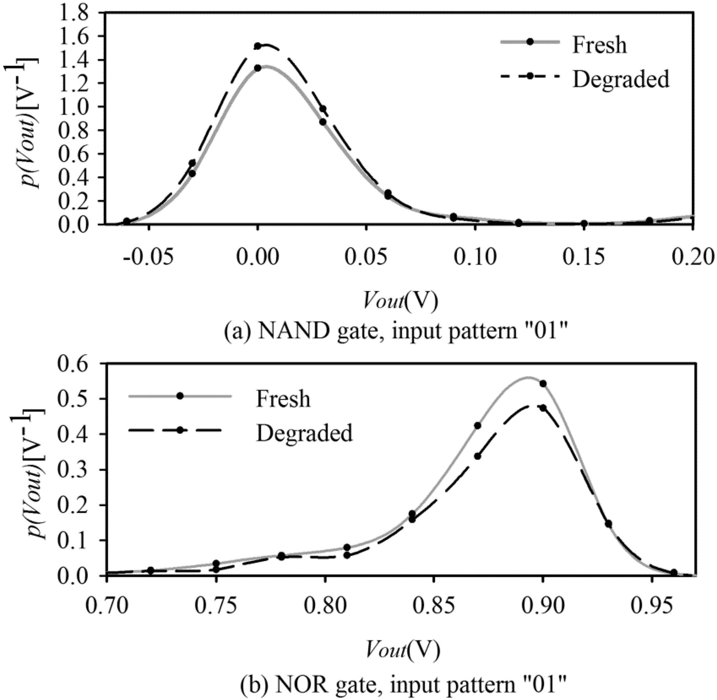
3.3. NBTI-Aware PVTC Method Analysis
| Logic Circuit | Input | Transient Fault Rate (%) | Change Rate (%) | |
|---|---|---|---|---|
| Fresh | Degraded | |||
| NAND Gate | 00 | 0.88 | 1.03 | +17.1 |
| 01 | 9.11 | 10.11 | +11.0 | |
| 11 | 7.46 | 6.51 | −12.7 | |
| NOR Gate | 00 | 14.80 | 16.89 | +14.1 |
| 01 | 4.41 | 3.78 | −14.3 | |
| 11 | 0.21 | 0.16 | −23.8 | |
| FA Sum | 000 | 22.88 | 25.11 | +9.8 |
| FA Carry | 000 | 2.55 | 3.22 | +26.3 |
4. Conclusions
Acknowledgments
Author Contributions
Conflicts of Interest
References
- Polian, I.; Hayes, J.P.; Reddy, S.M.; Becker, B. Modeling and mitigating transient errors in logic circuits. IEEE Trans. Dependable Secur. Comput. 2011, 8, 537–547. [Google Scholar] [CrossRef]
- Chang, A.C.C.; Huang, R.H.M.; Wen, C.H.P. Casser: A closed-form analysis framework for statistical soft error rate. IEEE Trans. Very Large Scale Integr. 2013, 21, 1837–1848. [Google Scholar] [CrossRef]
- Miskov-Zivanov, N.; Marculescu, D. Multiple transient faults in combinational and sequential circuits: A systematic approach. IEEE Trans. Comput. Aided Des. Integr. Circuits Syst. 2010, 29, 1614–1627. [Google Scholar] [CrossRef]
- Liu, X.; Zhang, Y.; Yuan, F.; Xu, Q. Layout-Aware Pseudo-Functional Testing for Critical Paths Considering Power Supply Noise Effects. In Proceedings of the Design, Automation and Test in Europe Conference and Exhibition, DATE 2010, Dresden, Germany, 8–12 March 2010; pp. 1432–1437.
- Ramanarayanan, R.; Degalahal, V.; Krishnan, R.; Kim, J.S.; Narayanan, V.; Xie, Y.; Irwin, M.J.; Unlu, K. Modeling soft errors at the device and logic levels for combinational circuits. IEEE Trans. Dependable Secur. Comput. 2009, 6, 202–216. [Google Scholar] [CrossRef]
- Zhou, Q.M.; Mohanram, K. Cost-Effective Radiation Hardening Technique for Combinational Logic. In Prorceedings of the 2004 IEEE/ACM International conference on Computer-aided design, San Jose, CA, USA, 7–11 November 2004; pp. 100–106.
- Zhou, Q.M.; Mohanram, K. Gate sizing to radiation harden combinational logic. IEEE Trans. Comput. Aided Des. Integr. Circuits Syst. 2006, 25, 155–166. [Google Scholar] [CrossRef]
- Mohanram, K.; Touba, N.A. Cost-Effective Approach for Reducing Soft Error Failure Rate in Logic Circuits. In Proceedings of the International Test Conference 2003, Charlotte, NC, USA, 30 September–2 October 2003; pp. 893–901.
- Kai-Chiang, W.; Marculescu, D. A low-cost, systematic methodology for soft error robustness of logic circuits. IEEE Trans. Very Large Scale Integr. Syst. 2013, 21, 367–379. [Google Scholar]
- Naseer, R.; Draper, J. DF-DICE: A Scalable Solution for Soft Error Tolerant Circuit Design. In Proceedings of the 2006 IEEE International Symposium on Circuits and Systems, Island of Kos, Greece, 21–24 May 2006; pp. 3890–3893.
- Shim, B.Y.; Sridhara, S.R.; Shanbhag, N.R. Reliable low-power digital signal processing via reduced precision redundancy. IEEE Trans. Very Large Scale Integr. 2004, 12, 497–510. [Google Scholar] [CrossRef]
- Wang, W.P.; Yang, S.Q.; Bhardwaj, S.; Vrudhula, S.; Liu, F.; Cao, Y. The impact of NBTI effect on combinational circuit: Modeling, simulation, and analysis. IEEE Trans. Very Large Scale Integr. 2010, 18, 173–183. [Google Scholar] [CrossRef]
- Huard, V.; Denais, M.; Parthasarathy, C. NBTI degradation: From physical mechanisms to modeling. Microelectron. Reliab. 2006, 46, 1–23. [Google Scholar] [CrossRef]
- Bhardwaj, S.; Wang, W.P.; Vattikonda, R.; Cao, Y.; Vrudhula, S. Predictive Modeling of the NBTI Effect for Reliable Design. In Proceedings of the Custom Integrated Circuits Conference, San Jose, CA, USA, 10–13 September 2006; pp. 189–192.
- Reddy, V.; Krishnan, A.T.; Marshall, A.; Rodriguez, J.; Natarajan, S.; Rost, T.; Krishnan, S. Impact of negative bias temperature instability on digital circuit reliability. Microelectron. Reliab. 2005, 45, 31–38. [Google Scholar] [CrossRef]
- Chopra, K.; Cheng, Z.; Blaauw, D.; Sylvester, D. Process Variability-Aware Transient Fault Modeling and Analysis. In Proceedings of the IEEE/ACM International Conference on Computer-Aided Design, 2008, ICCAD 2008, San Jose, CA, USA, 10–13 November 2008; pp. 685–690.
- Agarwal, A.; Chopra, K.; Blaauw, D.; Zolotov, V.; Soc, I.C. Circuit optimization using statistical static timing analysis. In Proceedings of the 42nd Design Automation Conference, Anaheim, CA, USA, 13–17 June 2005; pp. 321–324.
- Stathis, J.H.; Wang, M.; Zhao, K. Reliability of advanced high-k/metal-gate n-FET devices. Microelectron. Reliab. 2010, 50, 1199–1202. [Google Scholar] [CrossRef]
- Schleifer, J.; Coenen, T.; Noll, T.G. Statistical modeling of reliability in logic devices. Microelectron. Reliab. 2011, 51, 1469–1473. [Google Scholar] [CrossRef]
- Huang, H.M.; Wen, C.H.P. Fast-yet-accurate statistical soft-error-rate analysis considering full-spectrum charge collection. IEEE Des. Test 2013, 30, 77–86. [Google Scholar] [CrossRef]
- Grasser, T.; Kaczer, B.; Goes, W.; Reisinger, H.; Aichinger, T.; Hehenberger, P.; Wagner, P.J.; Schanovsky, F.; Franco, J.; Luque, M.T.; et al. The paradigm shift in understanding the bias temperature instability: From reaction-diffusion to switching oxide traps. IEEE Trans. Electron Devices 2011, 58, 3652–3666. [Google Scholar] [CrossRef]
- Zhao, W.; Cao, Y. New Generation of Predictive Technology Model for Sub-45 nm Design Exploration; IEEE Computer Soc: Los Alamitos, CA, USA, 2006; pp. 585–590. [Google Scholar]
- Agarwal, M.; Balakrishnan, V.; Bhuyan, A.; Kim, K.; Paul, B.C.; Wang, W.P.; Yang, B.; Cao, Y.; Mitra, S.; Society, I.C. Optimized Circuit Failure Prediction for Aging: Practicality and Promise. In Proceedings of the 2008 IEEE International Test Conference, Santa Clara, CA, USA, 28–30 October 2008; IEEE Computer Soc: Los Alamitos, CA, USA, 2008; pp. 656–665. [Google Scholar]
© 2016 by the authors; licensee MDPI, Basel, Switzerland. This article is an open access article distributed under the terms and conditions of the Creative Commons by Attribution (CC-BY) license (http://creativecommons.org/licenses/by/4.0/).
Share and Cite
Yang, Z.; Li, J.; Yu, Y.; Peng, X. NBTI-Aware Transient Fault Rate Analysis Method for Logic Circuit Based on Probability Voltage Transfer Characteristics. Algorithms 2016, 9, 9. https://doi.org/10.3390/a9010009
Yang Z, Li J, Yu Y, Peng X. NBTI-Aware Transient Fault Rate Analysis Method for Logic Circuit Based on Probability Voltage Transfer Characteristics. Algorithms. 2016; 9(1):9. https://doi.org/10.3390/a9010009
Chicago/Turabian StyleYang, Zhiming, Junbao Li, Yang Yu, and Xiyuan Peng. 2016. "NBTI-Aware Transient Fault Rate Analysis Method for Logic Circuit Based on Probability Voltage Transfer Characteristics" Algorithms 9, no. 1: 9. https://doi.org/10.3390/a9010009
APA StyleYang, Z., Li, J., Yu, Y., & Peng, X. (2016). NBTI-Aware Transient Fault Rate Analysis Method for Logic Circuit Based on Probability Voltage Transfer Characteristics. Algorithms, 9(1), 9. https://doi.org/10.3390/a9010009