1. Introduction
Recently, smart energy environments have gained significant attention due to their rapid development. When an electronic device is subjected to an electromagnetic (EM) field, a phenomenon known as electromagnetic interference (EMI) may take place. Any equipment with electrical circuitry is highly exposed to EMI [
1,
2,
3,
4]. In other words, the EMI is defined as the disruption to an electrical circuit caused by electromagnetic induction or externally released electromagnetic radiation. Also, it gains greater attention as the electromagnetic spectrum is being used more and more, and as electronic devices get more advanced and complex. EMI can be caused by a variety of natural or artificial factors. Depending on its source and the type of mechanism causing the interference, it may also have a range of properties. Electromagnetic interference (EMI) is the condition where undesired electromagnetic emissions of one electrical system interfere with other equipment nearby. The emissions usually result from components or systems having alternating currents or switching voltages rapidly, such as switching power supplies, motor drives, or digital electronics. The EMI-induced interference degrades the function, accuracy, or even safety of the surrounding electronic systems within the same setting. One must understand the path EMI travels from the source to the offending receiver to effectively mitigate. The interference path is referred to as “coupling” and may be accomplished by numerous different mechanisms, such as radiated, conducted, capacitive, or inductive coupling. These coupling mechanisms present some difficulties and require various methods of suppression. Therefore, an accurate definition of the coupling path is essential to ascertain the right amount of shielding, grounding, filtering, or modification of the circuit configuration to mute or eliminate the EMI’s interference effect on other devices.
For EMS within the broad context of electromagnetic interference (EMI) and electromagnetic compatibility (EMC in the specialized domain, some highly specific and domain-specific facts are of the highest significance when designing dependable and interference-immune electronic systems. One interesting fact is that the EMS encompasses all frequencies of electromagnetic radiation, from very low frequencies (VLF) to gamma rays, but when discussing EMI, the focus primarily remains between the radio frequency (RF) ranges, often a few kHz to several GHz. In this frequency band, electronic circuits and components inadvertently emit interference signals that radiate or propagate interference signals and impair the neighboring or connected system performance. Correct spectral management with proper assignment and monitoring of the frequencies to prevent overlap and inadvertent coupling between operating in the same frequency bands becomes essential. Equipment should be made to be able to function in their assigned spectral space and to attenuate outside-of-space emissions so that they can co-exist with other electronic devices.
Another EMS-specific aspect is the coupling mechanism by which EMI propagates from the source to victim. The coupling mechanisms are categorized into four main types: radiated, conducted, capacitive, and inductive. In EMS, one needs to know how energy couples—either by air as radiated fields or by contact as conducted signals—to design mitigation schemes. For instance, radiated coupling prevails when the source-to-victim distance is more than a wavelength, and one has to employ shielding enclosures and absorber materials. Directed EMI, on the other hand, is noise that propagates over cables and power lines and needs to be removed by low-pass filters or common-mode chokes. Such a detailed understanding of the way the interference travels and acts in the EMS environment enables engineers to implement specific countermeasures and improve overall system immunity.
Compliance with EMC standards worldwide is also an EMS-centric fact of special significance. These comprise regulations for allowed levels of emissions as well as immunity standards that systems should comply with so that they can work as expected under the effects of EMI. Such products cannot be lawfully marketed or used, especially in safety-critical applications like aerospace, defense, and healthcare, where EMS management is an important aspect of safety and performance. Hence, prudent pre-compliance and post-compliance EMC testing in anechoic or semi-anechoic chambers is a part of the product design process in the EMS field so that electromagnetic behavior will still comply with international standards and functional requirements.
Among numerous ways electromagnetic interference propagates from a source into a vulnerable victim circuit, conducted and radiated EMI are two principal and most popularly categorized forms. In order to design effective electromagnetic compatibility (EMC) solutions in electronic hardware, one should understand the behavior and differences between the two coupling methods. Radiated EMI is the electromagnetic interference that propagates through free space as electromagnetic waves. Such a type of coupling is normally predominant when the interfering source and victim device (or victim) are more than a wavelength apart from each other at the signal frequency. In this situation, the source is basically behaving as an antenna, radiating electromagnetic energy into the environment unintentionally. The victim subsequently behaves as a receive antenna that captures this radiated signal, which is potentially unwanted and can lead to malfunction or degradation of performance. This undesired energy can be from deliberate radiators like transmitters or unintentional radiators like switching power supplies, digital logic, or motors emitting high-frequency noise. Radiated EMI is harder to combat since it doesn’t need an electric path between the victim and source, but rather uses electromagnetic field propagation in space. The energy may couple into the victim’s circuitry through a wide range of mediums like cables, PCB traces, or enclosure openings, so shielding and good PCB layout are fundamental defense techniques. Radiated EMI is normally treated by engineers using techniques like putting sensitive parts in metal shielding, reducing loop areas in circuit layout, differential signaling, and employing good filtering and grounding techniques. This kind of interference is particularly crucial in high-frequency equipment systems, wireless communications, and densely grouped equipment environments which are electrically isolated, and where radiated EMI will need to be addressed as soon as possible within the design.
Conducted EMI: As the name suggests, conducted emissions happen when signals can travel along a conduction path. Power cables or other connectivity cabling might be present here. There are two possible modes for the conduction:
Common mode: This kind of EMI coupling happens when the noise is present on both conductors at the same time, such as the out and return conductors for communications or the positive/negative conductors for power connections.
Differential mode: This happens when the noise on the two conductors is out of phase.
In the conventional works, there are different types of EMI reduction methodologies [
5,
6,
7] have been developed to improve the overall system performance. The major categories of EMI reduction methodologies [
8,
9] are shown in
Figure 1.
Most existing works mainly use random and deterministic modulation techniques [
4,
10,
11] along with DC–DC converter topology to mitigate the level of EMI noise. When compared to the deterministic modulation techniques, the random modulation techniques [
12,
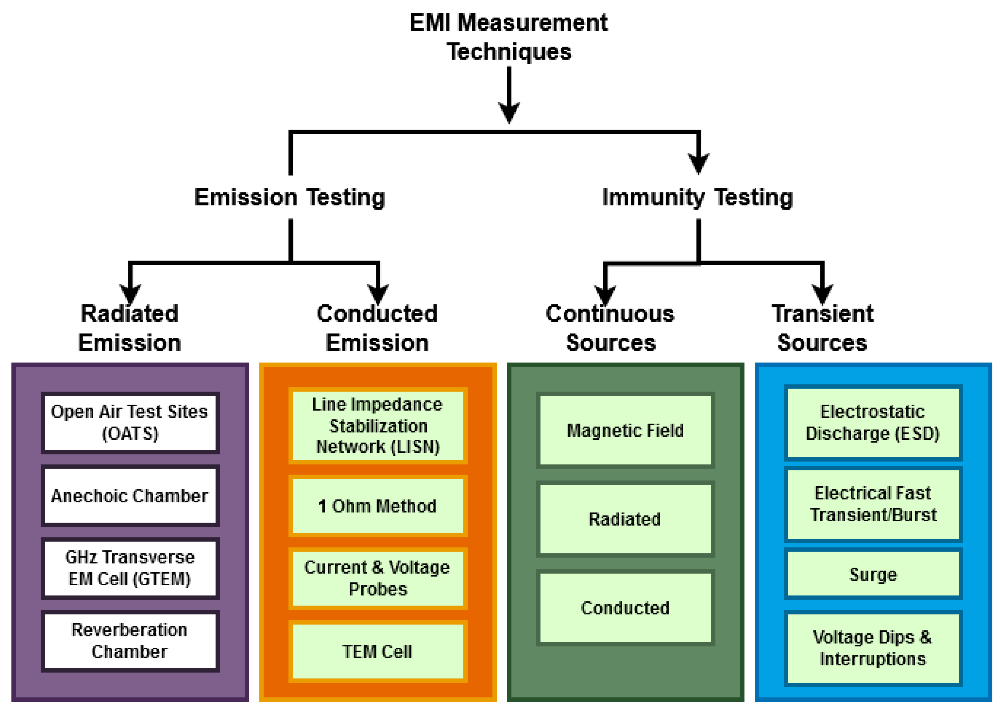
13] are more suitable and extensively used for EMI reduction, because they utilize the controlling parameters of the duty cycle and switching frequency for reducing the burden of noise. The different types of EMI measurement techniques are shown in
Figure 2.
Moreover, the IEEE standard 1459-2010 [
14,
15] defines the THD value and determines the quality of the consumed electrical energy. On the other hand, the IEEE 1459-2010 standard provides suitable descriptions to perform electrical measurement analyses under a wide range of power quality parameters, including sinusoidal, non-sinusoidal, stable, and imbalance conditions, which are prevalent in real-world situations.
In addition to that, the spreading of the output spectrum could also help to reduce the effects of EMI at different time instances. Here, the probability of switching patterns has been estimated for constructing the randomization model for reducing EMI in circuit designs. Similar to that, the spread spectrum frequency modulation is also one of the widely used methodologies for controlling the switching frequencies.
The overall harmonics level can be decreased by inserting the proper amount of harmonic voltage with the reference voltage. For this process, the optimal controlling techniques are utilized that intend to reduce the THD of the output voltage based on space vector pulse width modulation (SVPWM). Then, the switched capacitors also have the ability to suppress the EMIs by modifying the output spectrum. Yet, these methodologies are limited by the problems [
16,
17] of inefficient control, increased error values, and high noise content. In order to solve these problems, this research work intends to develop an intelligent random modulation technique for EMI reduction. In the methodology put forward, there is a combined approach to utilize maximum power electronic system performance with combined advanced control and modulation methods. First of all, randomization is presented through an FPGA-based design for random modulation purposes in order to reduce electromagnetic noise and spread the spectrum. On these grounds, an interleaved boost DC–DC converter topology is implemented for producing precision control pulses to be used to drive the switching devices. To further enhance harmonic performance, an innovative space vector-dithered sigma delta modulation (SV-DiSDM) scheme is proposed using a fully digitalized control method to reduce harmonic distortion and improve signal integrity. The efficiency and performance of the model proposed are extensively tested by using many evaluation parameters like total harmonic distortion (THD), switching frequency, switching loss, and distortion products, to ensure the stability and usability of the designed system. The major objectives behind this work are as follows:
the randomization concept is implemented with an FPGA design for random modulation;
the interleaved boost DC–DC converter topology has been utilized for generating the controlling pulses for actuating the switching devices based on the dithering model;
then, a space vector-dithered sigma delta modulation (SV-DiSDM) scheme is developed for reducing the effects of harmonics based on the digitalized controlling strategy;
the performance and efficiency of the proposed modeling are validated by using different evaluation metrics such as THD, switching frequency, switching loss, and distortion product.
The rest of the sections present in the paper are structured as follows: the existing controlling techniques used for the mitigation of EMI are discussed with their advantages and disadvantages in
Section 2. The detailed description of the proposed methodology is presented with its flow of illustration in
Section 3. The simulation results and performance analysis of both existing and proposed techniques used for reducing the EMI noise are discussed in
Section 4. Finally, the overall paper is summarized with its outcomes and future scope in
Section 5.
2. Related Works
This section discusses some of the existing works related to the concepts of electromagnetic interference (EMI) reduction with different types of DC–DC converter topologies. Also, it investigates the advantages and disadvantages of each work based on its operating steps and functionalities.
Loschi, et al. [
18] utilized a deterministic random modulation technique for reducing the EMI with the help of two identical DC–DC converter topologies. The main intention of this work was to analyze the comprehend behavior of low-frequency signals based on the knowledge of DetM and RanM. Moreover, the EMI highly depends on the interferences of the sources, testing components, and measurement models. Also, the short-term Fourier transform (STFT) technique was deployed along with the Hamming window for suppressing the switching noise contents. Rahman, et al. [
19] suggested a periodic dithering technique with an interleaved DC–DC converter topology for efficiently reducing the EMI. The key factor of using this technique was to maintain the switching frequency at a constant level with respect to the amplitude of the modulated signal. Moreover, different types of parameters, such as bandwidth, sweep, and contrast, have been estimated for generating the switching pulses. The advantages of this work were simple to design topology and a reduced current spectrum. Hizarci, et al. [
20] employed a T-type isolated bidirectional DC–DC converter topology for reducing the noisy contents with increased efficiency. Typically, the high-frequency switching activities could generate the EMI, which degrades the performance of the circuit with increased errors. Moreover, various techniques have been developed in the existing works for reducing the EMI, in which the random and modulated PWM techniques were more suitable for EMI reduction. In this work, the T-type switch has been modeled by considering the gain parameters of input voltage, output power level, reliability, and cost. Natarajan, et al. [
21] conducted a review on various methodologies used for reducing the EMI, which includes the following: Random modulation,
EMI filtering;
EMI shielding;
chaotic PWM controlling;
soft switching.
This work stated that the random modulation was one of the most suitable techniques used for suppressing the EMI, in which the switching frequency could vary with respect to the given random signal. In this model, the PWM technique was mainly utilized to generate the switching pulses according to the switching activities of DC–DC converter. Moreover, the other EMI reduction techniques are limited by the major problems of increased cost consumption, high complexity in design, and requiring some high-speed digital processors. Liu, et al. [
22] suggested a new EMI filtering technique for suppressing the EMI content, where the impedance analyzed was used to estimate the accurate impedance value of testing components. Jayaswal, et al. [
23] suggested a DC–DC buck converter topology for avoiding the switching losses and suppressing the EMI with ensured operating performance. The main purpose of this work was to increase the reliability and revamp the performance of the converter design.
Moonen, et al. [
24] demonstrated the ability of an accurate common mode choke (CMC) model in a 3D simulation environment. This enables in situ performance adjustments between minutes and hours as well as parametric assessments on parasitic behavior. Britto, et al. [
25] suggested the dual controller topology incorporated with an FPGA element for efficiently reducing the EMI. Here, the PWM generator has been utilized to control the signals and ensure smooth transitions.
Lezynski, et al. [
26] designed an efficient spectrum aggregation methodology for improving the performance of power converters with reduced EMI. The major factor of this work was to incorporate the benefits of the random modeling technique for providing opportunities to update the spectrum parameters during the analysis of data. Zhang, et al. [
27] developed an enhanced active modulation scheme with PWM for mitigating the EMI. The key benefit of this technique was that it does not require any accurate resolution at the time of measurement, and it efficiently reduced the harmonic contents based on linear mapping. Chen and Ma [
28] deployed a Markov continuous random spread spectrum modulation (RSSM) technique for efficiently suppressing the EMI with a stabilized duty ratio. The main purpose of this work was to obtain the nominal switching frequency with reduced harmonic contents. Here, it was mentioned that the SSM could be a more suitable technique for mitigating the EMI noise because it efficiently randomizes the switching frequency with the use of a random clock generator. Still, it is required to improve the overall performance with ensured regulated output and jitter.
Yang, et al. [
29] conducted a survey on various mitigation techniques used for reducing the EMI, which includes the external filters, internal filters, switching control mechanisms, and selection methodologies. The typical controlling techniques were mainly used to estimate the level of EMI for boosting the output power level of converters. Based on this work, it was analyzed that the modeling parameter need to be highly concentrated for suppressing the EMI noises. Pareschi, et al. [
30] presented a clear analysis on PWM techniques and resonant converter classes for ensuring improved system performance. Normally, the spread spectrum was one of the extensively used mechanisms for reducing the EMI in many circuitry applications. Nassireddine, et al. [
4] utilized a frequency domain approach for accurately predicting the EMI in DC–DC converters. Here, the Laplacian transformation was also utilized to improve the efficiency of the suggested scheme with the help of buck converter topology.
Early focus of work was typically aimed at passive filtering techniques, such as the application of LC filters, ferrite beads, and shield material. They are older, less complex technologies with relative installation simplicity, but the possible disadvantage is greater size, weight, and inflexibility of application over a wide number of frequency bands. For instance, FPGA-based and DSP-based digital controllers are used to achieve a real-time pulse modulation scheme and pattern modulation switching for limiting EMI. Bringing in the literature, in the process, it is realized that despite still being the foremost ones, traditional methods especially continue to remain essential in high-power applications, conventional methods now complemented or replaced by even smarter and more advanced systems capable of dealing with electronics’ miniaturization and increasing complexity in recent times.
The second key area of comparison is in modulation schemes employed to limit EMI. Conventional fixed-frequency PWM techniques, though extremely prevalent due to simplicity and determinism, have been found to generate harmonics that are clumped with the impact of generating narrow spectral peaks, elevating systems to EMI concerns. Spread spectrum and dithering-based modulation techniques have been confirmed by literature to have the capability of spreading energy across a larger frequency band and, as a result, controlling peak level emissions. Sigma–delta modulation (SDM), random pulse position modulation (RPPM), and space vector pulse width modulation (SVPWM) by dithering techniques have proven to have drastic EMI mitigation across very critical frequencies. SVPWM with dithering, however, offers high control precision along with effective spectral distribution and hence forms the best solution to EMI-aware designs. Combining the findings above, it is ensured that optimal EMI reduction is typically achieved through the use of a combination of frequency-domain spectral flatness and time-domain signal processing by means of holistic design strategies.
From this review, it is found that the existing techniques are mainly focusing on reducing the EMI noises in the circuit design by using different types of filtering, component selection, and switching control mechanisms. Still, it is limited by the following problems:
restricted by the voltage conversion range;
increased conduction losses;
increased stress in both current and voltage;
reduced efficiency;
high noise content.
Typically, the EMI is defined as the electromagnetic energy, which highly affects the performance of electrical components with an undesirable responses and operational failures. Typically, the EMI can be suppressed based on the operations of grounding, shielding, and filtering. Hence, the proposed work objects to develop a new randomization based modulation scheme for improving the overall performance of system with reduced EMI.
3. Materials and Methods
This section presents a detailed description about the proposed randomization controlling methodology used for mitigating the EMI noise. The main contribution of this work is to implement efficient control and converter topologies based on the randomization model for minimizing the EMI. Here, the interleaved boost DC–DC converter is utilized to regulate the voltage output by properly operating the switching components. Because the random and unregulated power supply may increase the level of harmonics on the load side, this work sets out to properly regulate the output based on the controlling signals generated by the controller. In this system, a randomization based space vector-dithered sigma delta modulation (SV-DiSDM) scheme is developed for generating the pulses to operate the switching components of converter, which helps to effectively reduce the level of THD and loss of power. Moreover, the two-level inverter design is utilized in this system to suppress the harmonic contents, where the switching scheme is simplified based on the mapping of the voltage reference vector with the space vector plane. In addition to that, the random dither generation unit is utilized in the controlling model, which comprises the sign discriminator and random magnitude adjustment portions. In this model, the random value between the range of (0, 1) is selected at every sampling instance, based on this value, the sign discriminator can decide whether the dither is implemented or not. If the signs of both input and output differ from each other during the sampling instance, the dither must not be used, because it avoids the excessive reduction of switching frequency. The overall schematic illustration of the proposed system is shown in
Figure 3a.
The originality of the work done lies in the combination of a randomized control approach with a high-performance modulation method, i.e., the space vector-dithered sigma delta modulation (SV-DiSDM), specially designed to minimize electromagnetic interference (EMI) in power electronic circuits. This paper illustrates an active smart control mechanism in which important switch parameters like the duty cycle, switching frequency, and signal modulation are rendered random within bounded limits in order to efficiently dissipate the harmonic energy over a wider range of frequencies. This randomization process, in addition to aiding the flattening of the emission spectrum, thus reducing interference, is also utilized to minimize peak harmonic content that normally contributes to EMI problems. The interleaved boost DC–DC converter topology is also used to increase this effect by distributing the ripple current among multiple phases, which works in conjunction with the modulation scheme and results in increased EMI suppression without any degradation in power conversion efficiency.
The most significant contribution of this work is the development and application of the SV-DiSDM approach, where space vector modulation is used creatively in conjunction with a dithering-improved sigma–delta architecture. Both architectures are utilized by combining the strengths of accurate voltage regulation and noise-shaping ability to achieve a better control system with less harmonic distortion whenever it operates under dynamic load conditions. Moreover, the FPGA hardware-based digital realization of the control model is reconfigurable and high-speed processing enabled, and, therefore, the suggested solution is highly flexible for real-time power electronic applications. The comparative study carried out in terms of performance factors like total harmonic distortion (THD), switching frequency deviation, switching loss, and distortion product further assures the superiority of the suggested method compared to conventional approaches. Through addressing the inherent drawback of complexity, inefficiency, and harmonic distortion of current EMI mitigation approaches, this work formulates a new and realistic paradigm for next-generation EMI-resistant power electronic converters.
3.1. FPGA Design with Randomization
The FPGA element contains many IO devices, ADCs, DACs, and IO lines that are accessed through the bus interface. During this design, it is very essential to ensure the processes of trimming, IO measurements, and triggering with the available functions. In the proposed design, the arithmetic complexity of the fuzzy logic genetic architecture (FLGA) was reduced with the simple logical operations, and also the controlling techniques required the IO resources for processing. Here, the PWM modulation scheme was mainly used to control the switching activities of the converter with respect to the parameters of duty cycle, switching frequency, and signal. Then, the duration of high states were determined below:
where
indicates the clock tick for the period,
represents the onboard frequency,
denotes the switching frequency, and
is the single-cycle loop. This modulator can operate dynamically with the factor of PWM signal S, and its value can be randomly changed. Moreover, the random number generation is performed in this work to suppress both the switching frequency and harmonics. Normally, the random generator is highly complicated for random controlling techniques, hence, is it essential to utilize the fixed-point pseudo-random function architecture (FPFA) feature with the fixed point operation. Then, the stream pseudo-random number is created as follows:
where
indicates the random number provided by the LCG modulator,
and e are the coefficients of the linear congruential generator (LCG). During the implementation process, the random probability density function has been computed to improve the process of randomization. Here, the random stream is utilized to change the random values according to the period of PWM, which is estimated based on the duty cycle of the random modulation scheme, as shown below:
Where, defines the final updated value of the random number, D is the duty cycle, and indicates the index value.
3.2. Interleaved Boost DC–DC Converter
The Schematic representation of the interleaved boost DC–DC converter is shown in
Figure 3b. Due to its increased efficiency with reduced voltage/current ripples, an interleaved boost DC–DC converter topology is most suited for EMI suppression, which also reduces the size of both the inductor and the capacitor. In this design, the three-phase interleaved boost DC–DC converter [
31] topology has been utilized to generate the control signals for the switching activities. The EMI attenuation in the converter is done through the application of a periodic dithering technique, where the controlled oscillation of the switching duty cycle or switching frequency is utilized to spread the spectral energy. This decreases peak electromagnetic emissions by spreading harmonics across a broader frequency band, hence minimizing interference. On the converter side, the smaller output ripple current requires a smaller capacitor at the load side. But, the common EMI is generated according to the high voltage at the components of switches and diodes in the converter. During this process, the switching frequency is maintained with a constant value by dithering the frequency of the PWM signal. Due to the increased number of switches and phase-shifting operations, the converter could be noisy under a fixed switching frequency. To satisfy the EMI standard, a dithering-based filtering technique is employed in this model to minimize the significant amount of space. When compared to other costly filtering techniques, the frequency dithering model is used to reduce the EMI at reduced cost. Moreover, the dithering parameters considered in this design are the bandwidth of the switching frequency, phase of dithering signal, and sweep.
Then, the converter’s frequency variation is assessed based on the amplitude of the modulating signal. The key parameters used for designing this converter topology are as follows [
32]: bandwidth, contrast, and sweep, in which the bandwidth is determined based on the frequency range of the dithered signal.
As depicted in
Figure 3a, the PWM function
can be generated with respect to the duty cycle
and switching period
by using the following equation:
where
indicates the magnitude of the nth harmonic and
represents the phase of the nth harmonic. Based on dithering, the switching frequency of the PWM signal has been modulated, and its nth is estimated as follows:
where
represents the frequency of the dithering signal,
and
are the maximum and minimum values of the signal, respectively. Consequently, the modulation index
has been computed as shown below:
where the sweep is defined as the frequency of dithering; if it increases, the value of the modulation index can be decreased. Similarly, the contrast has been estimated based on the phase shift between the dithering signals.
As shown in
Figure 3b, the periodic pulse signal is generated as follows:
Then, the interleaved boost DC–DC converter is phase shifted with respect to the kth phase for obtaining the periodic pulses as shown below:
where
defines the maximum value of the PWM signal, N indicates the switching frequency, D is the dithering period, Di denotes the ith switching period, n represents the number of phases, and
is the pulse duration. Subsequently, the amplitude of the dithering signal, shown in
Figure 4, can be represented as follows:
where
indicates the frequency of the signal and
, and D represents the dithering period.
3.3. DiSDM with Random Dither Generation Unit
The main contribution of this work is to develop a space vector-dithered sigma delta modulation (SV-DiSDM) scheme for reducing the effects of harmonics based on the digitalized controlling strategy. It is a kind of pulse density modulation scheme [
33] and is mainly used for controlling the switching activities that result in the increased harmonic content. The block representation of the proposed SV-DiSDM ADC design for EMI reduction is shown in
Figure 5, where the
coordinate system was utilized to represent the space vector model. Here, the mapping of the reference space vector is performed with two DiSDMs, in which one is used for the resolved vector space
at
. Then, the error value
is obtained by estimating the difference between the quantizer vector output
and reference vector
. Consequently, the vector quantization methodology has been utilized to quantize the error value for attaining the switching vector of the inverter
. The dithered signals, such as
and
are appended with the space vector, and these signals can be controlled by both the input of the space vector and output vector. Moreover, the feedback signals
and
are obtained with the switching signals of
,
and
by using the quantized vector, and these signals are converted into
for creating the error signals of
and
. The block representation of the random dither generation unit is presented in
Figure 6 and
Figure 7.
The random dither generation unit [
34] comprises two stages such as the magnitude adjustment and signal discrimination, where the random number is selected with the sequence of 0 and 1 at each time instant. Consequently, its bias has been diminished with the value of 0.5 in the magnitude adjustment unit. Then, the main functionality of the sign discriminator is to determine whether the dither can be utilized or not. If the sign of both the input and output of DiSDM are not equal during the sampling instant, it cannot be used, which helps to suppress the loss of switching frequency. Typically, the error value obtained from the DiSDM is a random value, which can be mapped into the vector plane by using the vector quantization model. Here, the switching vectors are determined based on the amplitude of the reference space vector. Due to the random operations of SVPWM, it reduces the complex arithmetic operations and computations. The key benefits of using this scheme are reduced cost, low memory space, and increased speed.
4. Results and Discussion
This section presents the results and discussion of both existing and proposed schemes by using various evaluation metrics. The simulation model setup for the performance evaluation of the developed EMI minimization technique was built upon a full-fledged MATLAB/Simulink environment. The model included an interleaved boost DC–DC converter topology, built from fundamental power electronic devices like inductors, switches, diodes, and output filters. The control method was realized through a digital control block including the space vector-dithered sigma delta modulation (SV-DiSDM) scheme. A periodic dithering function was implemented to dynamically alter the switching parameters, thereby accurately simulating the randomization behavior. A pseudo-random number generator based on the linear congruential generator (LCG) was also utilized for signal modulation, and control pulses for switching were generated accordingly. For efficiency analysis of EMI suppression, total harmonic distortion (THD), switching frequency, and electromagnetic spectral distribution were tracked by respective measurement blocks. This overall setup provided a correct performance evaluation of the proposed technique for different operating conditions. In the proposed work, the periodic dithering model was utilized for designing the interleaved boost DC–DC converter topology, where the pulses were used to controlling the switching activities.
Figure 8a,b compares the PWM spectrum of both fixed and dithering techniques, respectively, under varying frequencies in terms of KHz. Based on this evaluation, it was observed that the dithered PWM could efficiently reduce the peak of the spectrum, which helped to suppress the harmonic contents.
Figure 8a,b shows the generated dithered PWM signal for the bandwidth of 16 kHZ to 24 kHz with the sweep of 1000 Hz and 500 Hz, respectively. By using these results, the sweep effect was analyzed with respect to varying frequency in terms of KHz. From the evaluations, it was observed that the peak value of the spectrum was efficiently reduced with the sweep value.
Figure 9 shows the analysis of EMI emission peak level with respect to varying modulation index, where
indicates the frequency deviation, and m is the modulation index. In this analysis, the EMI measurement is validated based on the optimum value of the modulation index in the plot. According to the evaluation, it was analyzed that the highest EMI reduction was achieved with the varying modulation index.
Figure 10 depicts the output ripple voltage of the interleaved boost DC–DC converter with respect to varying modulation index values. Similarly, the efficiency of the converter was estimated for varying frequency deviations and modulation index values, as shown in
Figure 11. Typically, the efficiency of the converter highly depends on the switching pulses generated by the controller. Moreover, the voltage deviation was also estimated with respect to different modulation index values, as shown in
Figure 12. From the obtained results, it was analyzed that the proposed new randomization-based modulation scheme provided improved performance results by efficiently reducing the level of EMI.
Figure 13 analyzes the total harmonics distortion (THD) level of both existing and proposed schemes with respect to varying modulation index, which includes sigma delta modulation (SDM) [
35], space vector pulse width modulation (SVPWM) [
33], random PWM [
34], and space vector SDM [
35]. From the evaluation, it was identified that the proposed DiSDM technique efficiently reduced the level of THD for all modulation indexes when compared to the other techniques.
Similarly, the normalized switching frequency level of both existing and proposed modulation schemes was validated with respect to varying modulation index, as shown in
Figure 14. This analysis showed that the SVPWM and PWM techniques had a constant normalized switching frequency. When compared to the other models, the proposed technique provided an improved switching frequency by efficiently controlling the switching pulses.
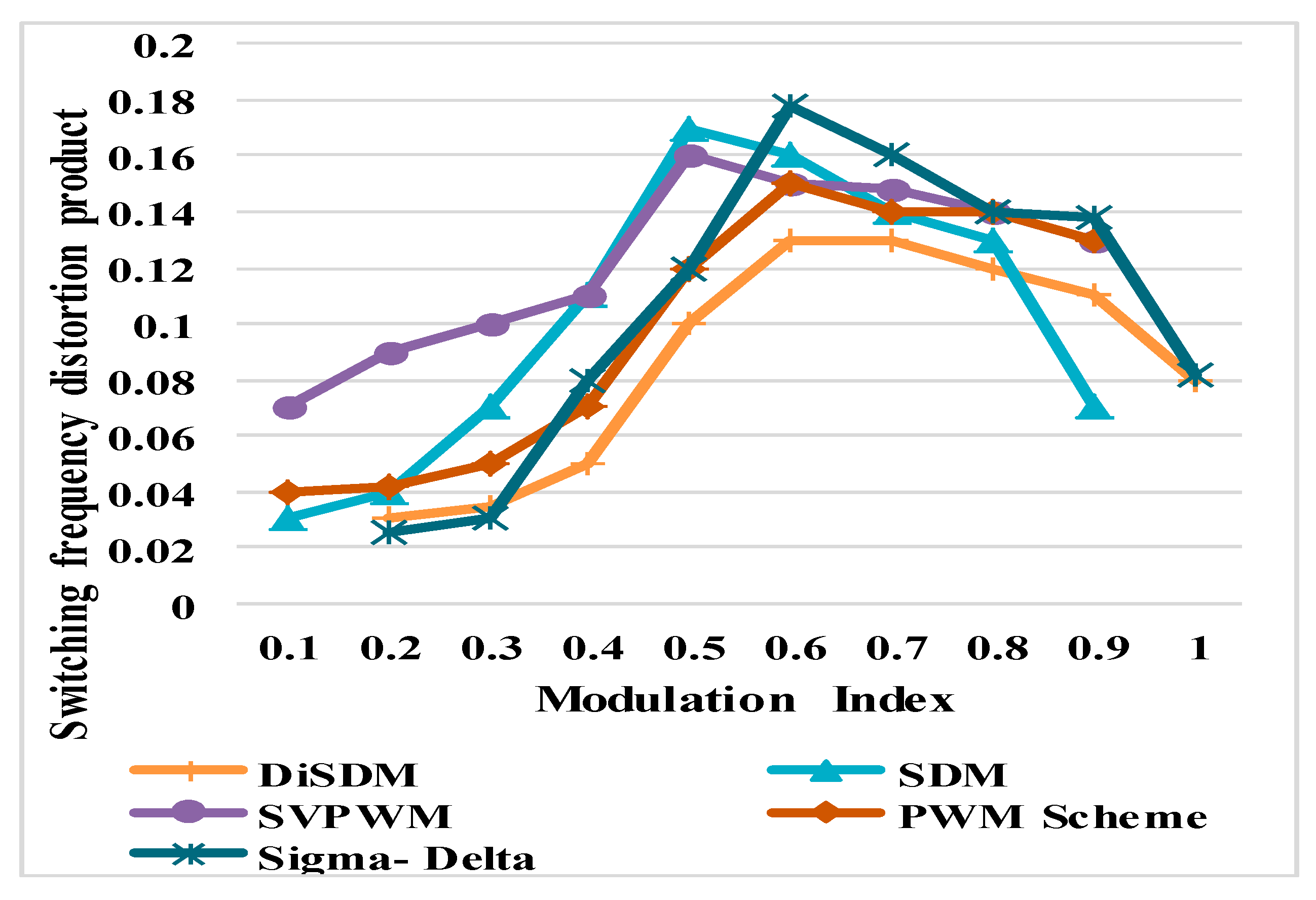
Figure 15 compares the existing and proposed techniques based on the measure of switching frequency distortion product with respect to varying modulating index. The obtained results show that the distortion production of the proposed DiSDM technique was efficiently reduced at all modulation indexes when compared to the other techniques. It proves the overall effectiveness and efficiency of the proposed mechanism with reduced error values and harmonics. Consequently,
Figure 16 shows the switching loss of both existing and proposed techniques under varying modulation indexes. Typically, the controlling mechanism has the key responsibility for reducing both the switching and conduction losses by efficiently triggering the pulses for actuating the switching devices. Hence, the loss factor highly depends on the operating functions and characteristics of the generated pulses. From the analysis, it was evident that the switching loss of the proposed DiSDM technique was effectively reduced when compared to the other modeling schemes. Because the dithering model was utilized for suppressing the noise contents in the proposed mechanism, this helped to prevent the switching losses.
Figure 17 and
Table 1 compare the harmonic spread factor of both existing and proposed controlling models with respect to the voltage and current measures. Typically, the harmonic spread factor is mainly used for determining the quality of signals, which is estimated as follows:
where
represents the harmonic spread factor,
is the statistical expectation value,
is the total number of harmonics,
denotes the magnitude of harmonics, and
is the average value of harmonics. From the evaluation, it was identified that the proposed DiSDM scheme provided a reduced harmonics spread factor in both voltage and current, when compared to the other models.


