
A Fast Surrogate Model-Based Algorithm Using Multilayer Perceptron Neural Networks for Microwave Circuit Design

 ,
,  ,
,  ,
,  , and
, and 
Abstract
1. Introduction
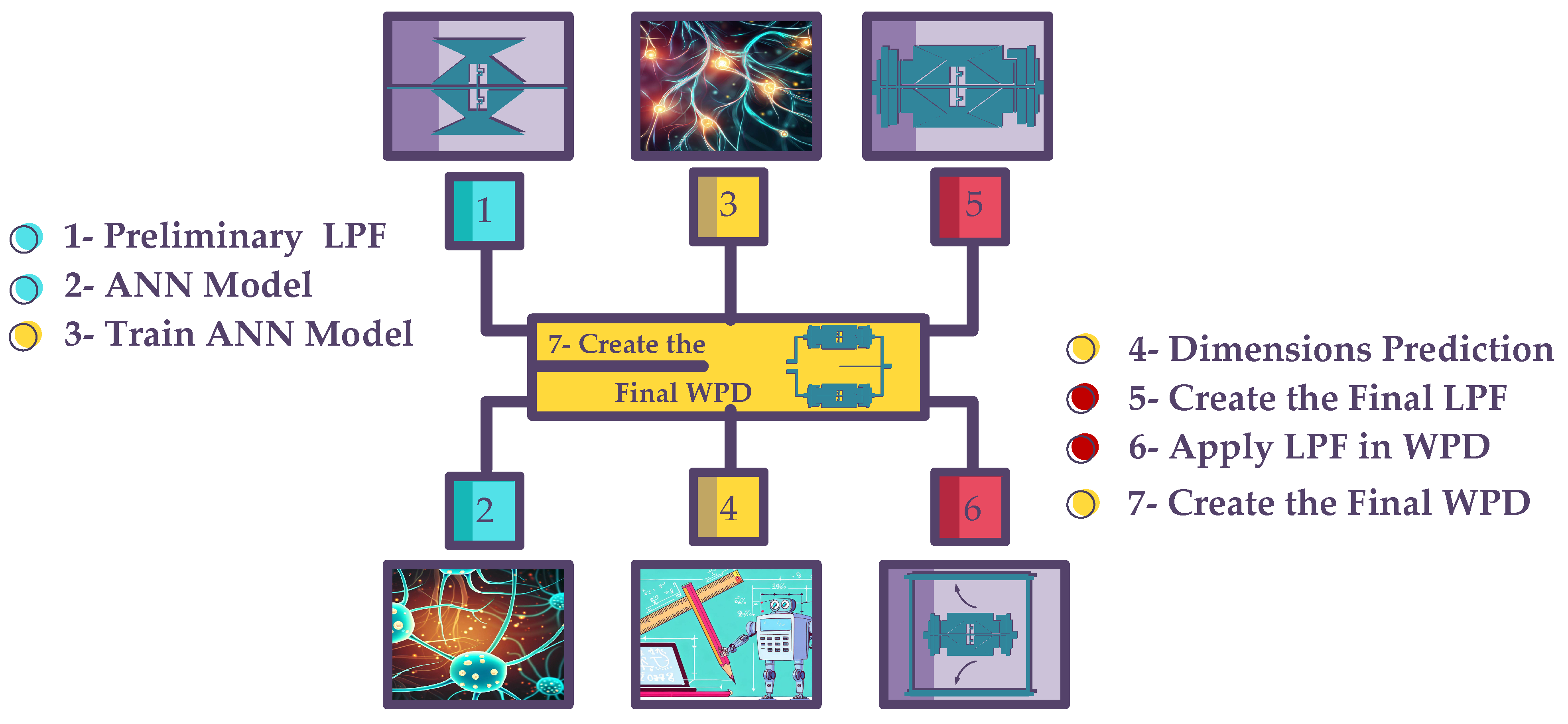
2. Design Algorithm
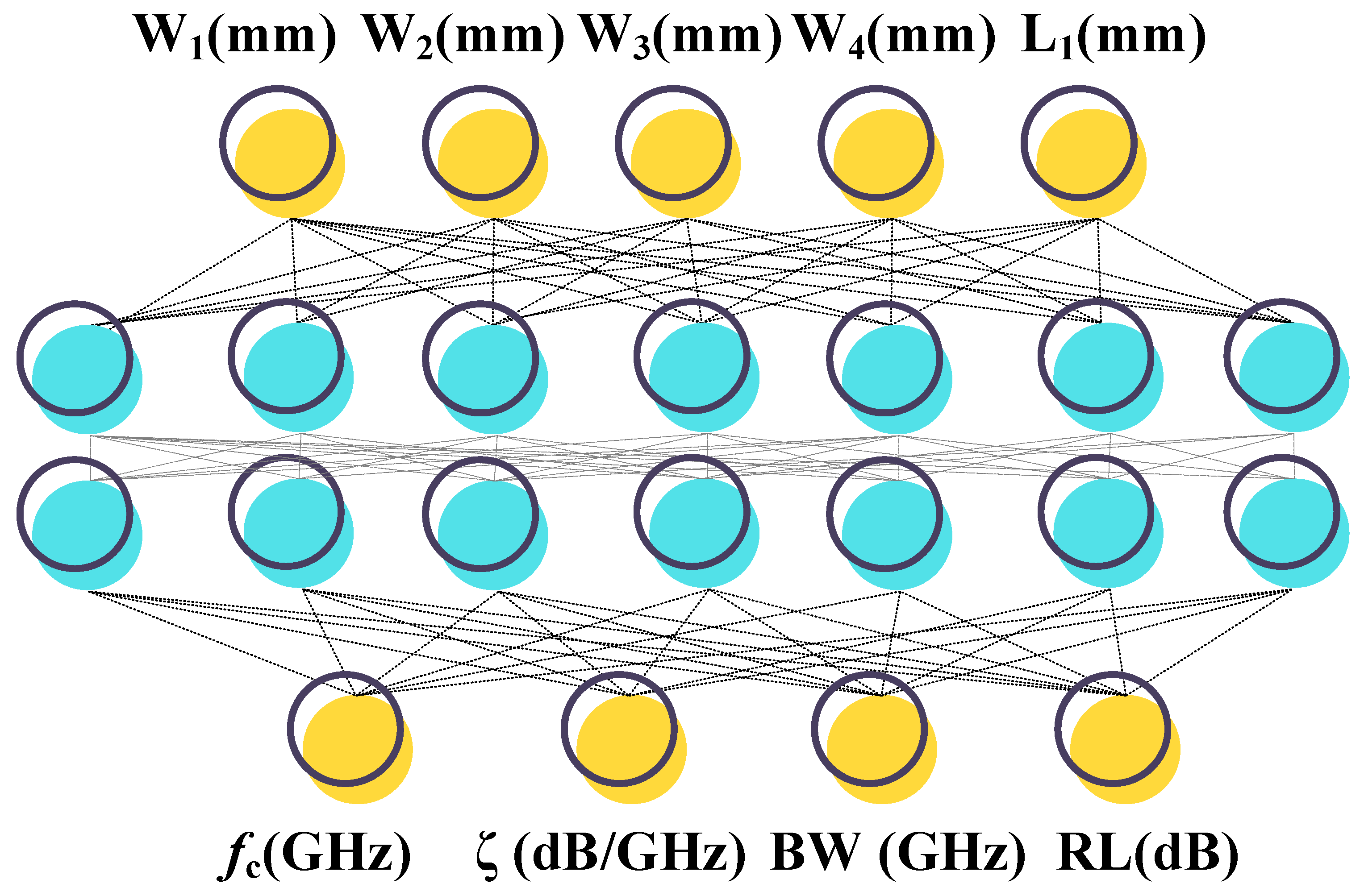
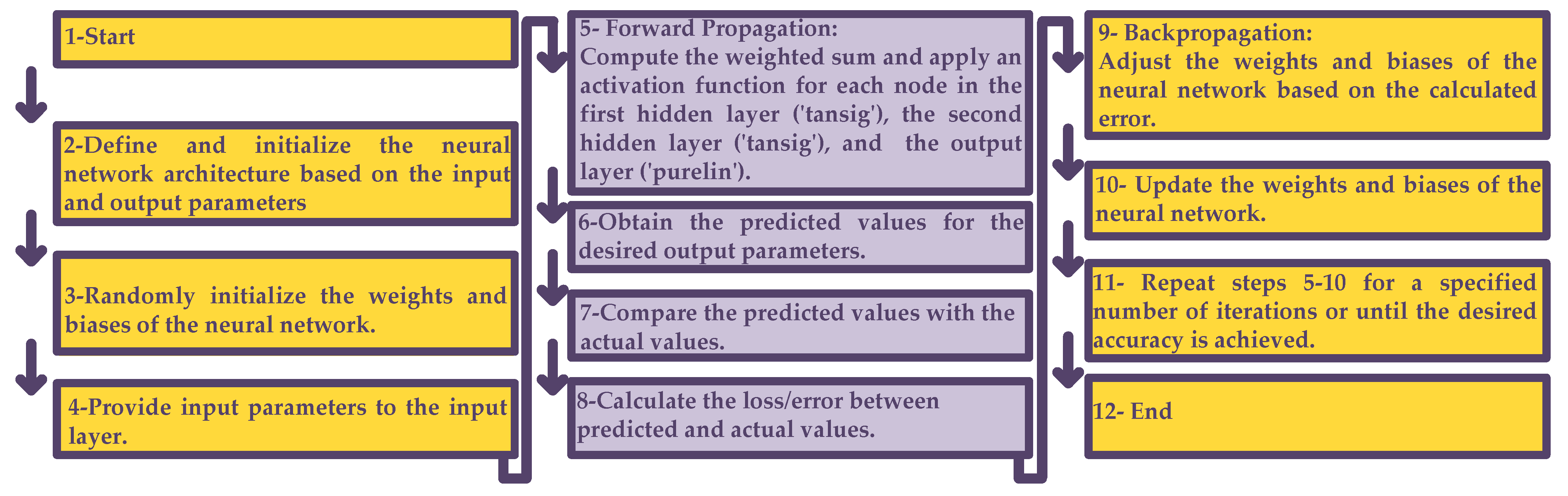
2.1. The Architecture of the Proposed ANN Model
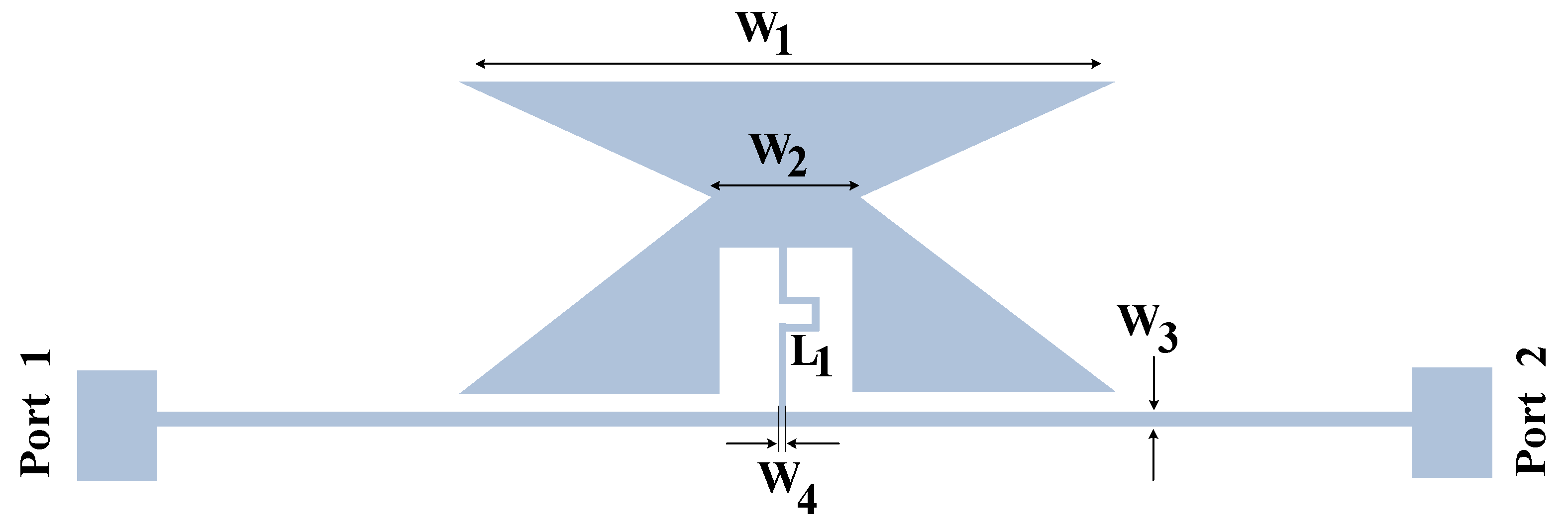
2.2. Proposed Resonator Design
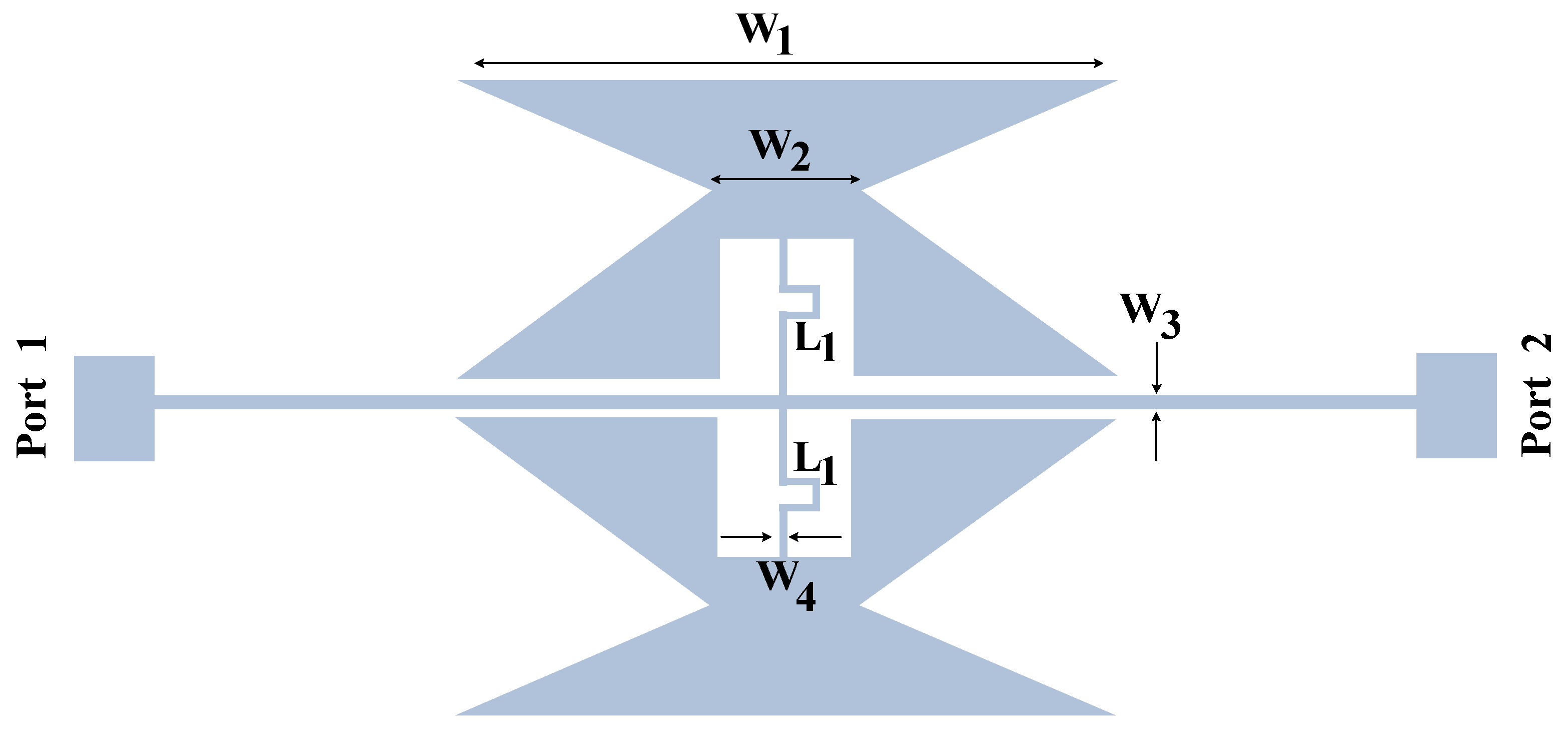
2.3. Proposed Basic Single Polygonal Resonator Design
2.4. Proposed Preliminary Dual Polygonal Resonator Design
2.5. Applying The Proposed ANN Model
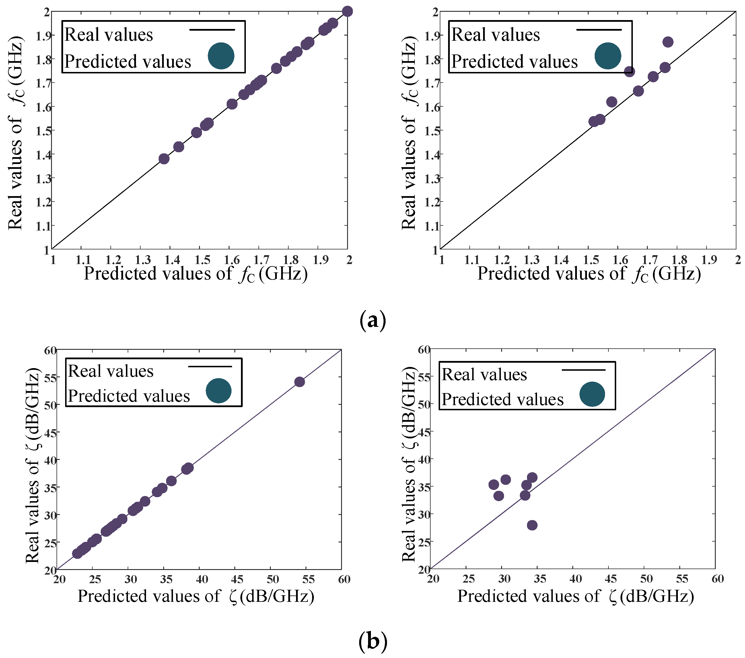
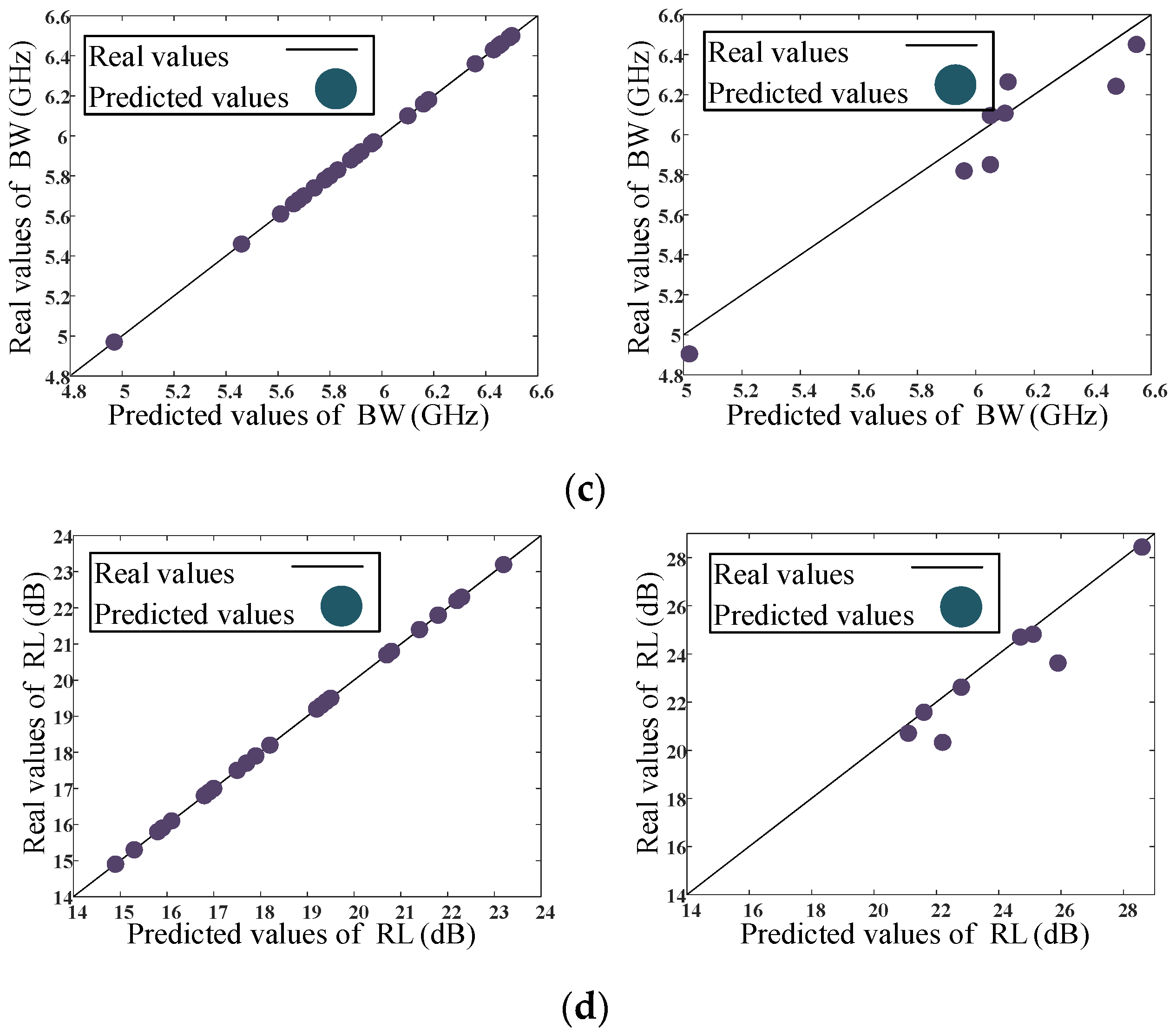
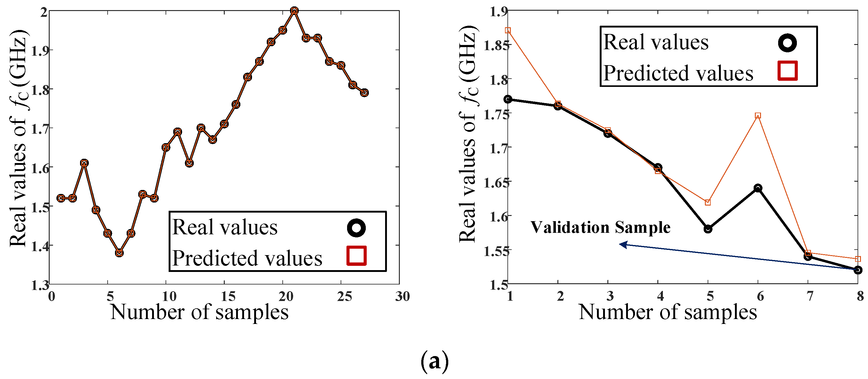
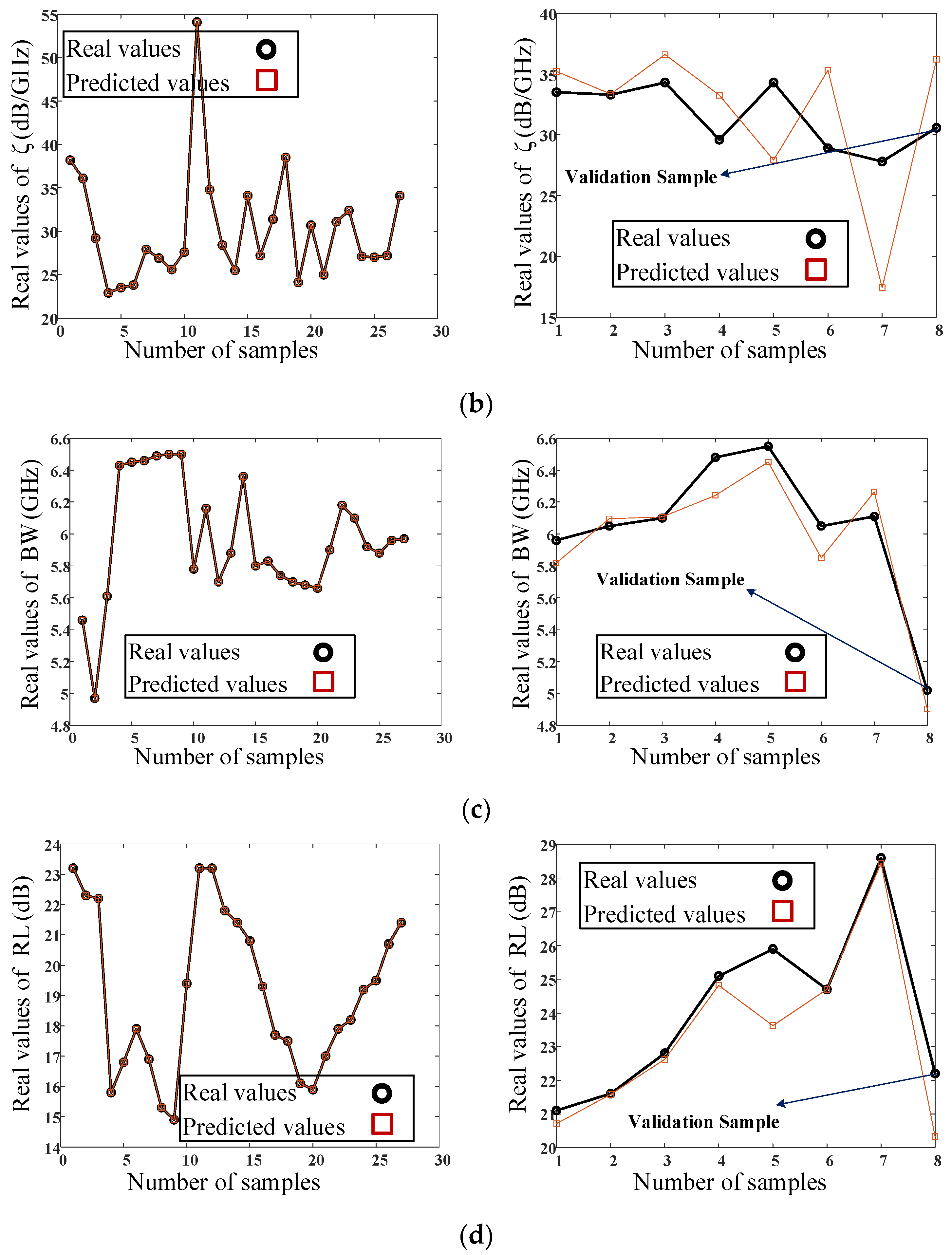
3. The Results of the Proposed ANN Model
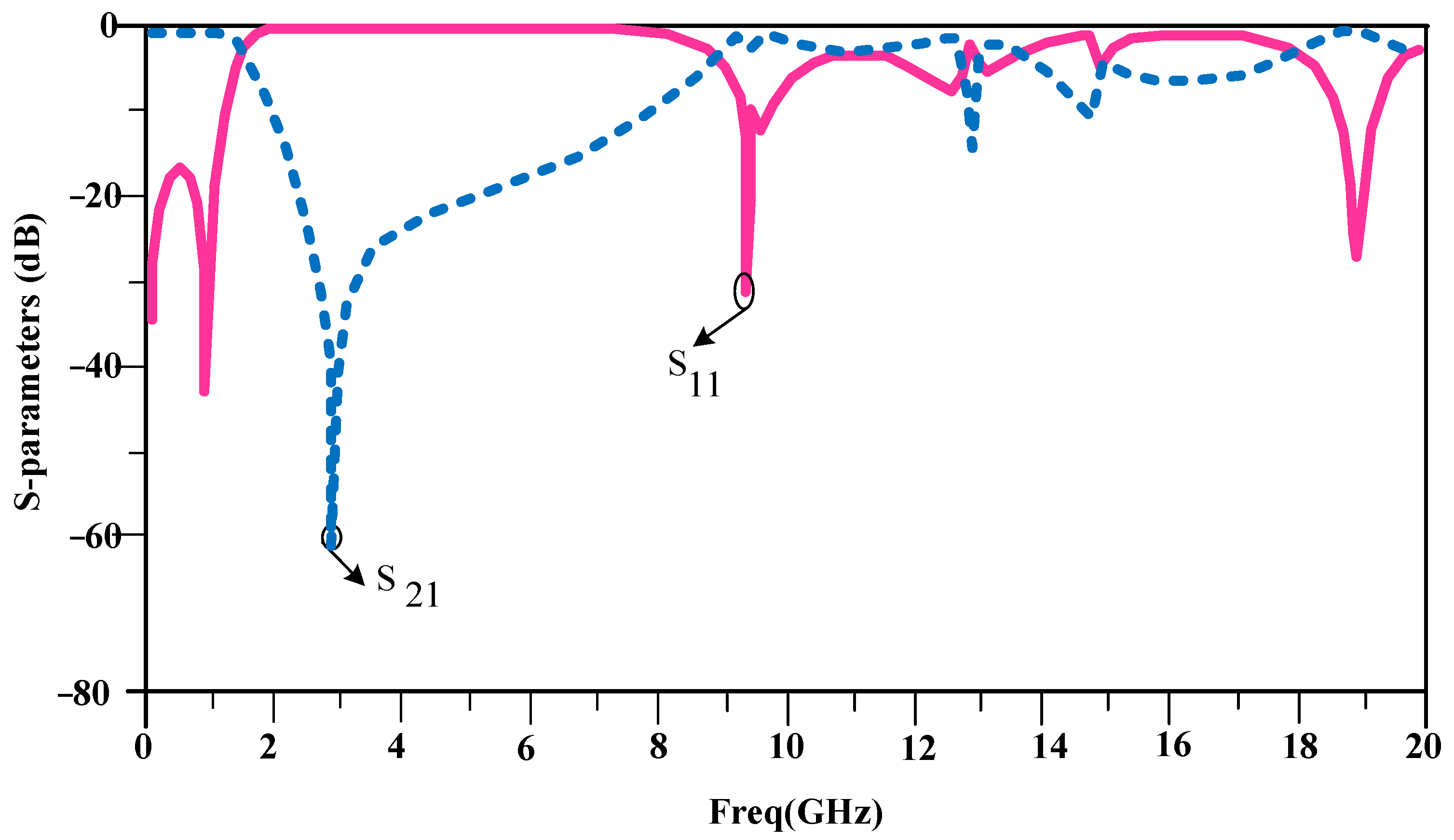
4. The Design of the Proposed Filter
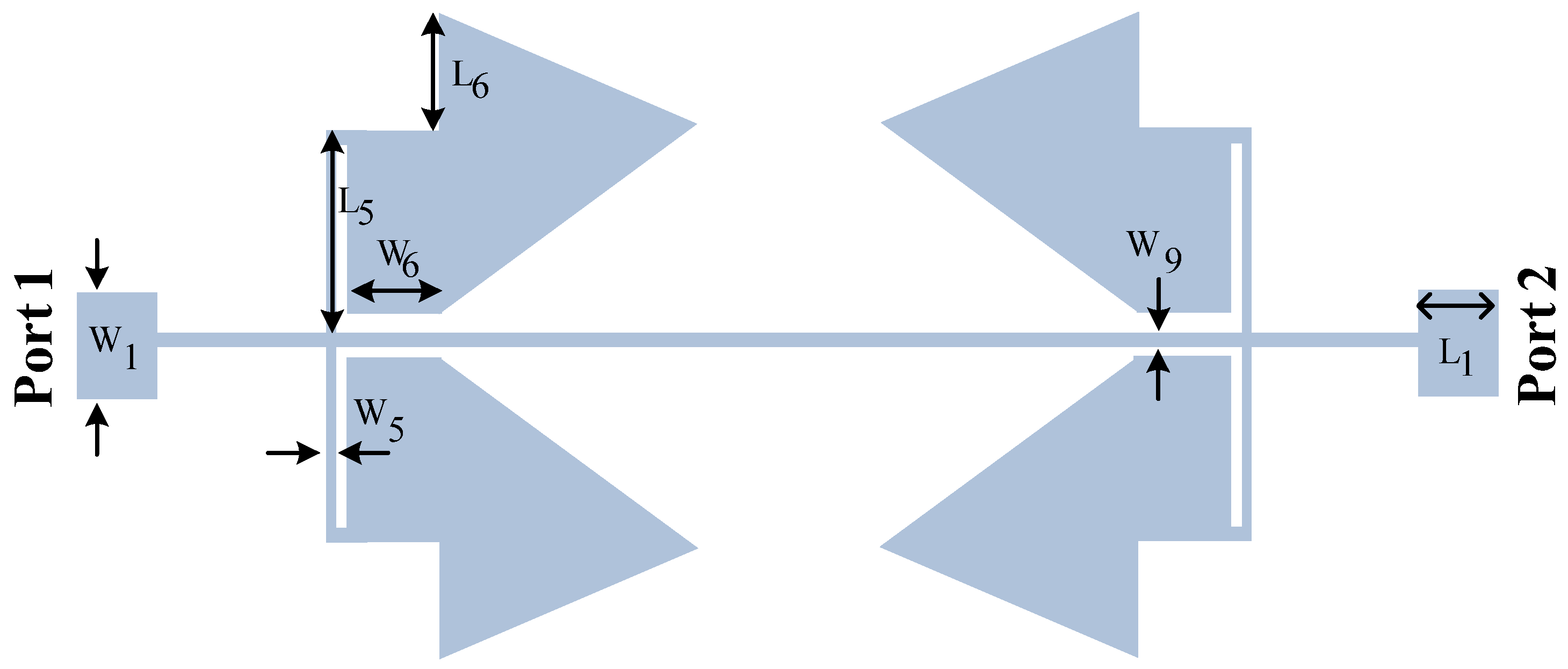
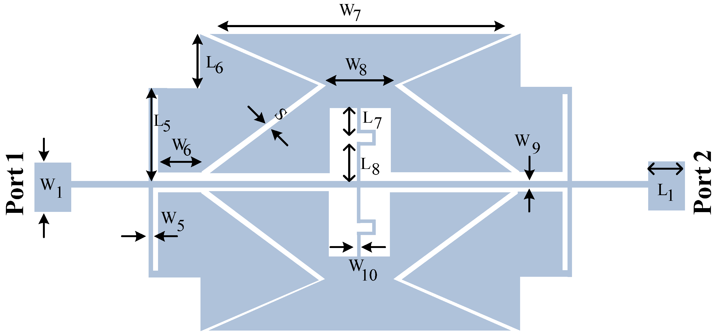
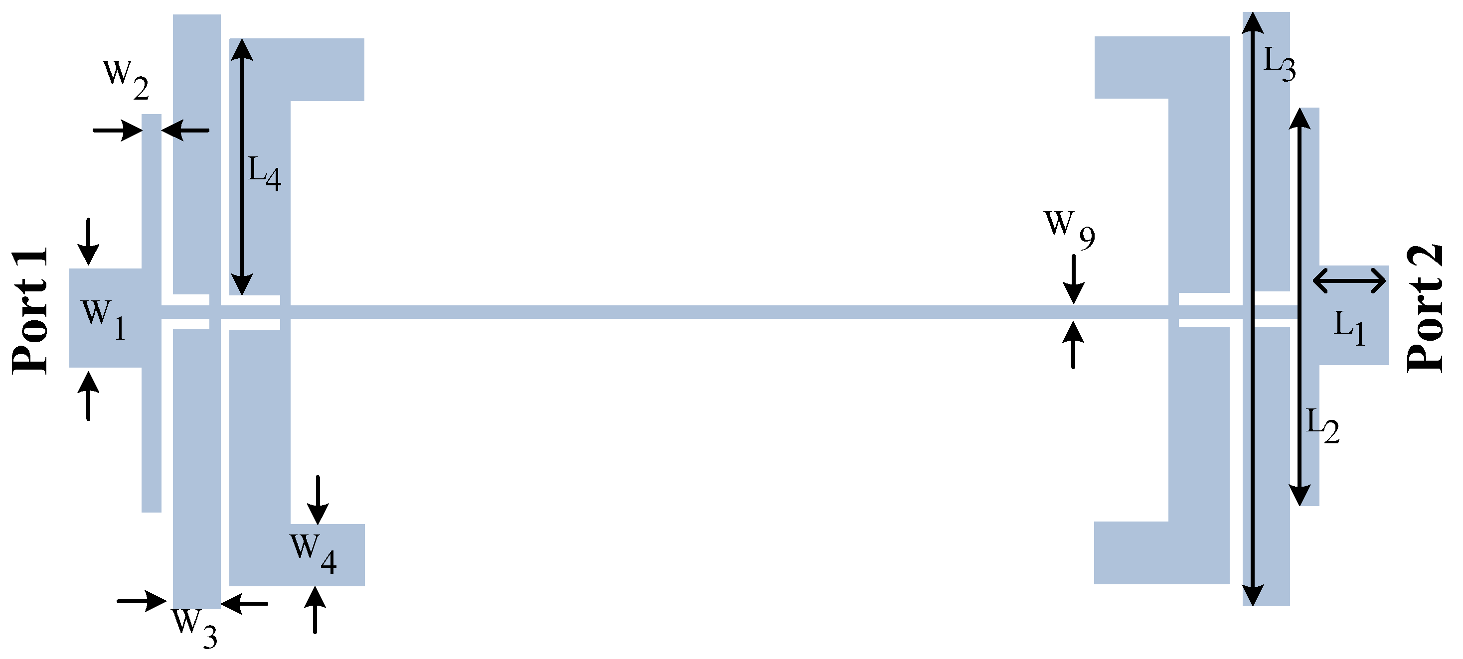
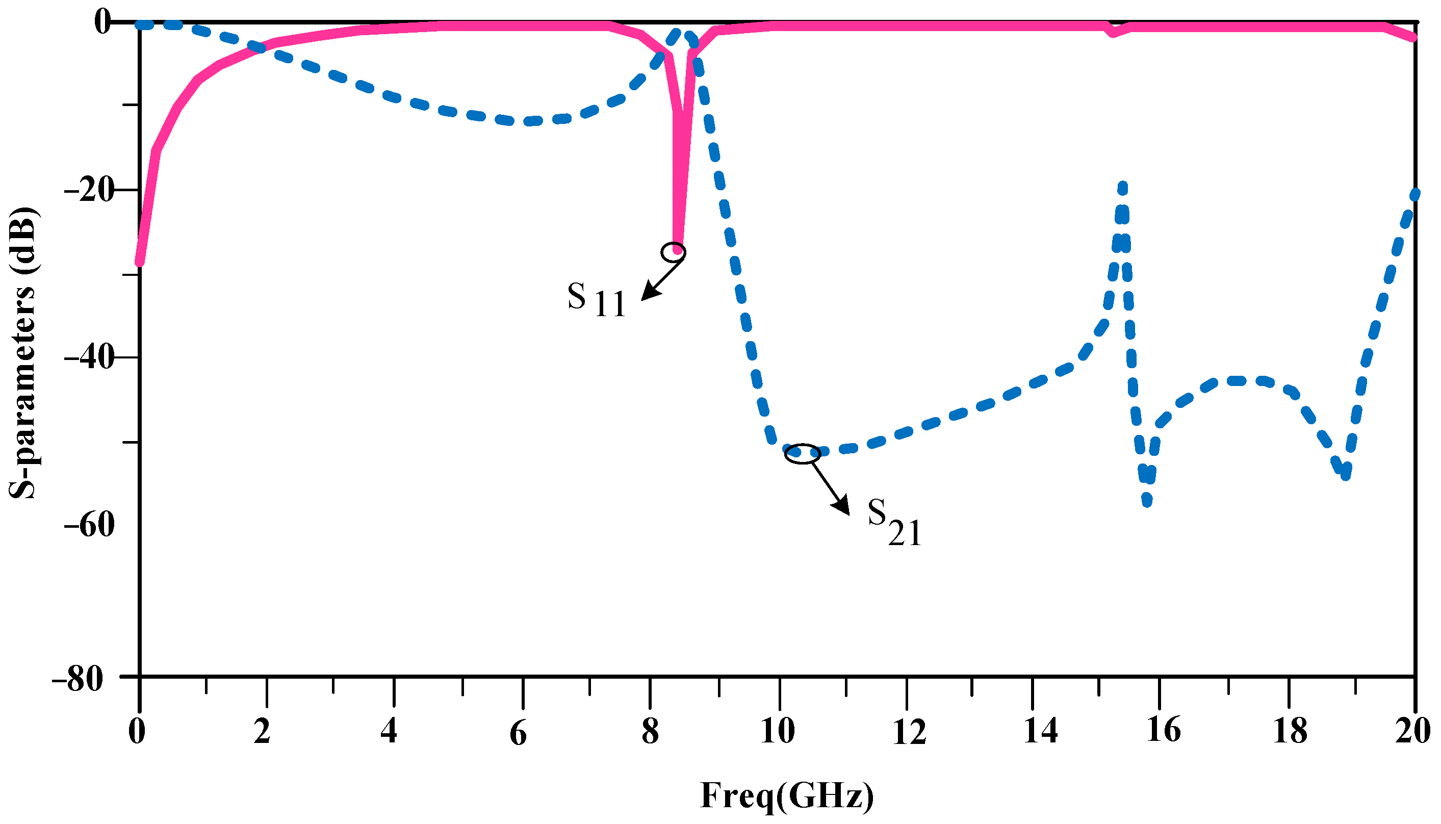
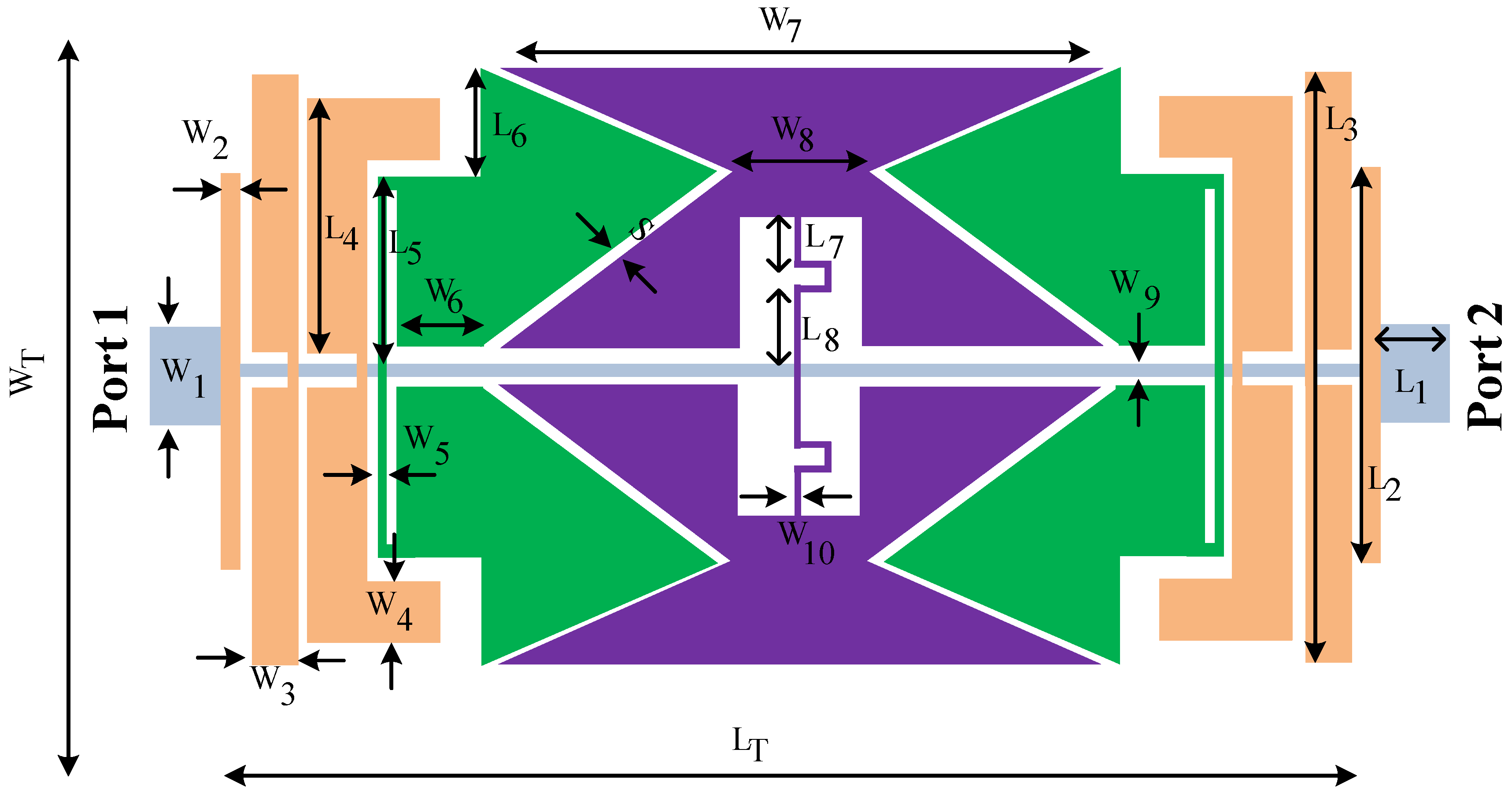
4.1. The Design of the Proposed Dual Side Resonators
4.2. Proposed Combined Resonator Design
4.3. Proposed Suppressor Cell Design
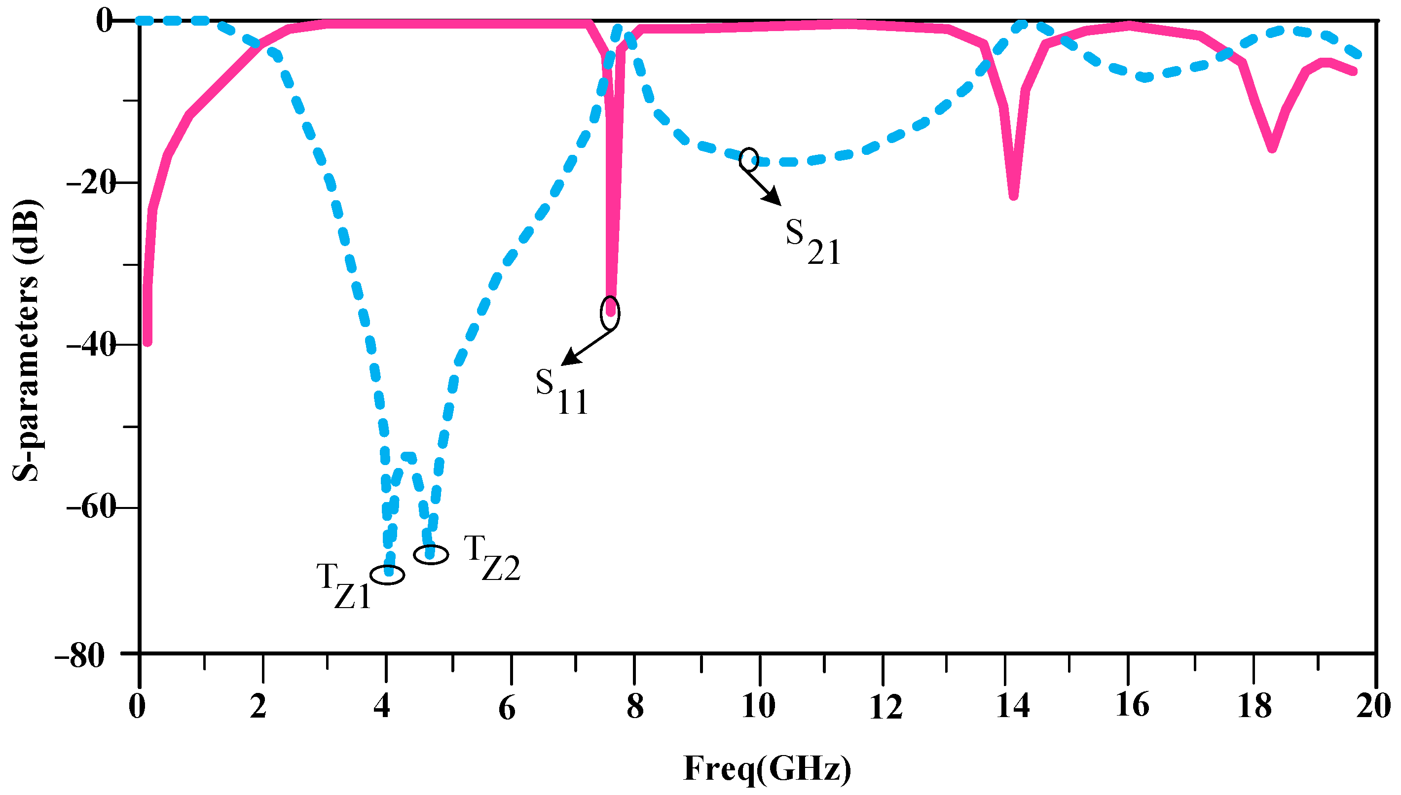
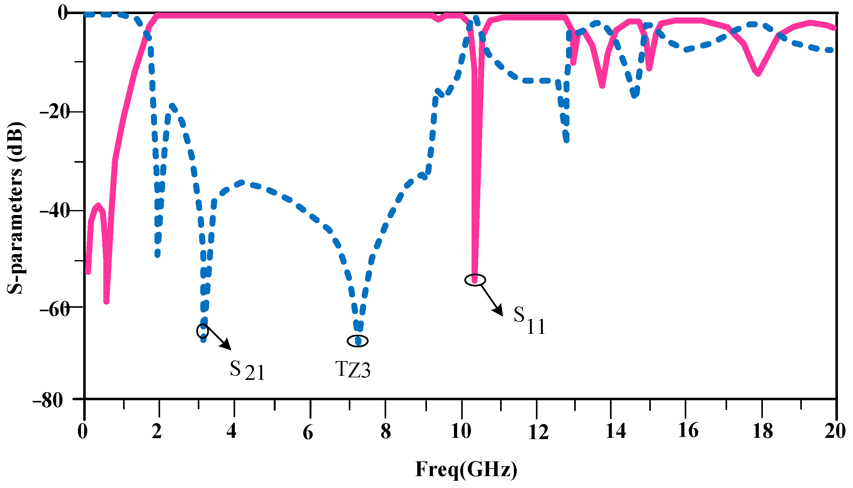
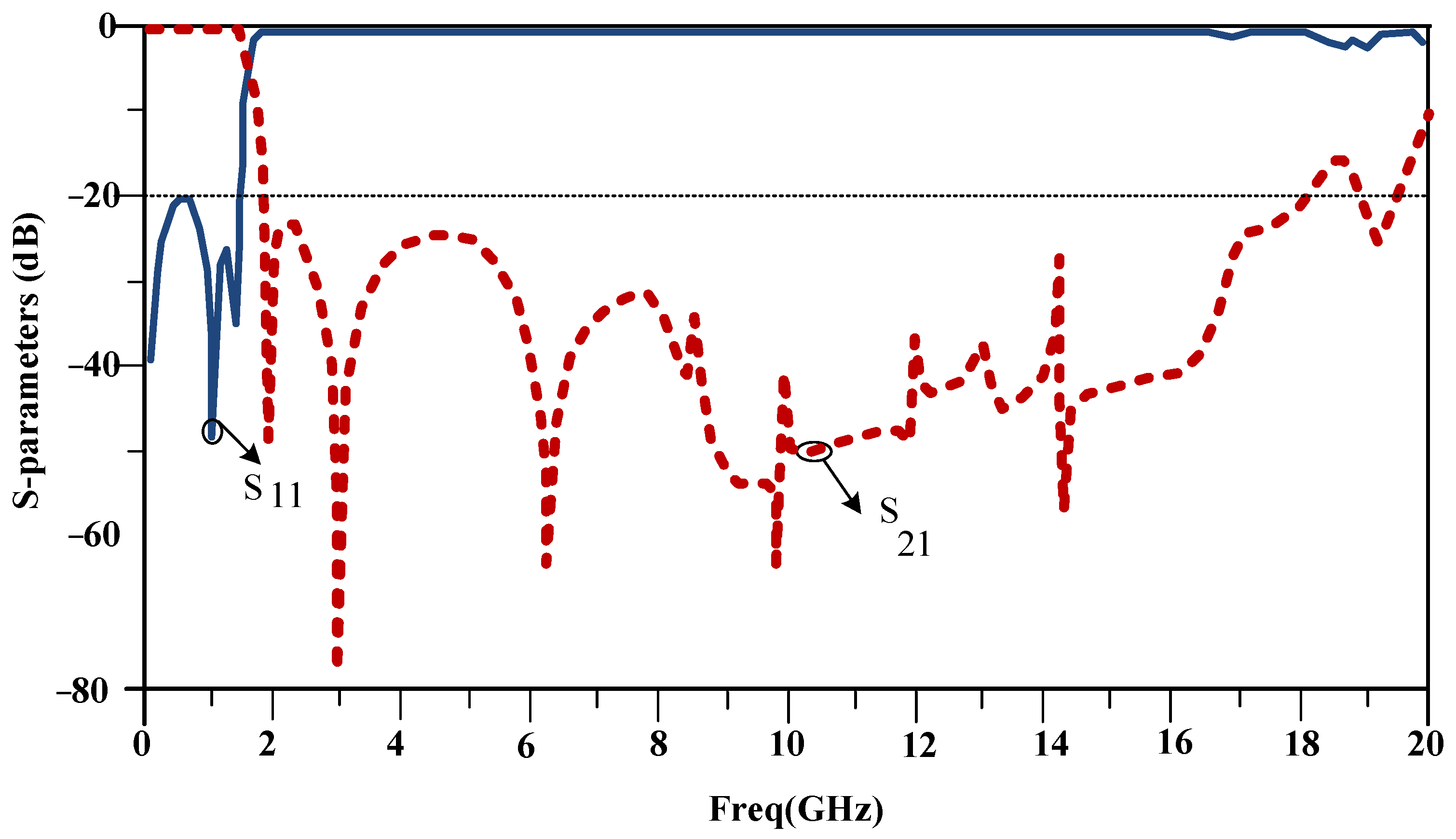
4.4. Proposed Low-Pass Filter
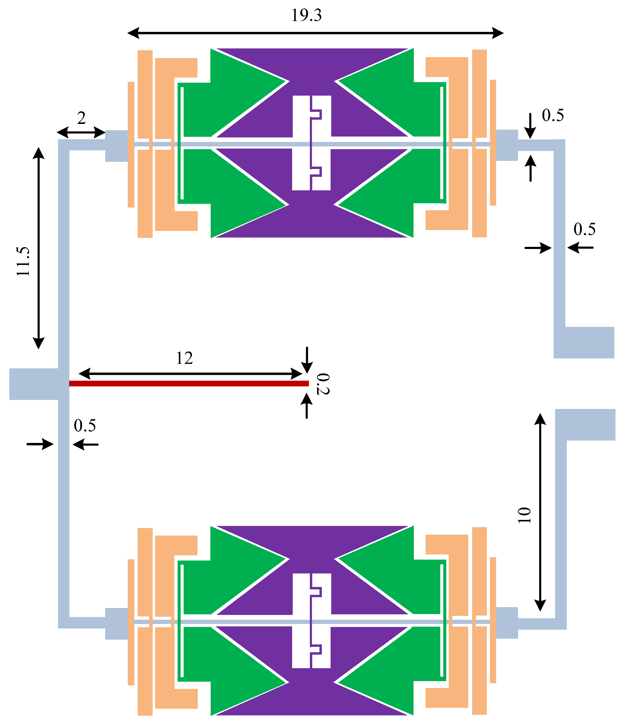
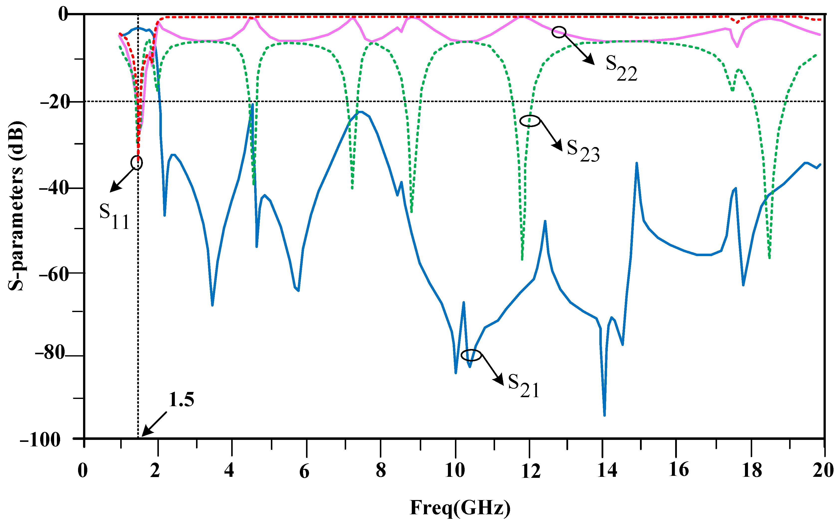
5. The Proposed Wilkinson Divider Design Process
6. Conclusions
Author Contributions
Funding
Data Availability Statement
Conflicts of Interest
References
- Alanazi, A.K.; Alizadeh, S.M.; Nurgalieva, K.S.; Nesic, S.; Grimaldo Guerrero, J.W.; Abo-Dief, H.M.; Eftekhari-Zadeh, E.; Nazemi, E.; Narozhnyy, I.M. Application of neural network and time-domain feature extraction techniques for determining volumetric percentages and the type of two phase flow regimes independent of scale layer thickness. Appl. Sci. 2022, 12, 1336. [Google Scholar] [CrossRef]
- Nazemi, E.; Feghhi, S.; Roshani, G.; Peyvandi, R.G.; Setayeshi, S. Precise void fraction measurement in two-phase flows independent of the flow regime using gamma-ray attenuation. Nucl. Eng. Technol. 2016, 48, 64–71. [Google Scholar] [CrossRef]
- Koziel, S.; Pietrenko-Dabrowska, A. Expedited feature-based quasi-global optimization of multi-band antenna input characteristics with jacobian variability tracking. IEEE Access 2020, 8, 83907–83915. [Google Scholar] [CrossRef]
- Calik, N.; Güneş, F.; Koziel, S.; Pietrenko-Dabrowska, A.; Belen, M.A.; Mahouti, P. Deep-learning-based precise characterization of microwave transistors using fully-automated regression surrogates. Sci. Rep. 2023, 13, 1445. [Google Scholar] [CrossRef]
- Jamshidi, M.; Moztarzadeh, O.; Jamshidi, A.; Abdelgawad, A.; El-Baz, A.S.; Hauer, L. Future of Drug Discovery: The Synergy of Edge Computing, Internet of Medical Things, and Deep Learning. Future Internet 2023, 15, 142. [Google Scholar] [CrossRef]
- Roshani, G.; Nazemi, E.; Roshani, M. Intelligent recognition of gas-oil-water three-phase flow regime and determination of volume fraction using radial basis function. Flow Meas. Instrum. 2017, 54, 39–45. [Google Scholar] [CrossRef]
- Hosseini, S.; Taylan, O.; Abusurrah, M.; Akilan, T.; Nazemi, E.; Eftekhari-Zadeh, E.; Bano, F.; Roshani, G.H. Application of wavelet feature extraction and artificial neural networks for improving the performance of gas–liquid two-phase flow meters used in oil and petrochemical industries. Polymers 2021, 13, 3647. [Google Scholar] [CrossRef]
- Roshani, S.; Azizian, J.; Roshani, S.; Jamshidi, M.; Parandin, F. Design of a miniaturized branch line microstrip coupler with a simple structure using artificial neural network. Frequenz 2022, 76, 255–263. [Google Scholar] [CrossRef]
- Cheng, K.-K.M.; Ip, W.-C. A novel power divider design with enhanced spurious suppression and simple structure. IEEE Trans. Microw. Theory Tech. 2010, 58, 3903–3908. [Google Scholar] [CrossRef]
- Roshani, S.; Yahya, S.I.; Mezaal, Y.S.; Chaudhary, M.A.; Al-Hilali, A.A.; Mojirleilani, A.; Roshani, S. Design of a Compact Quad-Channel Microstrip Diplexer for L and S Band Applications. Micromachines 2023, 14, 553. [Google Scholar] [CrossRef]
- Gu, J.; Sun, X. Miniaturization and harmonic suppression rat-race coupler using C-SCMRC resonators with distributive equivalent circuit. IEEE Microw. Wirel. Compon. Lett. 2005, 15, 880–882. [Google Scholar]
- Koziel, S.; Pietrenko-Dabrowska, A. On nature-inspired design optimization of antenna structures using variable-resolution EM models. Sci. Rep. 2023, 13, 8373. [Google Scholar] [CrossRef]
- Koziel, S.; Pietrenko-Dabrowska, A.; Ullah, U. Low-cost modeling of microwave components by means of two-stage inverse/forward surrogates and domain confinement. IEEE Trans. Microw. Theory Tech. 2021, 69, 5189–5202. [Google Scholar] [CrossRef]
- Koziel, S.; Pietrenko-Dabrowska, A. Constrained multi-objective optimization of compact microwave circuits by design triangulation and pareto front interpolation. Eur. J. Oper. Res. 2022, 299, 302–312. [Google Scholar] [CrossRef]
- Pietrenko-Dabrowska, A.; Koziel, S. Antenna modeling using variable-fidelity EM simulations and constrained co-kriging. IEEE Access 2020, 8, 91048–91056. [Google Scholar] [CrossRef]
- Moztarzadeh, O.; Jamshidi, M.; Sargolzaei, S.; Jamshidi, A.; Baghalipour, N.; Malekzadeh Moghani, M.; Hauer, L. Metaverse and Healthcare: Machine Learning-Enabled Digital Twins of Cancer. Bioengineering 2023, 10, 455. [Google Scholar] [CrossRef] [PubMed]
- Shum, K.M.; Xue, Q.; Chan, C.H. A novel microstrip ring hybrid incorporating a PBG cell. IEEE Microw. Wirel. Compon. Lett. 2001, 11, 258–260. [Google Scholar] [CrossRef]
- Oraizi, H.; Esfahlan, M.S. Miniaturization of Wilkinson power dividers by using defected ground structures. Prog. Electromagn. Res. Lett. 2008, 4, 113–120. [Google Scholar] [CrossRef]
- Woo, D.-J.; Lee, T.-K. Suppression of harmonics in Wilkinson power divider using dual-band rejection by asymmetric DGS. IEEE Trans. Microw. Theory Tech. 2005, 53, 2139–2144. [Google Scholar]
- Yu, X.; Sun, S. A novel wideband filtering power divider with embedding three-line coupled structures. IEEE Access 2018, 6, 41280–41290. [Google Scholar] [CrossRef]
- Roshani, S.; Yahya, S.I.; Roshani, S.; Rostami, M. Design and fabrication of a compact branch-line coupler using resonators with wide harmonics suppression band. Electronics 2022, 11, 793. [Google Scholar] [CrossRef]
- Coromina, J.; Velez, P.; Bonache, J.; Martín, F. Branch line couplers with small size and harmonic suppression based on non-periodic step impedance shunt stub (SISS) loaded lines. IEEE Access 2020, 8, 67310–67320. [Google Scholar] [CrossRef]
- Kumar, M.; Islam, S.N.; Sen, G.; Parui, S.K.; Das, S. Design of compact Wilkinson power divider and branch line coupler using hairpin based line. AEU-Int. J. Electron. Commun. 2019, 110, 152825. [Google Scholar] [CrossRef]
- Luo, M.; Xu, X.; Tang, X.-H.; Zhang, Y.-H. A Compact Balanced-to-Balanced Filtering Gysel Power Divider Using λg/2 Resonators and Short-Stub-Loaded Resonator. IEEE Microw. Wirel. Compon. Lett. 2017, 27, 645–647. [Google Scholar] [CrossRef]
- Li, Q.; Zhang, Y.; Wu, C.-T.M. High-selectivity and miniaturized filtering Wilkinson power dividers integrated with multimode resonators. IEEE Trans. Compon. Packag. Manuf. Technol. 2017, 7, 1990–1997. [Google Scholar] [CrossRef]
- Roshani, S.; Koziel, S.; Roshani, S.; Hashemi Mehr, F.S.; Szczepanski, S. Design and implementation of a dual-band filtering Wilkinson power divider using coupled T-shaped dual-band resonators. Energies 2022, 15, 1189. [Google Scholar] [CrossRef]
- Lotfi, S.; Roshani, S.; Roshani, S. Design of a miniaturized planar microstrip Wilkinson power divider with harmonic cancellation. Turk. J. Electr. Eng. Comput. Sci. 2020, 28, 3126–3136. [Google Scholar]
- Zhang, J.; Cui, B.; Gu, J.-Z.; Sun, X.-W. A harmonic suppressed Wilkinson power divider using complementary split ring resonators (CSRRs). J. Electromagn. Waves Appl. 2007, 21, 811–819. [Google Scholar] [CrossRef]
- Wen, P.; Ma, Z.; Liu, H.; Zhu, S.; Ren, B.; Song, Y.; Wang, X.; Ohira, M. Dual-band filtering power divider using dual-resonance resonators with ultrawide stopband and good isolation. IEEE Microw. Wirel. Compon. Lett. 2019, 29, 101–103. [Google Scholar] [CrossRef]
- Wang, Z.; Jang, J.-S.; Park, C.-W. Tri-band Wilkinson power divider using resonators. In Proceedings of the 2011 IEEE Radio and Wireless Symposium, Phoenix, AZ, USA, 7 March 2011; pp. 287–290. [Google Scholar]
- Shao, J.-Y.; Huang, S.-C.; Pang, Y.-H. Wilkinson power divider incorporating quasi-elliptic filters for improved out-of-band rejection. Electron. Lett. 2011, 47, 1288–1289. [Google Scholar] [CrossRef]
- Parandin, F.; Olyaee, S.; Kamarian, R.; Jomour, M. Design and simulation of linear all-optical comparator based on square-lattice photonic crystals. In Proceedings of the Photonics, Kuala Lumpur, Malaysia, 8–10 August 2022; p. 459. [Google Scholar]
- Parandin, F.; Moayed, M.; Heidari, F. All-optical diode for terahertz optical power rectification based on two-dimensional photonic crystals. Microelectron. J. 2023, 136, 105779. [Google Scholar] [CrossRef]
- Askarian, A.; Parandin, F. A novel proposal for all optical 1-bit comparator based on 2D linear photonic crystal. J. Comput. Electron. 2023, 22, 288–295. [Google Scholar] [CrossRef]
- Parandin, F.; Sheykhian, A. Design and simulation of a 2 × 1 All-Optical multiplexer based on photonic crystals. Opt. Laser Technol. 2022, 151, 108021. [Google Scholar] [CrossRef]
- Parandin, F.; Mahtabi, N. Design of an ultra-compact and high-contrast ratio all-optical NOR gate. Opt. Quantum Electron. 2021, 53, 666. [Google Scholar] [CrossRef]
- Parandin, F.; Sheykhian, A.; Bagheri, N. A novel design for an ultracompact optical majority gate based on a ring resonator on photonic crystal substrate. J. Comput. Electron. 2023, 22, 716–722. [Google Scholar] [CrossRef]
- Jamshidi, M.B.; Roshani, S.; Talla, J.; Roshani, S.; Peroutka, Z. Size reduction and performance improvement of a microstrip Wilkinson power divider using a hybrid design technique. Sci. Rep. 2021, 11, 7773. [Google Scholar] [CrossRef]
- Huang, W.; Liu, C.; Yan, L.; Huang, K. A miniaturized dual-band power divider with harmonic suppression for GSM applications. J. Electromagn. Waves Appl. 2010, 24, 81–91. [Google Scholar] [CrossRef]
- Kość, A.; Di Maria, A.; Limbach, M.; Horn, R.; Reigber, A. A 5 way lumped-elements Wilkinson power divider. In Proceedings of the 2013 7th European Conference on Antennas and Propagation (EuCAP), Gothenburg, Sweden, 8–12 April 2013; pp. 357–360. [Google Scholar]
- Wu, Y.; Liu, Y. Closed-form design method for unequal lumped-elements Wilkinson power dividers. Microw. Opt. Technol. Lett. 2009, 51, 1320–1324. [Google Scholar] [CrossRef]
- Kawai, T.; Nagano, K.; Enokihara, A. A 920MHz lumped-element Wilkinson power divider utilizing LC-ladder circuits. IEICE Trans. Electron. 2018, 101, 801–804. [Google Scholar] [CrossRef]
- Gao, N.; Wu, G.; Tang, Q. Design of a novel compact dual-band Wilkinson power divider with wide frequency ratio. IEEE Microw. Wirel. Compon. Lett. 2013, 24, 81–83. [Google Scholar] [CrossRef]
- Jamshidi, M.; Farhadi, R.; Jamshidi, M.; Shamsi, Z.; Naseh, S. Using a soft computing method for impedance modelling of li-ion battery current. Int. J. Adv. Intell. Paradig. 2020, 16, 18–29. [Google Scholar] [CrossRef]
- Shafiei, A.; Jamshidi, M.; Khani, F.; Talla, J.; Peroutka, Z.; Gantassi, R.; Baz, M.; Cheikhrouhou, O.; Hamam, H. A Hybrid Technique Based on a Genetic Algorithm for Fuzzy Multiobjective Problems in 5G, Internet of Things, and Mobile Edge Computing. Math. Probl. Eng. 2021, 2021, 9194578. [Google Scholar] [CrossRef]
- Nielsen, M.A. Neural Networks and Deep Learning; Determination Press: San Francisco, CA, USA, 2015; Volume 25. [Google Scholar]
- Bishop, C. Neural Networks for Pattern Recognition; Oxford University Press: New York, NY, USA, 1996. [Google Scholar]
- Goodfellow, I.; Bengio, Y.; Courville, A. Deep Learning; MIT Press: Cambridge, MA, USA, 2016. [Google Scholar]
- Haykin, S. Neural Networks and Learning Machines, 3/E; Pearson Education India: Delhi, India, 2009. [Google Scholar]
- Ting, S.-W.; Tam, K.-W.; Martins, R. Miniaturized microstrip lowpass filter with wide stopband using double equilateral U-shaped defected ground structure. IEEE Microw. Wirel. Compon. Lett. 2006, 16, 240–242. [Google Scholar] [CrossRef]
- Ma, K.; Yeo, K.S.; Lim, W.M. Ultra-wide rejection band lowpass cell. Electron. Lett. 2012, 48, 99–100. [Google Scholar] [CrossRef]
- Zhang, B.; Li, S.; Huang, J. Compact lowpass filter with wide stopband using coupled rhombic stubs. Electron. Lett. 2015, 51, 264–266. [Google Scholar] [CrossRef]
- Luo, S.; Zhu, L.; Sun, S. Stopband-expanded low-pass filters using microstrip coupled-line hairpin units. IEEE Microw. Wirel. Compon. Lett. 2008, 18, 506–508. [Google Scholar] [CrossRef]
- Mohra, A.S. Microstrip low pass filter with wideband rejection using opened circuit stubs and Z-slots defected ground structures. Microw. Opt. Technol. Lett. 2011, 53, 811–815. [Google Scholar] [CrossRef]
- Mandal, A.; Moyra, T. Compact low-pass filter (LPF) with wide harmonic suppression using interdigital capacitor. Frequenz 2023, 77, 1–8. [Google Scholar] [CrossRef]
- Mandal, A.; Moyra, T. Stub Resonator Based Compact Low-Pass Filter (LPF) with Wide Harmonic Suppression. Prog. Electromagn. Res. C 2022, 122, 31–40. [Google Scholar] [CrossRef]
- Zhang, F.; Li, C. Power divider with microstrip electromagnetic bandgap element for miniaturisation and harmonic rejection. Electron. Lett. 2008, 44, 422–424. [Google Scholar] [CrossRef]
- Karthikeyan, S.; Kshetrimayum, R. Compact, harmonic suppressed power divider using open complementary split-ring resonator. Microw. Opt. Technol. Lett. 2011, 53, 2897–2899. [Google Scholar] [CrossRef]
- He, J.; Feng Chen, Z.; Hai Yang, B.; Ying Xiong, M. Miniaturized microstrip Wilkinson power divider with capacitor loading. Microw. Opt. Technol. Lett. 2012, 54, 61–63. [Google Scholar] [CrossRef]


| W1 (mm) | W2 (mm) | W3 (mm) | W4 (mm) | L1 (mm) | fo (GHz) | ζ (dB/GHz) | BW (MHz) | RL (dB) | |
|---|---|---|---|---|---|---|---|---|---|
| Training Values | |||||||||
| Input Parameters | Output Parameters | ||||||||
| 1 | 10.7 | 2.2 | 0.2 | 0.1 | 18.7 | 1.52 | 38.2 | 5.46 | 23.2 |
| 2 | 10.7 | 1 | 0.2 | 0.1 | 18.7 | 1.52 | 36.1 | 4.97 | 22.3 |
| 3 | 10.7 | 1 | 0.2 | 0.2 | 18.7 | 1.61 | 29.2 | 5.61 | 22.2 |
| 4 | 10.7 | 1 | 0.1 | 0.2 | 18.7 | 1.49 | 22.9 | 6.43 | 15.8 |
| 5 | 11.3 | 1 | 0.1 | 0.2 | 18.7 | 1.43 | 23.5 | 6.45 | 16.8 |
| 6 | 11.3 | 2 | 0.1 | 0.2 | 18.7 | 1.38 | 23.8 | 6.46 | 17.9 |
| 7 | 10.7 | 2 | 0.1 | 0.2 | 18.7 | 1.43 | 27.9 | 6.49 | 16.9 |
| 8 | 10 | 2 | 0.1 | 0.2 | 18.7 | 1.53 | 26.9 | 6.5 | 15.3 |
| 9 | 10 | 1.6 | 0.1 | 0.2 | 18.7 | 1.52 | 25.6 | 6.5 | 14.9 |
| 10 | 10 | 1.6 | 0.2 | 0.2 | 18.7 | 1.65 | 27.6 | 5.78 | 19.4 |
| 11 | 10 | 1.6 | 0.2 | 0.2 | 16.3 | 1.69 | 54.1 | 6.16 | 23.2 |
| 12 | 10 | 1.6 | 0.2 | 0.1 | 16.3 | 1.61 | 34.8 | 5.7 | 23.2 |
| 13 | 9.5 | 1.6 | 0.2 | 0.1 | 16.3 | 1.7 | 28.4 | 5.88 | 21.8 |
| 14 | 9.5 | 1.4 | 0.2 | 0.1 | 16.3 | 1.67 | 25.5 | 6.36 | 21.4 |
| 15 | 9.5 | 1 | 0.2 | 0.1 | 16.3 | 1.71 | 34.1 | 5.8 | 20.8 |
| 16 | 8.9 | 1 | 0.2 | 0.1 | 16.3 | 1.76 | 27.2 | 5.83 | 19.3 |
| 17 | 8.3 | 1 | 0.2 | 0.1 | 16.3 | 1.83 | 31.4 | 5.74 | 17.7 |
| 18 | 8.3 | 0.8 | 0.2 | 0.1 | 16.3 | 1.87 | 38.5 | 5.7 | 17.5 |
| 19 | 7.7 | 0.8 | 0.2 | 0.1 | 16.3 | 1.92 | 24.1 | 5.68 | 16.1 |
| 20 | 7.7 | 0.6 | 0.2 | 0.1 | 16.3 | 1.95 | 30.7 | 5.66 | 15.9 |
| 21 | 7.7 | 0.6 | 0.2 | 0.1 | 15.3 | 2 | 25 | 5.9 | 17 |
| 22 | 8.2 | 0.6 | 0.2 | 0.1 | 15.3 | 1.93 | 31.1 | 6.18 | 17.9 |
| 23 | 8.2 | 0.8 | 0.2 | 0.1 | 15.3 | 1.93 | 32.4 | 6.1 | 18.2 |
| 24 | 8.5 | 0.8 | 0.2 | 0.1 | 15.3 | 1.87 | 27.1 | 5.92 | 19.2 |
| 25 | 8.5 | 1 | 0.2 | 0.1 | 15.3 | 1.86 | 27 | 5.88 | 19.5 |
| 26 | 8.9 | 1 | 0.2 | 0.1 | 15.3 | 1.81 | 27.2 | 5.96 | 20.7 |
| 27 | 9.2 | 1 | 0.2 | 0.1 | 15.3 | 1.79 | 34.1 | 5.97 | 21.4 |
| Testing Values | |||||||||
| Input Parameters | Output Parameters | ||||||||
| 1 | 9.2 | 0.6 | 0.2 | 0.1 | 15.3 | 1.77 | 33.5 | 5.96 | 21.1 |
| 2 | 9.2 | 1.1 | 0.2 | 0.1 | 15.3 | 1.76 | 33.3 | 6.05 | 21.6 |
| 3 | 9.6 | 1.1 | 0.2 | 0.1 | 15.3 | 1.72 | 34.3 | 6.1 | 22.8 |
| 4 | 10.1 | 1.1 | 0.2 | 0.1 | 15.3 | 1.67 | 29.6 | 6.48 | 25.1 |
| 5 | 10.1 | 1.5 | 0.2 | 0.1 | 15.3 | 1.58 | 34.3 | 6.55 | 25.9 |
| 6 | 10.1 | 0.9 | 0.2 | 0.1 | 15.3 | 1.64 | 28.9 | 6.05 | 24.7 |
| 7 | 11.1 | 0.9 | 0.2 | 0.1 | 15.3 | 1.54 | 27.8 | 6.11 | 28.6 |
| Validation Values | |||||||||
| Input Parameters | Output Parameters | ||||||||
| 1 | 9.9 | 2.2 | 0.2 | 0.1 | 18.7 | 1.52 | 30.58 | 5.02 | 22.2 |
| fo (GHz) Errors | ζ (dB/GHz) Errors | BW (MHz) Errors | RL (dB) Errors | |||||||||
|---|---|---|---|---|---|---|---|---|---|---|---|---|
| Training | Testing | Valid. | Training | Testing | Valid. | Training | Testing | Valid. | Training | Testing | Valid. | |
| MRE | 2.97 × 10⁻⁷ | 0.0226 | 0.0163 | 3.99 × 10⁻⁷ | 0.1464 | 0.1841 | 9.87 × 10⁻¹⁰ | 0.0203 | 0.0230 | 6.30 × 10⁻¹⁰ | 0.0188 | 0.0844 |
| RMSE | 3.01 × 10⁻⁶ | 0.0574 | 0.0163 | 1.09 × 10⁻⁴ | 5.4911 | 5.6301 | 9.01 × 10⁻⁹ | 0.1474 | 0.1157 | 2.07 × 10⁻⁸ | 0.8833 | 1.8727 |
| FOM | AF | NCS | SF | RSB | ζ | Refs. |
|---|---|---|---|---|---|---|
| 62,520 | 1 | 0.126 λg × 0.055 λg | 2.4 | 1.73 | 103.9 | [10] |
| 11,221 | 1 | 0.12 λg × 0.071 λg | 1.7 | 1.52 | 37 | [50] |
| 1159.3 | 1 | 0.12 λg × 0.063 λg | 1.6 | 1.66 | 5.3 | [51] |
| 27,142 | 1 | 0.12 λg × 0.1 λg | 3.5 | 1.61 | 57.8 | [52] |
| 4723 | 1 | 0.101 λg × 0.15 λg | 1 | 1.63 | 44 | [53] |
| 9065 | 1 | 0.111 λg × 0.091 λg | 1.5 | 1.65 | 37 | [54] |
| 7095 | 1 | 0.14 λg × 0.18 λg | 2 | 1.65 | 43 | [55] |
| 4464 | 1 | 0.23 λg × 0.22 λg | 2 | 1.45 | 62 | [56] |
| 49,843 | 1 | 0.15 λg × 0.081 λg | 2 | 1.63 | 185 | This work |
| Refs. | Frequency | Insertion Loss (IL) | Input Return Loss | Output Return Loss | Output Ports Isolation | Harmonics Suppression |
|---|---|---|---|---|---|---|
| [9] | 1 GHz | 0.25 dB | 40 dB | 31 dB | 32 dB | 2nd to 4th |
| [11] | 2.4 GHz | 0.65 dB | 22 dB | 22 dB | 20 dB | 2nd and 3rd |
| [57] | 1.8 GHz | 0.6 dB | 20 dB | 20 dB | 20 dB | 2nd and 3rd |
| [58] | 0.9 GHZ | 0.325 dB | 36 dB | N.A. | N.A. | 3rd |
| [59] | 1 GHz | 0.2 dB | 30 dB | 30 dB | 30 dB | 3rd to 5th |
| This work | 1.5 GHz | 0.1 dB | 35 dB | 30 dB | 32 dB | 2nd to 13th |
Disclaimer/Publisher’s Note: The statements, opinions and data contained in all publications are solely those of the individual author(s) and contributor(s) and not of MDPI and/or the editor(s). MDPI and/or the editor(s) disclaim responsibility for any injury to people or property resulting from any ideas, methods, instructions or products referred to in the content. |
© 2023 by the authors. Licensee MDPI, Basel, Switzerland. This article is an open access article distributed under the terms and conditions of the Creative Commons Attribution (CC BY) license (https://creativecommons.org/licenses/by/4.0/).
Share and Cite
Jamshidi, M.; Yahya, S.I.; Roshani, S.; Chaudhary, M.A.; Ghadi, Y.Y.; Roshani, S. A Fast Surrogate Model-Based Algorithm Using Multilayer Perceptron Neural Networks for Microwave Circuit Design. Algorithms 2023, 16, 324. https://doi.org/10.3390/a16070324
Jamshidi M, Yahya SI, Roshani S, Chaudhary MA, Ghadi YY, Roshani S. A Fast Surrogate Model-Based Algorithm Using Multilayer Perceptron Neural Networks for Microwave Circuit Design. Algorithms. 2023; 16(7):324. https://doi.org/10.3390/a16070324
Chicago/Turabian StyleJamshidi, Mohammad (Behdad), Salah I. Yahya, Saeed Roshani, Muhammad Akmal Chaudhary, Yazeed Yasin Ghadi, and Sobhan Roshani. 2023. "A Fast Surrogate Model-Based Algorithm Using Multilayer Perceptron Neural Networks for Microwave Circuit Design" Algorithms 16, no. 7: 324. https://doi.org/10.3390/a16070324
APA StyleJamshidi, M., Yahya, S. I., Roshani, S., Chaudhary, M. A., Ghadi, Y. Y., & Roshani, S. (2023). A Fast Surrogate Model-Based Algorithm Using Multilayer Perceptron Neural Networks for Microwave Circuit Design. Algorithms, 16(7), 324. https://doi.org/10.3390/a16070324