Article

Set-Point Control of a Spatially Distributed Buck Converter

by
Klaus Röbenack
1,*,† and
Stefan Palis
2,†
1
Institute of Control Theory, Faculty of Electrical and Computer Engineering, Technische Universität Dresden, 01062 Dresden, Germany
2
IT & Technology, Electrical Engineering, IU International University of Applied Sciences, 99084 Erfurt, Germany
*
Author to whom correspondence should be addressed.
These authors contributed equally to this work.
Algorithms 2023, 16(1), 55; https://doi.org/10.3390/a16010055
Submission received: 7 December 2022 / Revised: 4 January 2023 / Accepted: 9 January 2023 / Published: 13 January 2023
(This article belongs to the Collection Feature Papers in Algorithms)

Abstract

:
The classical buck converter is a very common DC–DC converter, which reduces an higher input supply voltage to a lower output load voltage. Replacing the inductor and the capacitor by a transmission line, we obtain a distributed buck converter, which can be described by partial differential equations. Therefore, we obtain a completely new class of model. This new topology can be used if the load is operated at some spatial distance from the power supply, where the power supply line is directly used as a reactive network element of the converter. In addition to the analysis and simulation we will also investigate the control of such a converter. In this contribution, we employ a discrepancy-based control technique. Approximating the theoretically derived feedback law yields an easy to implement sliding mode control scheme. The controller design is based on an ideal circuit model and verified by numerical simulation.

1. Introduction

The buck converter is a DC–DC converter transforming an input voltage into a lower output voltage [1,2]. The classical topology consists of an inductor and a capacitor combined with a diode and a transistor. Here, the diode and transistor resemble an ideal switch for the input voltage. Applying a pulse-width modulated signal to this switch results in a reduced apparent voltage, where the duty cycle, i.e., the ratio between closed switch position time and the period of the signal, determines the apparent output voltage level. The low pass character of the passive network of inductance and capacitance then results in a smoothing of the switching voltage.
Switched converters are a field of active research in power electronics [3]. DC–DC converters are used for consumer electronics, mobile devices, and photovoltaic applications [4,5]. For energy technology applications, the research focus is on multi-level three-phase converters [6]. Important goals are the design of converters are costs, energy efficiency, reliability, as well as the suppression of overshoots and higher harmonics. To achieve these goals, control has a special role to play [2,6,7].
In contrast to the described classical configuration, a new topology replacing the passive elements, i.e., the inductor and the capacitor, with a transmission line has been proposed in [8] and investigated further in [9,10,11]. This has been motivated by the transmission line model, which itself consists of distributed inductance and capacitor. The main advantage of this configuration lies in the reduced number of required elements, i.e., no inductor nor capacitor are required. If the load has a spatial distance from the power supply, a cable is needed anyway. We use this cable to replace the reactive network elements of the classical buck converter. In some applications, the use of a transmission line may be more advantageous than the use of an integrated inductor having a low inductance [12]. Disadvantages, however, are the significantly increased switching frequencies, due to the small capacitance and inductance values in conventional wires, and increased system complexity, due to the distributed nature of the transmission line. The connection of a boost converter to the load via a transmission line is investigated in [13]. Similarly, the connection of power converters by transmission lines is discussed in [14]. Note that transmission line models are also used in recent publications to model electric machines [15,16].
In the scientific literature there are a lot of works on the control of classical converter topologies. There, many control strategies are discussed, such as linear control (P/PI control, state feedback, output feedback [2]), as well as non-linear control (e.g., by exact linearization [17], flatness-based control [18], sliding mode [19] etc.). The circuit models of these converters use lumped elements. Unfortunately, the above mentioned control strategies cannot directly be applied to our converter circuit.
While previous work has addressed the modeling, analysis, and design of the distributed buck converter, this paper also addresses controller design. More precisely, the mathematical models for distributed buck converters under resistive and inductive load were derived in [8,9], respectively. In [11], a practical circuit realization was suggested and successfully tested. In this contribution, we will derive first control schemes taking into account the distributed system nature. More precisely, we employ a discrepancy-based control technique [20,21,22].
The paper is structured as follows: In Section 2 we derive models for the classical, as well as the distributed buck converter. The open-loop simulation is discussed in Section 3. To derive control laws for this model, the basic concepts of discrepancy-based control are presented in Section 4. Several different control strategies are derived in Section 5. We will discuss our results and suggest further directions of research in Section 6. In Section 7 we give a short summary and will draw some conclusions.

2. Physical Modeling

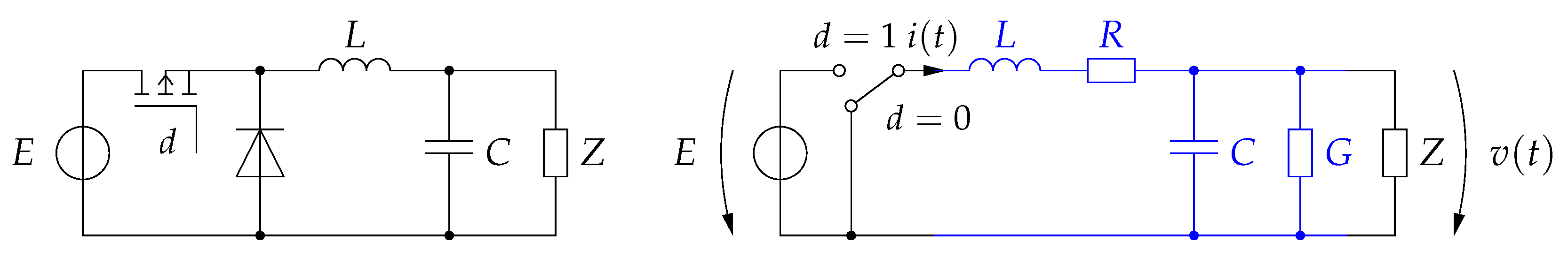
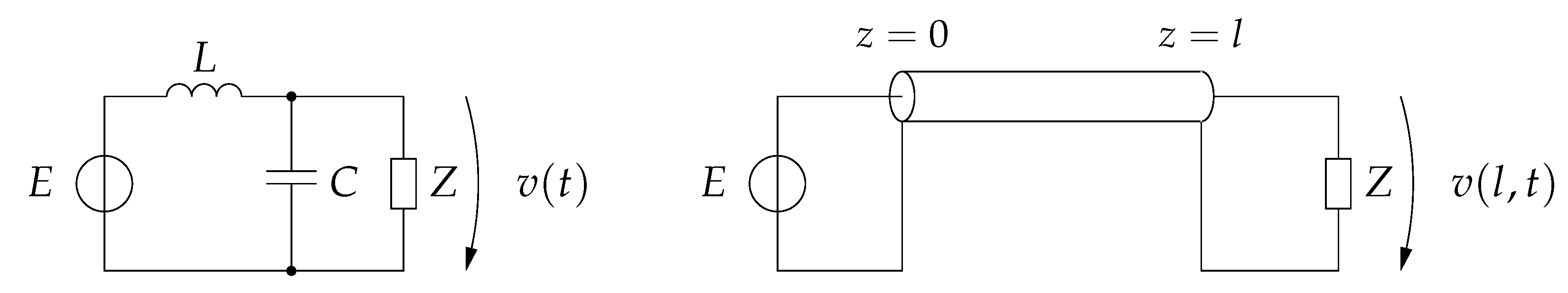
2.1. Classical Buck Converter

The schematics of a conventional buck converter is sketched in Figure 1 (left). The converter consists of two semiconductor elements (transistor, diode) and two reactive elements (inductor, capacitor). In this paper, the load is ohmic, i.e., a resistor with the resistance Z. The associated network model of the converter is shown in Figure 1 (right). The transistor with the freewheeling diode is modeled by an ideal switch with two positions d { 0 , 1 } . Therefore, the buck converter is a switching converter. The ohmic losses of the inductor and the capacitor are modeled by a resistance R and a conductance G, respectively. In Figure 1 (right), the resulting passive network to model the non-ideal reactive elements is drawn in blue color.
Based on the network model we can derive the circuits equations
L d i ( t ) d t + R i ( t ) + v ( t ) = E d ( t ) ,
C d v ( t ) d t + G v ( t ) + 1 Z v ( t ) = i ( t ) .
These equations form a system of first order ordinary differential equations (ODEs). In the model-theoretic context, system (1) is a lumped parameter model [23]. With the state vector x = ( x 1 , x 2 ) T = ( i , u ) T , we can rewrite the implicit system of ordinary differential equations as a two-dimensional state-space model
x ˙ ( t ) = A x ( t ) + b d ( t ) ,
where the system matrix  A and the input vector  b are given by
A = R L 1 L 1 C G + 1 / Z C , b = E L 0 .
The circuit Equation (1) can be transformed from time to frequency domain using Laplace transform
s L + R 1 1 s C + G + 1 Z M ( s ) I ( s ) V ( s ) = E 0 D ( s ) ,
where we use capital letters for the transformed signals. The characteristic polynomial of this system
det M ( s ) = L C s 2 + L G + R C + L Z s + 1 + R G + 1 Z
is a second order polynomial. For meaningful physical parameter values (i.e., L , C , Z > 0 and R , G 0 ), it is a Hurwitz polynomial corresponding to a damped harmonic oscillator. In the lossless case, i.e., R = 0 and G = 0 , the characteristic polynomial simplifies to
det M ( s ) = L C s 2 + L Z s + 1 .
This polynomial has real roots if, and only if, 4 C Z 2 L .
For a converter described by (2), one may consider three types of models [1,18,24,25]. In the switched model, the input signal d { 0 , 1 } takes discrete values corresponding to the positions of the switch. In practice, the system is excited via pulse-width modulation (PWM) with a fixed switching period T. If the average of all signals is taken over one switching period, one obtains the averaged model. The averaged model has the same structure as the original system (2). The averaged input signal d is called duty ratio or duty cycle with values from the interval d [ 0 , 1 ] . For T 0 the averaged model is transformed into the continuous model. In our simulations we will use the switched model with PWM excitation.
To compute the equilibrium x 0 = ( i 0 , u 0 ) T of the averaged model, we set x ˙ 0 . From (2) we obtain
x 0 = A 1 b d = E G R Z + Z + R G Z + 1 Z d E Z E d
for the lossless case with R = 0 and G = 0 . With d [ 0 , 1 ] and u 0 = E d , the operating point of the output voltage lies in the range between 0 and E, i.e., the buck converter can reduce the input voltage E to an average output voltage 0 u 0 E .

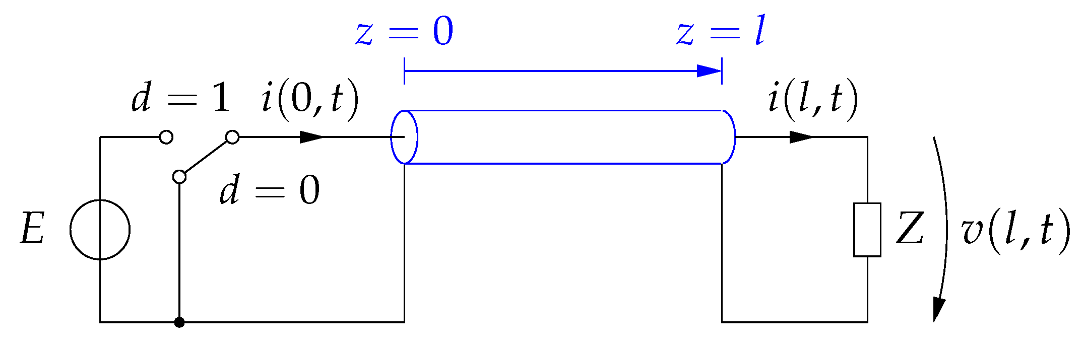
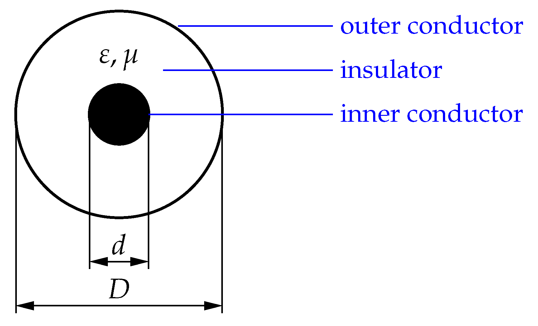
2.2. Distributed Buck Converter

The passive elements of the classical buck converter network model drawn in Figure 1 (right) with blue color can be interpreted as a lumped parameter model of a transmission line. Replacing these elements by a transmission line results in the distributed buck converter shown in Figure 2, see [8,11]. On the left side of the transmission line, we have the electronic switch (single pole changeover). The ohmic load is on the right side of the transmission line.
The transmission line can be modeled by the telegrapher’s equations [26,27]:
z v ( z , t ) + L t i ( z , t ) + R i ( z , t ) = 0 ,
z i ( z , t ) + C t v ( z , t ) + G v ( z , t ) = 0 .
The current i and the voltage u do not only depend on the time, but also on the spatial position z ( 0 , l ) , where l denotes the length of the transmission line (see Figure 2). In this model, the lumped parameters L, C, R, and G are replaced by distributed parameters L , C , R , G that describe inductance, capacitance, resistance, and conductance per length, respectively. These equations form a system of first order partial differential equations (PDEs). In a control-theoretic context, this system is also called a distributed parameter model [23,28].
The dynamics of the transmission line is influenced by the boundary conditions. On the left boundary, i.e., at z = 0 , we have the switched input voltage E d ( t ) . On the right boundary, i.e., at z = l , we have the ohmic load Z. This leads to the Dirichlet boundary conditions
v ( 0 , t ) = E d ( t ) ,
v ( l , t ) Z i ( l , t ) = 0 .
Overall, Equation (4) constitute a boundary value problem.
Next, we want to transform the PDE model of the transmission line into frequency domain. Applying the Laplace transform w.r.t. time t to Equation (4a,b) yields
z V ( z , s ) + ( s L + R ) I ( z , s ) = 0 ,
z I ( z , s ) + ( s C + G ) V ( z , s ) = 0 .
where we assume vanishing initial values, i.e., i ( · , 0 ) = 0 and v ( · , 0 ) = 0 . With this transformation, the PDEs are transformed into a system of first order linear homogeneous ODEs. Using an exponential function e λ z (Euler ansatz), system (5) is associated with the system matrix
M = s L + R λ λ s C + G
having the characteristic equation
det ( M ) = ( s L + R ) ( s C + G ) λ 2 = 0 .
In the lossless case, i.e., R = 0 and G = 0 , the characteristic equation simplifies to
det ( M ) = L C s 2 λ 2 = 0 with λ 1 , 2 = ± s L C .
The transmission line can then also be described by the characteristic impedance  Z 0 = L / C and the propagation delay τ = L C .
Remark 1.
The characteristic polynomials (3) and (6) are both second order polynomials, but have a different structure. Although the reactive elements of the classical converter are assumed to be lossless, we have a damping term in (3) resulting from the load resistance. The characteristic polynomial (6) resulting from the lossless transmission line has no damping term at all, because the damping due to the load is not part of the PDE itself but of the boundary condition (4d).
Remark 2.
In our modeling, we considered ohmic losses of the reactive elements and the transmission line, respectively. However, we assumed that the switching is ideal. In practice, the switch is usually implemented by a transistor together with a freewheeling diode, but could also be realized with two transistors. In Figure 1 (left), we used a MOSFET as an active element. Alternatively, one could also use an insulated-gate bipolar transistor (IGBT) or a gate turn-off thyristor (GTO). We assume that the transistor is operated as a switch. When the transistor is on, we model it as a short circuit. We model a switched-off transistor as an open circuit. In electronics, we neither have zero nor infinite resistance. This behavior can be taken into account with additional resistive elements in the model. The switching speed, characterized by the rise and fall times, can be modeled with additional capacitances. These effects of non-ideal behavior can be easily simulated with a circuit simulator. On the other hand, a highly detailed simulation model is often to complicated for controller design. Therefore, controller design is usually carried out with a much simplified or idealized model, e.g., [2,17,18,19,29]. The deviations of the actual system from the simplified nominal model can be taken into account in a robust controller design by means of uncertainty models [30].

3. Open-Loop Simulation

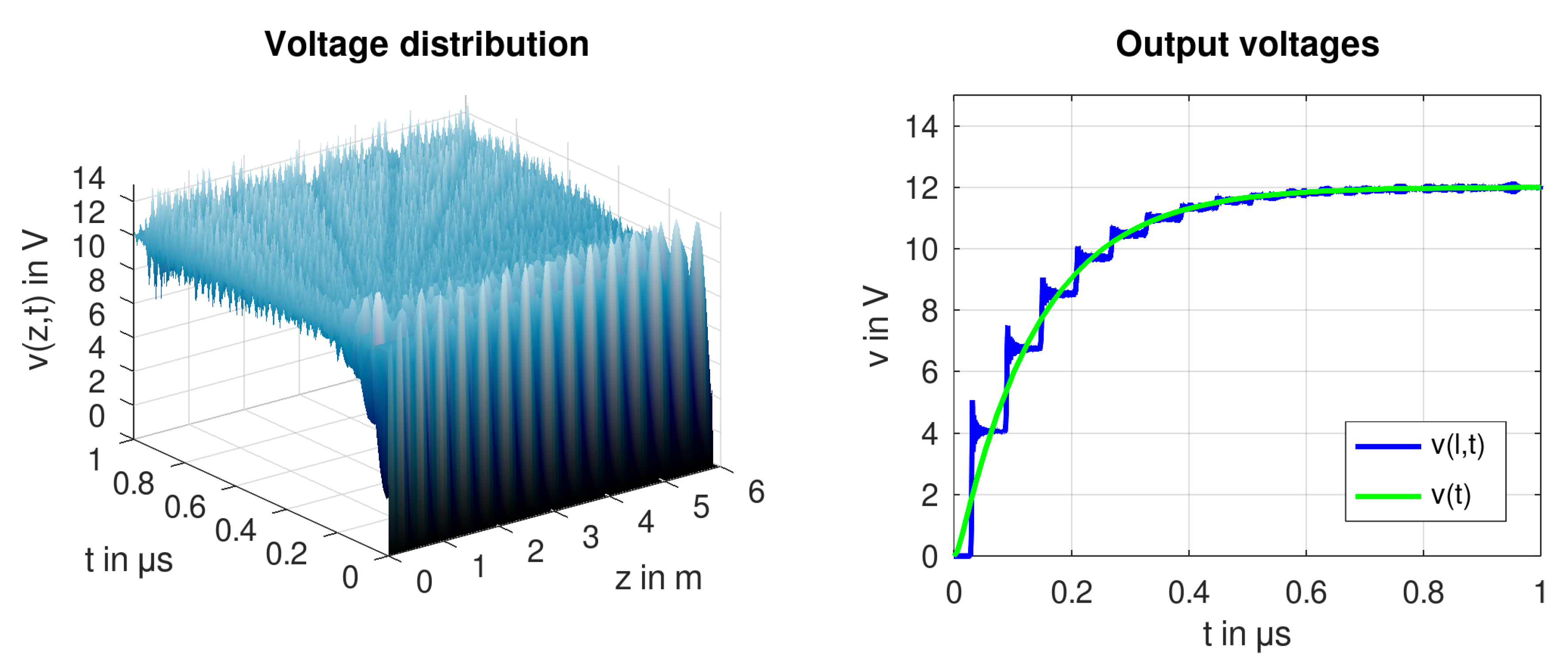
3.1. Simulation Setup

For the distributed converter we used the same setup as in [11]. In particular, the transmission line consists of l = 6   m coaxial cable RG 58 C/U [31]. Figure 3 shows the cross-section of the coaxial cable. The inner and outer conductors are made of copper. Since copper is a very good conductor, we assume the lossless case with R = 0   Ω / m . For the insulation (dielectric), polyethylene is used. Assuming perfect insulation we set G = 0   S / m . Based on the geometry, capacitance and inductance per length can be computed by
C = 2 π ε 1 ln D d and L = μ 2 π ln D d ,
where ε is the permittivity and μ is the permeability. Note that polyethylene has a relative permittivity ε r 2.3 and a relative permeability μ r 1 . The numerical values of the relevant parameters of the coaxial cable are listed in Table 1.
To simulate the distributed buck converter, we used the method of lines (MOL) to discretize Equation (4a,b) w.r.t. the spatial direction [32,33,34]. The line between z = 0   m and z = 6   m was divided into 100 equidistant points. This discretization of the spatial voltage and the current distribution results in a 200-dimensional state-space system. The numerical simulation was carried out with the open source tool GNU Octave [35] using the function ode45. This ODE solver employs the explicit Dormand–Prince method, which is a special Runge–Kutta method of order ( 4 , 5 ) .
We also want to compare the behavior of the distributed converter with the classical buck converter. There, we also assumed the lossless case, i.e., R = 0   Ω and G = 0   S . For the reactive lumped elements we used the overall capacitance C = l · C = 600   p F and the inductance L = l · L = 1446   n H . For the simulation, the state-space system (2) was also solved with the function ode45.

3.2. Transient Motion into the Steady-State

We excite the converters with a constant input voltage E = 12   V setting d 1 . The setup is shown in Figure 4. All initial values were set to zero. The results of the numerical simulations are shown in Figure 5. For the distributed converter, the wave propagation of the voltage v ( z , t ) w.r.t. time and space is shown in Figure 5 (left). The output voltage v ( l , t ) on the right boundary of the distributed converter and output voltage v ( t ) of the classical converter are shown in Figure 5 (right). In theory, the output voltage should be a piecewise constant function resulting from the superposition of travelling waves. The oscillations between different voltage levels are a well-known artefact occurring in the numerical solution of hyperbolic PDEs [32] resulting from the approximation of spatial derivatives. These oscillations could be reduced with more sophisticated difference schemes schemes [36,37].
The voltage of the classical buck converter increases at once and converges continuously to the steady-state value of 12   V . For the distributed converter, we see no reaction in the voltage until the propagating wave reaches the right boundary at t = τ l 30   n s . The voltage increases with each reflected wave and converges also to the steady-state value of 12   V . Although the numerical simulation of both converters yields approximately the same signal values, the output curves are qualitatively different.

3.3. Transient Motion under Pulse-Width Modulation

Now, we excite the converters with a PWM signal. We use E = 12   V and a duty ratio d = 0.5 , which should result in an average output voltage of E d = 6   V . For the PWM switching period T we used integer multiples of the delay time τ l 30   n s . The simulation results are shown in Figure 6. The output voltage v ( t ) of the classical converter oscillates around 6   V . For smaller PWM switching times (i.e., higher switching frequencies) the voltage ripples become smaller. Among the simulation scenarios, the best result is obtained with T = τ l .
The situation is different in case of the distributed converter. For T = τ l and T = 2 τ l , the output voltage sweeps the full range from 0   V to 12   V . For a switching period with a greater multiple of the delay time τ l , we obtain smaller voltage ripples. The smallest voltage ripples occur with T = 4   τ l , where the travelling waves partially compensate each other. This is consistent with the findings reported in [11]. In contrast to the classical converter, the voltage ripples cannot be arbitrarily reduced.

4. Discrepancy-Based Control

Discrepancy-based control [22] is a control approach for distributed parameter systems. The main idea is the investigation of the control problem in a generalized stability setting, stability with respect to two discrepancies [20,21]. In the following, the main concepts according to [22] are presented.
Consider a dynamical system with a solution φ ( · , t ) and an equilibrium at zero φ 0 = 0 . The discrepancy ρ ( φ ( · , t ) , t ) is than the generalized distance between the solution φ ( · , t ) and the equilibrium φ 0 .
Definition 1
(Discrepancy [21]). A discrepancy is a real valued functional ρ = ρ ( φ · , t , t with the following properties
1. 
ρ ( φ , t ) 0 ,
2. 
ρ ( 0 , t ) = 0 ,
3. 
For an arbitrary process φ = φ ( · , t ) the real valued functional ρ ( φ ( · , t ) , t ) is continuous with respect to t.
Obviously, the discrepancy is a generalization of more traditional distance measures as the L p - and the L - norm.
To account for deviations of the initial state φ ( . , 0 ) from the equilibrium φ 0 , a second time independent discrepancy ρ 0 fulfilling some continuity condition can be used. Stability with respect to two discrepancies can then be defined as follows.
Definition 2
(Stability with respect to two discrepancies ρ and ρ 0 [21]). The equilibrium φ 0 = 0 is stable in the sense of Lyapunov with respect to the two discrepancies ρ and ρ 0 for all t t 0 if for every ε > 0 and t 0 0 there exists a δ = δ ( ε , t 0 ) > 0 , such that for every process φ ( · , t ) with ρ 0 < δ ( ε , t 0 ) it follows that ρ < ε for all t t 0 . If in addition lim t ρ = 0 , then the equilibrium φ 0 is called asymptotically stable in the sense of Lyapunov with respect to the two discrepancies ρ and ρ 0 .
To introduce an according Lyapunov functional the notion of positive definiteness with respect to a discrepancy has to be introduced.
Definition 3
(Positive definiteness with respect to a discrepancy ρ [21]). A functional V = V φ , t is positive definite with respect to a discrepancy ρ, if V 0 and V 0 , t = 0 for all φ with ρ ( φ , t ) < and for every ε > 0 there exists a δ = δ ( ε ) > 0 , such that V δ ( ε ) for all φ with ρ φ , t ε .
The basis for the discrepancy-based control design, is given by the following theorem providing a connection between (asymptotic) stability with respect to two discrepancies and the existence of an according Lyapunov functional V.
Theorem 1
(Lyapunov functional [21]). The process φ with the equilibrium φ 0 = 0 is stable with respect to the two discrepancies ρ and ρ 0 if, and only if, there exists a functional V = V [ φ , t ] positive definite with respect to the discrepancy ρ, continuous at time t = t 0 with respect to ρ 0 at ρ 0 = 0 and not increasing along the process φ, i.e., V ˙ 0 . The process is asymptotically stable if in addition lim t V = 0 .
As will be shown in the next section, the main step for a discrepancy-based control design is to define an appropriate discrepancy, which allows for a simple Lyapunov-based control design and incorporates process knowledge.

5. Closed-Loop Control of the Distributed Buck Converter

5.1. Continuous Control Mode

In the following it will be assumed that the voltage at the beginning of the transmission line can be continuously actuated and will hence serve as a control handle. In order to design an appropriate control law, the mean current deviation from the desired current distribution i d ( z , t ) will be used as an error measure.
e = 0 l ( i d i ) d z
This results in the following discrepancy ρ with the according quadratic control-Lyapunov functional V.
V = ρ = 1 2 e 2
To derive a control law stabilizing the buck converter in continuous voltage control mode the time derivative of the control-Lyapunov functional V along the system trajectory is taken:
V ˙ = 0 l ( i d i ) d z · 0 l i d t + 1 L v z + R i d z
= 0 l ( i d i ) d z · 0 l i d t d z + 1 L v 0 l + R L 0 l i d z
= 0 l ( i d i ) d z · 0 l i d t d z + R L 0 l i d z + 1 L v ( l , t ) v ( 0 , t ) .
Here, the input voltage v ( 0 , t ) on the left boundary has to be chosen such that the time derivative of the control-Lyapunov functional V is negative definite in order to achieve a stable closed-loop system. One possible choice is the following compensating control law
v ( 0 , t ) = v ( l , t ) + L 0 l i d t d z + R 0 l i d z + K · L 0 l ( i d i ) d z .
The first term on the right hand side of Equation (10) is the output voltage on the right boundary. The second and third term describe the voltage drop along the line resulting from the inductance and resistance distribution with regard to the current deviation. The fourth term is the correction term with the control gain K > 0 . Applying the control law (10) then results in an exponential converging Lyapunov functional V and, thus, achieves exponential stability with respect to the discrepancy ρ :
V ˙ = K 0 l ( i d i ) d z 2 = 2 K V .
Now, we assume that the desired current i d is constant. In addition, we consider a lossless transmission line, i.e., R = 0 . However, we can set this control signal in relation to the constant input voltage to obtain the duty ratio
d ( t ) = 1 E v ( l , t ) + K · L 0 l ( i d i ) d z ,
which imposes the digital PWM signal to the distributed buck converter via the boundary condition (4c).

5.2. Discontinuous Control Mode

As has been described before, the actuation for the buck converter is achieved via a switching element. The described continuous operation modes can be seen as a certain approximation assuming high switching frequencies. However, for a practical application it is preferable to actuate the switch directly. A simple switching control law based on the sign of the mean current deviation along the transmission line can be derived from the time derivative (9) of the control-Lyapunov functional (8):
d ( t ) = 1 if 0 l ( i d i ) d z > 0 , 0 if 0 l ( i d i ) d z 0 .
In Equation (13), d { 0 , 1 } is the switch signal depicted in Figure 2, i.e., d = 0 switch open and d = 1 closed switch. The according voltage at the receiving end of the transmission line hence becomes
v ( 0 , t ) = E if 0 l ( i d i ) d z > 0 , 0 if 0 l ( i d i ) d z 0 ,
where the reference current i d is assumed to be constant as in Section 5.1.
To prove the closed-loop stability applying the control law (14), the time derivative (9) of the control-Lyapunov functional (8) is investigated for two cases: positive and negative including zero mean current deviation. In case of a positive mean current deviation, i.e., 0 l ( i d i ) d z > 0 , the switch is closed and the input voltage E is applied to the sending end of the transmission line v ( 0 , t ) = E . Assuming that the input voltage is sufficiently high to compensate for the transmission losses, which is an obvious design requirement, the following inequality holds:
v ( l , t ) + L 0 l i d t d z + R 0 l i d z E
Due to this inequality (15) the time derivative (9) of the control-Lyapunov functional (8) is in case of a positive mean current deviation less or equal than zero:
V ˙ = 0 l ( i d i ) d z 1 L v ( l , t ) + R 0 l i d z E 0 .
For a negative or vanishing mean current deviation 0 l ( i d i ) d z 0 , the switch is open and no input voltage is applied v ( 0 , t ) = 0 . As both current and voltage are assumed to be non-negative the following inequality results:
v ( l , t ) + R 0 l i d z 0 .
Therefore, the time derivative (9) of the control-Lyapunov functional (8) is again less or equal than zero:
V ˙ = 0 l ( i d i ) d z 1 L v ( l , t ) + R 0 l i d z 0 ,
which proves stability in the sense of Lyapunov with respect to the discrepancy ρ .

5.3. Implementation by Approximation

Both control laws (12) and (13) derived in Section 5.1 and Section 5.2 contain the integral
0 l ( i d i ) d z
which is defined on a spatially distributed signal. The integral (19) is essentially the mean current deviation along the transmission line. In practice, it is not feasible to measure the current distribution along the transmission line. To overcome this problem three very simple approximations, which can be applied to approximate this integral, are: the left, the midpoint, and the right rectangular approximations.
0 l ( i d i ( z , t ) ) d z ( i d i ( 0 , t ) ) · l ( left rectangular approximation ) ( i d i ( l / 2 , t ) ) · l ( midpoint rectangular approximation ) ( i d i ( l , t ) ) · l ( right rectangular approximation )
Using the left rectangular approximation would only require the signal value i ( 0 , t ) on the left boundary of the transmission line, where the semiconductor switch and the controller are located. Other approximations, such as the midpoint and the right rectangular approximation, as well as trapezoidal or Simpson’s rule would require current measurements with a spatial distance from the controller. Therefore, the left rectangular approximation is preferable and will be used in the following. Since l > 0 , the left rectangular approximation applied to (13) yields the control law
d ( t ) = 1 if ( i d ( 0 ) i ( 0 , t ) ) > 0 , 0 if ( i d ( 0 ) i ( 0 , t ) ) 0 .
To simulated the controlled system we use the parameters as discussed in Section 3. The desired output voltage is set to v d = 6   V . This corresponds to a desired current
i d = u d Z = 6   V 10   Ω = 0.6   A
required by the control law (21). The simulation results are shown in Figure 7, where the initial (discretized) voltage and current distribution were set to zero. In the beginning, the current i ( 0 , t ) on the left boundary is less then the desired current i d . In particular, we have
i ( 0 , t ) = E Z 0 = 12   V 50   Ω = 0.24   A for t < 2   τ l 60   n s
until the reflected wave reaches the left boundary. According to (21), the switch is in the position d = 1 , see Figure 7 (top left). When the current exceeds the desired current at t 0.12   μ s , the switch changes between the positions d = 0 and d = 1 at a very high frequency as shown in Figure 7 (bottom left). After the transients, we have very small voltage ripples in the output voltage v ( l , t ) , see Figure 7 (top right).
Remark 3.
The (discontinuous) two-point control laws (13) and (21) can be regarded as sliding mode control [19,38] or, more specifically, as discrepancy-based sliding mode control [39]. As a matter of fact, sliding mode is a common approach to control power converters [17,19,29]. In a classical sliding mode control, we would have a (theoretically) infinite switching frequency when the sliding surface is reached. In practice, the switching is not perfect, resulting in a high-frequency control action known as chattering [38,40]. When the control signal d given by (21) changes, the voltage wave would travel forward an be reflected on the right boundary. When the backward travelling wave reaches the left bound, the original control action may result in the next change of the control signal. This consideration should result in the switching frequency f = 1 / 2   τ l . Due to numerical deviations from the exact solution we also see a high frequency control action for the time between the reflected waves, see Figure 7 (bottom left) starting at t 0.12   μ s . This behavior is also expected in practice due to noise.

6. Discussion

The current investigations on the control of the distributed buck converter can be seen as a proof of concept, which, for several reasons, is not yet ready for a technical application. For example, the coaxial cable used here is comparatively expensive and not suited for power electronics. The short length of the transmission line results in a high switching frequency. In a further realization, the coaxial cable could be replaced by twisted pair cable. If the load is operated at a much larger distance from the power supply, such as in power grid applications, we would obtain a significantly lower switching frequency.
The control law (21) used in the simulation is easy to implement and fulfills the control goal as shown in Figure 7. The control laws (12) and (13) require the spatial integral of current deviation along the transmission line. These integrals can be computed in a simulation, but not directly be obtained in a practical realization. On the one hand, one could investigate how this integral can be estimated by means of observers, see [41,42]. On the other hand, it should be possible to replace the spatial integration by a time integration, because the solution of the telegrapher’s equation is a superposition of travelling waves. In addition, a more advanced control strategy could include an identification of the transmission lines parameters, cf. [43].
There are two main approaches to control distributed systems, namely early and late lumping. In early lumping, the system is discretized first and the controller is designed afterward for the (finite dimensional) approximation. This approach can lead to an unstable control loop if important system properties are lost by the approximation. In the late-lumping approach, the controller is designed for the (infinite dimensional) distributed system. Then, the controller is discretized for the implementation. The control strategy suggested in Section 5.3 can be interpreted as late lumping approach.
In the article, the converter was examined exclusively with resistive load. For practical applications, e.g., for electric drives or power grids, an inductive load with ohmic losses should be investigated [9,10]. In particular, voltage ripples caused by switching converters may reduce the durability of power grids and the attached electrical drives [15,16,44,45].
Further research could also be devoted to extend the concept of a (spatially) distributed buck converter to other switched DC–DC converter topologies such as boost and buck-boost converters, as well as to DC–AC, AC–DC, and three-phase power converters [1,2].

7. Summary and Conclusions

The power electronic part of a buck converter can already be realized with four components, namely with two semiconductor elements and two passive components. If you include the supply line between power supply and load, you can also spare the passive components, coil and capacitor. However, this change in circuit topology also results in qualitatively different behavior, both in open and closed loop. In this contribution, we investigated the impact of the switching time on voltage ripples in more detail. To derive an appropriate control algorithm, which allows for stabilization of a given set-point, a discrepancy-based design procedure has been applied. Here, the main steps are: choice of an appropriate generalized error measure (the discrepancy) and derivation of a stabilizing control law, which guarantees stability in the sense of Lyapunov with respect to the chosen discrepancy. For an implementation in a micro controller additional approximations of the derived control algorithm have been proposed.

Author Contributions

Conceptualization, K.R. and S.P.; methodology, K.R. and S.P.; software, K.R. and S.P.; formal analysis, K.R. and S.P.; writing—original draft preparation, S.P.; writing—review and editing, K.R.; visualization, K.R. and S.P. All authors have read and agreed to the published version of the manuscript.

Funding

This research received no external funding.

Data Availability Statement

The source code of the simulations performed in this study is available on request from the corresponding author.

Conflicts of Interest

The authors declare no conflict of interest.

Abbreviations

The following abbreviations are used in this manuscript:
ODEOrdinary differential equation
PDEPartial differential equation
PWMPulse-width modulation
MOLMethod of lines
MOSFET    metal-oxide-semiconductor field-effect transistor

References

  1. Erickson, R.W.; Maksimovic, D. Fundamentals of Power Electronics; Springer Science & Business Media: Cham, Switzerland, 2007. [Google Scholar] [CrossRef]
  2. Bacha, S.; Munteanu, I.; Bratcu, A.I. Power Electronic Converters Modeling and Control; Springer: London, UK, 2014. [Google Scholar]
  3. Bose, B.K. Recent advances in power electronics. IEEE Trans. Power Electron. 1992, 7, 2–16. [Google Scholar] [CrossRef]
  4. Taghvaee, M.; Radzi, M.; Moosavain, S.; Hizam, H.; Marhaban, M.H. A current and future study on non-isolated DC–DC converters for photovoltaic applications. Renew. Sustain. Energy Rev. 2013, 17, 216–227. [Google Scholar] [CrossRef]
  5. Kumar, G.K.; Elangovan, D. Review on fault-diagnosis and fault-tolerance for DC–DC converters. IET Power Electron. 2020, 13, 1–13. [Google Scholar] [CrossRef]
  6. Levi, E.; Bodo, N.; Dordevic, O.; Jones, M. Recent advances in power electronic converter control for multiphase drive systems. In Proceedings of the 2013 IEEE Workshop on Electrical Machines Design, Control and Diagnosis (WEMDCD), Paris, France, 11–12 March 2013; pp. 158–167. [Google Scholar] [CrossRef]
  7. Bärnklau, H.; Gensior, A.; Rudolph, J. A Model-Based Control Scheme for Modular Multilevel Converters. IEEE Trans. Ind. Electron. 2013, 60, 5359–5375. [Google Scholar] [CrossRef]
  8. Huang, C.; Woittennek, F.; Röbenack, K. Steady-state analysis of a distributed model of the buck converter. In Proceedings of the European Conference on Circuit Theory and Design (ECCTD), Dresden, Germany, 8–12 September 2013; pp. 1–4. [Google Scholar] [CrossRef]
  9. Huang, C.; Woittennek, F.; Röbenack, K. Distributed parameter model of the buck converter with constant inductive load. IFAC-PapersOnLine 2015, 48, 691–692. [Google Scholar] [CrossRef]
  10. Della Torre, F.; Morando, A.P.; Todeschini, G. Three-phase distributed model of high-voltage windings to study internal steep-fronted surge propagation in a straightforward transformer. IEEE Trans. Power Deliv. 2008, 23, 2050–2057. [Google Scholar] [CrossRef]
  11. Röbenack, K.; Herrmann, R. Analysis, Simulation and Implementation of a Distributed Buck Converter. In Proceedings of the 26th International Conference on System Theory, Control and Computing (ICSTCC), Sinaia, Romania, 19–21 October 2022; pp. 213–218. [Google Scholar] [CrossRef]
  12. Wibben, J.; Harjani, R. A High-Efficiency DC–DC Converter Using 2 nH Integrated Inductors. IEEE J. Solid-State Circuits 2008, 43, 844–854. [Google Scholar] [CrossRef]
  13. Daafouz, J.; Tucsnak, M.; Valein, J. Nonlinear control of a coupled PDE/ODE system modeling a switched power converter with a transmission line. Syst. Control Lett. 2014, 70, 92–99. [Google Scholar] [CrossRef] [Green Version]
  14. Zainea, M.; van der Schaft, A.; Buisson, J. Stabilizing control for power converters connected to transmission lines. In Proceedings of the 2007 American Control Conference, New York, NY, USA, 11–13 July 2007; pp. 3476–3481. [Google Scholar] [CrossRef] [Green Version]
  15. Lupo, G.; Petrarca, C.; Vitelli, M.; Tucci, V. Multiconductor transmission line analysis of steep-front surges in machine windings. IEEE Trans. Dielectr. Electr. Insul. 2002, 9, 467–478. [Google Scholar] [CrossRef]
  16. Xie, Y.; Zhang, J.; Leonardi, F.; Munoz, A.R.; Degner, M.W.; Liang, F. Modeling and verification of electrical stress in inverter-driven electric machine windings. IEEE Trans. Ind. Appl. 2019, 55, 5818–5829. [Google Scholar] [CrossRef]
  17. Sira-Ramirez, H.; Ilic-Spong, M. Exact linearization in switched-mode DC-to-DC power converters. Int. J. Control 1989, 50, 511–524. [Google Scholar] [CrossRef]
  18. Gensior, A.; Woywode, O.; Rudolph, J.; Güldner, H. On Differential Flatness, Trajectory Planning, Observers, and Stabilization for DC-DC Converts. IEEE Trans. Circuits Syst. I 2006, 53, 2000–2010. [Google Scholar] [CrossRef]
  19. Sira-Ramírez, H. Sliding Mode Control: The Delta-Sigma Modulation Approach; Birkhäuser: Basel, Switzerland, 2015. [Google Scholar]
  20. Movchan, A.A. Stability of Processes with Respect To Two Metrics. J. Appl. Math. Mech. 1960, 24, 1506–1524. [Google Scholar] [CrossRef]
  21. Sirazetdinov, T.K. Stability of Systems with Distributed Parameters; Izdatel’stvo Nauka: Novosibirsk, USSR, 1987. (In Russian) [Google Scholar]
  22. Palis, S.; Kienle, A. Discrepancy Based Control of Particulate Processes. J. Process Control 2014, 24, 33–46. [Google Scholar] [CrossRef]
  23. Dimirovski, G.; Gough, N.; Barnettj, S. Categories in systems and control theory. Int. J. Syst. Sci. 1977, 8, 1081–1090. [Google Scholar] [CrossRef]
  24. Sira-Ramirez, H. A geometric approach to pulse-width modulated control in nonlinear dynamical systems. IEEE Trans. Autom. Control 1989, 34, 184–187. [Google Scholar] [CrossRef]
  25. Röbenack, K. Nichtlineare Regelungssysteme: Theorie und Anwendung der Exakten Linearisierung; Springer Vieweg: Berlin/Heidelberg, Germany, 2017. [Google Scholar] [CrossRef]
  26. King, W.P. Transmission Line Theory; Dover Publications, Inc.: New York, NY, USA, 1965. [Google Scholar]
  27. Mathis, W.; Reibiger, A. Küpfmüller Theoretische Elektrotechnik, 20th ed.; Springer: Berlin/Heidelberg, Germany, 2017. [Google Scholar] [CrossRef]
  28. Deutscher, J.; Harkort, C. Parametric state feedback design of linear distributed-parameter systems. Int. J. Control 2009, 82, 1060–1069. [Google Scholar] [CrossRef]
  29. Sira-Ramírez, H.; Rios-Bolívar, M. Sliding Mode Control of dc-to-dc Power Converter via Extended Linearization. IEEE Trans. Circuits Syst. I 1994, 41, 652–661. [Google Scholar] [CrossRef]
  30. Zhou, K.; Doyle, J.C. Essentials of Robust Control; Prentice Hall: Upper Saddle River, NJ, USA, 1998. [Google Scholar]
  31. TimKabel. RG 58 C/U 50 Ω, Coaxial Cable. Available online: http://www.tim-kabel.hr/images/stories/katalog/datasheetHRV/1502_RG58_ENG.pdf (accessed on 6 December 2022).
  32. Hamdi, S.; Schiesser, W.E.; Griffiths, G.W. Method of lines. Scholarpedia 2007, 2, 2859. [Google Scholar] [CrossRef]
  33. Schiesser, W.E.; Griffiths, G.W. A Compendium of Partial Differential Equation Models: Method of Lines Analysis with Matlab; Cambridge University Press: Cambridge, UK, 2009. [Google Scholar]
  34. Griffiths, G.; Schiesser, W.E. Traveling Wave Analysis of Partial Differential Equations: Numerical and Analytical Methods with MATLAB and Maple; Academic Press: Burlington, MA, USA, 2012. [Google Scholar]
  35. GNU Octave. Available online: http://www.gnu.org/software/octave/ (accessed on 6 December 2022).
  36. Shu, C.W. Essentially non-oscillatory and weighted essentially non-oscillatory schemes for hyperbolic conservation laws. In Proceedings of the Advanced Numerical Approximation of Nonlinear Hyperbolic Equations: Lectures Given at the 2nd Session of the Centro Internazionale Matematico Estivo (C.I.M.E.), Cetraro, Italy, 23–28 June 1997; Springer: Berlin/Heidelberg, Germany, 1998; pp. 325–432. [Google Scholar] [CrossRef] [Green Version]
  37. Banks, J.W.; Henshaw, W.D. Upwind schemes for the wave equation in second-order form. J. Comput. Phys. 2012, 231, 5854–5889. [Google Scholar] [CrossRef] [Green Version]
  38. Slotine, J.J.E.; Li, W. Applied Nonlinear Control; Prentice-Hall: Englewood Cliffs, NJ, USA, 1991. [Google Scholar]
  39. Otto, E.; Palis, S.; Kienle, A. Nonlinear Control of Continuous Fluidized Bed Spray Agglomeration Processes; SEMA SIMAI Springer Series; Springer International Publishing: Berlin/Heidelberg, Germany, 2020; pp. 73–87. [Google Scholar] [CrossRef]
  40. Shtessel, Y.; Edwards, C.; Fridman, L.; Levant, A. Sliding Mode and Observation; Birkhäuser: Basel, Switzerland, 2014. [Google Scholar]
  41. Harkort, C.; Deutscher, J. Finite-dimensional observer-based control of linear distributed parameter systems using cascaded output observers. Int. J. Control 2011, 84, 107–122. [Google Scholar] [CrossRef]
  42. Deutscher, J. Output regulation for linear distributed-parameter systems using finite-dimensional dual observers. Automatica 2011, 47, 2468–2473. [Google Scholar] [CrossRef]
  43. Gehring, N.; Stauch, C.; Rudolph, J. Parameter identification, fault detection and localization for an electrical transmission line. In Proceedings of the European Control Conference (ECC), Aalborg, Denmark, 29 June–1 July 2016; pp. 2090–2095. [Google Scholar] [CrossRef]
  44. Sagert, C.; Walter, M.; Sawodny, O. DC/DC converter control for voltage ripple reduction in electric vehicles. In Proceedings of the 2016 IEEE International Conference on Advanced Intelligent Mechatronics (AIM), Banff, AB, Canada, 12–15 July 2016; pp. 1442–1447. [Google Scholar] [CrossRef]
  45. Bärnklau, H.; Harnisch, M.; Proske, J. On medium frequency differential mode resonance effects in electric machines. IEEE Open J. Ind. Appl. 2021, 2, 310–319. [Google Scholar] [CrossRef]
Figure 1. Classical buck converter: circuit diagram (left), network model (right), where the passive part is drawn in blue color.
Algorithms 16 00055 g001
Figure 2. Distributed buck converter with a transmission line.
Algorithms 16 00055 g002
Figure 3. Cross-section of a coaxial cable.
Algorithms 16 00055 g003
Figure 4. Setup for the transient simulation of both converters with d 1 : passive network of the classical buck converter (left), transmission line of the distributed buck converter (right).
Algorithms 16 00055 g004
Figure 5. Transient voltages for constant input voltage E with d 1 : wave propagation of the voltage in the transmission line w.r.t. time and space (left), output voltage v ( l , t ) on the right boundary of the distributed converter and output voltage v ( t ) of the classical converter (right).
Algorithms 16 00055 g005
Figure 6. Transient voltages for PWM duty ratio d = 0.5 and different switching periods T: output voltage v ( t ) of the classical converter (green), output voltage v ( l , t ) on the right boundary of the distributed converter (blue), PWM input voltage (red).
Algorithms 16 00055 g006
Figure 7. Signals of the simulated distributed buck converter with the control feedback (21) for a desired output voltage v d = 6   V .
Algorithms 16 00055 g007
Table 1. Parameters of the coaxial cable RG 58 C/U [11,31].
Parameter Value
lengthl6 m
diameter of the inner conductord 0.9 ± 0.01 mm
diameter of the outer conductorD 2.95 ± 0.05 mm
capacitance per length C 100   p F / m
inductance per length L 241   n H / m
characteristic impedance Z 0 50   Ω
propagation delay τ 5   n s / m
Disclaimer/Publisher’s Note: The statements, opinions and data contained in all publications are solely those of the individual author(s) and contributor(s) and not of MDPI and/or the editor(s). MDPI and/or the editor(s) disclaim responsibility for any injury to people or property resulting from any ideas, methods, instructions or products referred to in the content.

