Article

NBTI and Power Reduction Using an Input Vector Control and Supply Voltage Assignment Method

1
School of Electrical Engineering and Automation, Harbin Institute of Technology, Harbin 150001, China
2
China Academy of Launch Vehicle Technology, Beijing 100076, China
*
Author to whom correspondence should be addressed.
Algorithms 2017, 10(3), 94; https://doi.org/10.3390/a10030094
Submission received: 5 June 2017 / Revised: 31 July 2017 / Accepted: 13 August 2017 / Published: 19 August 2017

Abstract

:
As technology scales, negative bias temperature instability (NBTI) becomes one of the primary failure mechanisms for Very Large Scale Integration (VLSI) circuits. Meanwhile, the leakage power increases dramatically as the supply/threshold voltage continues to scale down. These two issues pose severe reliability problems for complementary metal oxide semiconductor (CMOS) devices. Because both the NBTI and leakage are dependent on the input vector of the circuit, we present an input vector control (IVC) method based on a linear programming algorithm, which can co-optimize circuit aging and power dissipation simultaneously. In addition, our proposed IVC method is combined with the supply voltage assignment technique to further reduce delay degradation and leakage power. Experimental results on various circuits show the effectiveness of the proposed combination method.

1. Introduction

As technology scales, reliability issues have become a vital concern in Very Large Scale Integration (VLSI) design. Among these reliability issues, performance degradation induced by negative bias temperature instability (NBTI) is one of the primary failure mechanisms when the feature size approaches the 65 nm scale [1]. NBTI occurs when positive-channel Metal Oxide Semiconductor (pMOS) transistors are negatively biased (Vgs = −Vdd), which causes a shift in the threshold voltages (Vth). Meanwhile, under the actual alternating current (AC) stress condition, when the stress voltage is removed periodically (Vgs = 0), the magnitude of the Vth partially recovers toward its initial value. However, the recovery phase can only partially compensate for the NBTI effect [2]. Therefore, the threshold voltage of a pMOS transistor will increase over time, and this results in degradation of circuit performance. Once the critical path delay exceeds the limit, the circuit begins to fail.
Another critical issue for VLSI design is excessive power consumption as the density of a device is dramatically increased. Traditionally, dynamic power is the main source of the total power of a device. However, as the supply and threshold voltage for VLSI circuits decreases, the leakage power dramatically increases [3]. According to the International Technology Roadmap for Semiconductors (ITRS), leakage power will contribute to over 50% of the total power in next-generation processors [4]. Excessive power dissipation will reduce the service life of an electronic system and result in some potential reliability problems, especially for those devices that require the battery to supply power, such as mobile phone and wireless sensor networks [5].
Both NBTI-induced delay degradation and excessive leakage power will significantly reduce the operational lifetime of VLSI circuits; therefore, many researchers have proposed different NBTI and/or leakage reduction methods from different levels of design abstraction. Power gating [6], internal node control [7,8], circuit-aging sensors [9], adaptive body bias and supply voltage techniques [10], and input vector control (IVC) [11,12] are some representative methods. Among these methods, IVC is commonly used because of its low overhead in terms of performance and area cost. IVC was proposed initially to reduce the leakage power of complementary metal oxide semiconductor (CMOS) devices. It is based on the well-known transistor stacking effect: A CMOS gate’s leakage current dramatically varies with the input vector applied to the gate [13]. Additionally, not every practical application requires the underlying hardware to perform at the highest speed all of the time; circuits often periodically switch between active and standby mode, and the standby time is often longer than the active time [7]. Therefore, the concept of IVC is to find the minimum leakage vector (MLV) that can reduce the leakage power when the circuit is in standby mode.
In addition to leakage power, the NBTI effect is also dependent on an input vector. Therefore, IVC can also be applied to alleviate the NBTI effect on a VLSI circuit. Similar to leakage power reduction, the idea of IVC in NBTI mitigation is to find the minimum degradation vector (MDV) that can help the pMOS transistors in the circuit stay in a recovery phase as long as possible. However, in a real circuit, there exists logic interdependency between different gates, and we cannot control all of the pMOS transistors in a recovery state. Moreover, experimental results show that the recovery state can only partially alleviate the NBTI effect. Therefore, a circuit will still endure severe NBTI-induced delay degradation using IVC only, especially a large circuit. In an application where timing is critical, some supplemental methods need to be implemented together with IVC to guarantee the performance of the circuit. Wang et al., proposed two kinds of gate replacement methods, and combined them with an IVC approach to reduce the leakage power and NBTI effect simultaneously [7]. Bild et al., proposed a combination method of internal node control (INC) and IVC, and also proposed a linear-time heuristic that can quickly determine the near-optimal placements for INC selection [14]. Lin et al. proposed a transmission gate (TG) insertion method, and applied an integer linear programming (ILP) formulation to select the location for TG insertion [15]. Experimental results have demonstrated that compared with IVC only, the above methods can improve the controllability of the state of the internal gates significantly, leading to better NBTI mitigation and leakage reduction. However, these methods will change the structure of the device and bring in extra power and area penalties.
Recently, some kinds of adaptive method have been proposed to mitigate the aging effect of CMOS devices. These methods will adjust the working parameters of the devices, such as frequency, body bias voltage, and supply voltage, according to the aging rate. Kumar et al., proposed the use of adaptive body bias (ABB) and adaptive supply voltage (ASV) to guarantee the performance of a CMOS circuit. They also proposed a hybrid approach with ABB and synthesis to mitigate the aging effect [16]. Lee et al., proposed a method to find a set of supply and body biasing voltage values, and apply them to circuit clusters in a standard cell-based design, which can minimize the total power consumption while satisfying the circuit performance requirement [17]. Zhang et al. proposed a scheduled voltage scaling technique, which increases the supply voltage gradually to compensate for NBTI-induced degradation [18]. In [19], the authors proposed an adaptive method to tune the parameters of a digital system, such as supply voltage and clock frequency, over its lifetime in the presence of circuit aging. They also proposed three kinds of control policies to tune the operating parameters of the system. Chen et al., proposed a supply voltage assignment method to co-optimize power consumption and NBTI effect for the CMOS devices [10]. Among these methods, supply voltage assignment (SVA) is commonly used because of its easy implementation, and we also use SVA to compensate for NBTI-induced delay degradation in this paper.
However, to our knowledge, no references have analyzed the impact of an input vector on the implementation process of the SVA method, and combined the SVA and IVC methods together to reduce the NBTI effect and power dissipation. As discussed before, SVA can effectively compensate for performance degradation by increasing the supply voltage (Vdd) of the circuit. However, a high Vdd will also result in an increase of power consumption, as well as an accelerated aging process. Because both the NBTI effect and leakage power are dependent on the input vector in standby mode, the circuit designer should find the optimal input vector that can reduce NBTI and leakage simultaneously. However, the impacts of the input vector on delay degradation and leakage power are not in a same direction; the optimal input vector for minimizing the postaging delay may not be the best one to minimize the leakage power and vice versa. In order to solve this problem, a novel NBTI and leakage co-optimization algorithm based on an ILP formulation is proposed in this paper. This method can consider these two issues simultaneously and find the optimal input vector that can provide a balanced tradeoff between performance and power. Then, the globally best input vector is used when the circuit is in standby mode, and SVA is applied as a subsequent method to further mitigate NBTI effect while reducing the power dissipation at the same time.
The remainder of this paper is organized as follows. In Section 2, basic NBTI-induced delay degradation and power computation models are introduced. The procedure for our proposed co-optimization ILP formulation and the combination of the SVA and IVC methods are described in Section 3. A verification of the effectiveness of the proposed method is presented in Section 4. Finally, conclusions are presented in Section 5.

2. Preliminaries

2.1. NBTI-Induced Transistor Aging

An effective prediction of circuit performance aging depends on an accurate NBTI model; however, NBTI’s physical mechanism is still a subject of debate, and different models have been proposed. In general, the Reaction Diffusion (R-D) model and the Trapping Detrapping (T-D) model are two widely accepted physical theories to explain the NBTI effect [20]. The R-D model involves the breaking of Si-H bonds in Si-SiO2 and the generation of interface traps. The change of threshold voltage (ΔVth) follows a power law function of aging time [11]. In comparison, the T-D model involves a charge trapping/detrapping, and ΔVth follows a logarithmic function of the stress time [21]. Recent work reveals that there exists a significant amount of permanent degradation from the NBTI effect, and a new kind of Hydrogen Release (H-R) model has been proposed which can explain this phenomenon [22,23]. In the H-R model, hydrogen is assumed to release from the gate side of the oxide to migrate towards the channel, which in turn increases ΔVth. The H-R model can explain the depassivation of Si-H bonds and the passivation of channel dopants, as well as the sensitivity of the permanent component to the H concentration introduced during fabrication. The authors also claim that the reaction-limited model is a special case of the H-R model [22]. Different models can explain the NBTI effect and match the experimental data under different measurement conditions. For example, the R-D model has been verified to be effective for a moderate to very long stress time [24]. In contrast, the T-D model is capable of predicting ultrafast measurement data more precisely; moreover, the T-D model can also capture the aging variability of the NBTI effect [21,25,26].
Regardless of the argument for NBTI’s mechanism, some features about the NBTI effect are widely known and accepted. For example, NBTI increases with an increase in negative stress gate bias; therefore, the NBTI-induced ΔVth is dependent on the actual workload of the circuit. In addition, NBTI increases at an elevated temperature and shows Arrhenius T activation; NBTI recovers quickly after the stress is removed, and measured ΔVth and related parameters are sensitive to measurement delay [24]. In this paper, we will not cast our focus on NBTI’s physical model but on a method to alleviate NBTI-induced performance degradation while reducing power dissipation to the greatest extent. Since the R-D model can describe the NBTI effect for a long period of stress time, in this paper, we use the R-D-based long-term predictive model for NBTI. In our future work, we will discuss the effectiveness of our proposed method when using the other popular NBTI models.
The long-term NBTI model for calculating the threshold voltage shift for the pMOS transistor is expressed as follows [11]:
| Δ V t h | = ( K V 2 × T c l k × α / ( 1 β t 1 / 2 n ) ) 2 n
β t = 1 ( 2 ξ 1 × t e + ξ 2 × C × ( 1 α ) × T c l k ) / ( 2 t o x + C × t )
K V = ( q × t o x / ε o x ) 3 × K 2 × C o x × ( V g s V t h ) × C × e 2 E o x / E 0
where Tclk is the period of a single stress and recovery cycle, ξ1 = 0.9 and ξ2 = 0.5 are two constants, tox is the oxide thickness, te either equals tox or the diffusion distance of hydrogen at the initial stage of recovery, n is a time exponent and is equal to 1/6 for an H2 diffusion model, q is the electron charge, K = 8 × 10⁴, Cox is the oxide capacitance per unit area, Eox = Vgs/Tox, C = 1/T0 exp(−Ea/kT), the temperature T is set to 300 K, Ea = 0.49 eV, T0 = 10−8, and E0 = 0.335 V/nm. Note that ΔVth is strongly dependent on the input signal duty cycle (α), which reflects the fraction of time that the transistor spends in the stress state over one cycle. Moreover, the circuit often periodically switches between the active and standby modes. Since our goal is to analyze the impact of the NBTI effect over the total lifetime of the circuit, both active and standby periods must be considered. Therefore, an AC NBTI model should be considered with the equivalent duty cycle. In this paper, we calculate a circuit’s overall duty cycle in this manner. When the pMOS transistor is in the recovery phase in standby mode, the duty cycle (α) for this transistor is
α = c × R A S / ( R A S + 1 )
where c is the transistor duty cycle in the active period, and RAS represents the ratio between the active and standby modes. In addition, if the transistor is in the stress phase in the standby mode, then the duty cycle (α) for this transistor is
α = ( c × R A S + 1 ) / ( R A S + 1 ) .
Another important issue that should be considered in the NBTI model is the stacking effect when multiple transistors are connected in series. Because the influence of the stacking effect on the NBTI effect has been discussed in detail in Ref. [27], it will not be discussed here.

2.2. Path-Based NBTI Model

The propagation delay of a logic gate Dg is dependent on many factors, such as load capacitance, input transition time, and the Vth of an internal transistor. In this paper, we assume that the delay of a complex gate is proportional to the delay of a standard inverter gate, and the delay of a logic gate can be modeled similar to the alpha-power law of an inverter [28], which is shown as:
D g = C L × V d d / I D = A / ( V g s V t h ) μ
where Vdd is the supply voltage, ID is the drain current, CL is the load capacitance, Vgs is the voltage between the gate and source terminals, A is a technology-dependent factor, and μ is a measure of velocity saturation. In order to analyze the NBTI effect, it is necessary to acquire the relationship between the gate delay increase (ΔDg) and the ΔVth. Therefore, we use the one-order Taylor series expansion of Equation (6) to express the function relationship between ΔVth and ΔDg.
Δ D g = μ × D g V g s V t h 0 × Δ V t h
where Vth0 is the transistor’s original threshold voltage, and Dg is the fresh delay of the gate. Equation (7) shows that there exists a linear relationship between ΔDg and ΔVth. In order to measure the error of Equation (7), we conduct HSPICE simulation on some basic gates with a predictive technology modeling (PTM) 65 nm model [11], e.g., an NAND and NOR gate, and the error is below 2% which can meet our requirement.

2.3. Cell-Based Leakage Power Model

In recent years, as the supply/threshold voltage for CMOS circuits continues to scale down, leakage power is becoming a significant fraction of total power dissipation. In current CMOS technologies, there are three main sources for leakage current: the source/drain junction current, the gate direct tunneling current, and the sub-threshold current [3]. Among these leakage current sources, the sub-threshold current Isub is substantially larger than the other leakage current components. Isub is due to the diffusion current of the minority carriers in the channel for an metal oxide semiconductor (MOS) device operating in weak inversion mode, and can be calculated as follows [3]:
I s u b = K 1 ( 1 e V d s V t h ) e ( V g s V t h + η V d s ) λ V t h
where K1 and λ are technology dependent parameters, and η is the drain-induced barrier lowering coefficient. Equation (8) shows that Isub is dependent on the Vth of the transistor, and the Vth increase induced by the NBTI effect can decrease the leakage current for the gate. The leakage power change induced by NBTI over time is not considered in this paper, and we extract the leakage power for each gate with all possible input vectors at the starting time of the circuit, which is the maximum value. Then, these leakage power values are stored in a look-up table for a later ILP formulation process.
Finally, the dynamic power of the circuit can be calculated using Equation (9):
P dyn = 1 2 f i = 1 N α i C i V d d 2
where f is the clock frequency, αi is the switching probability of gate i, Ci is the capacitance load of gate i, and N is the total number of gates in the circuit [10].

3. Methodology

In this paper, we propose a combination method of input vector control and supply voltage assignment to reduce delay degradation as well as power dissipation. First, a co-optimization ILP formulation is constructed that considers both the NBTI and leakage reduction requirement. The result of this ILP formulation is the global optimal input vector that can provide a balanced tradeoff between performance and power. Then, the input vector is used when the circuit is in standby mode. Afterwards, the SVA method is applied to further mitigate the NBTI effect while minimizing the power dissipation simultaneously. The flow of the proposed method can be described as Figure 1.

3.1. ILP Formulation for NBTI Mitigation and Leakage Reduction Only

ILP is a kind of mathematical optimization approach consisting of an objective function and a set of linear constraints in a specific format, as follows [29,30]:
min   C T X s . t .   U X b   and   E X = d .
In Equation (10), X represents the optimization variables, which is the binary state (0/1) of the circuit node, C, d, and b are vectors of coefficients, and U and E are matrixes of coefficients. The ILP solvers can be applied to find the optimal value for Equation (10). At present, most of the commercial ILP solvers, such as CPLEX and LINGO, use a branch-and-bound (B&B) algorithm to solve binary integer programming problems [31]. The B&B algorithm searches for an optimal solution by solving a series of linear programming (LP)-relaxation problems, in which the binary integer requirement on the variables is replaced by the weaker constraint 0 ≤ x ≤ 1. Then, the algorithm implements the following steps: Search for a binary integer feasible solution; Update the best binary integer feasible point found so far as the search tree grows; Verify that no better integer feasible solution is possible by solving a series of linear programming problems. Compared to the random Monte Carlo simulation and heuristic method, an ILP formulation can find the global best solution. However, the ILP formulation is proved to be an NP-complete problem and could potentially search all 2n binary integer vectors, where n is the number of variables; some constrains, such as the maximum run-time and number of iteration, should be applied. In this paper, the complexity of the ILP formulation for NBTI mitigation and leakage reduction are not high; therefore, all the problems can be solved in a reasonably short time.

3.1.1. ILP Formulation for NBTI Mitigation

For each path, the NBTI-induced delay degradation is calculated by summing all the delay increases of the gate along that path. Therefore, the ILP formulation for NBTI mitigation is to minimize the total delay increase by considering all the postaging delay in the critical and vulnerable critical path; that is, minimizing the maximum postaging delay in all paths so that the circuit’s performance will be maintained to the greatest extent.
Suppose X = {xi, i = 1…N} is a vector of variables which represents the state (0/1) of each node in standby mode, where N is the number of nodes. Then, the duty cycle, the Vth increase, and the delay degradation corresponding to node i and its connected gate can be expressed by a linear function of xi and an ILP formulation which is compatible with Equation (10) can be generated using a pseudo-Boolean function. For instance, to an NAND gate, its input vector combination and corresponding delay increase is shown in Figure 2.
In Figure 2, a and b are the input nodes of an NAND gate, Dab is the delay increase when the input signal value is ab, and Dab is extracted by HSPICE simulation. Then, the NBTI-induced delay increase for the NAND gate can be expressed as:
Objective   function   =   Δ D           = a b ¯ D 00 + a ¯ b D 01 + a b ¯ D 10 + a b D 11           = ( 1 a ) ( 1 b ) D 00 + ( 1 a ) b D 01            + a ( 1 b ) D 10 + a b D 11 .
By applying the Boole–Shannon expansion, we can modify Equation (11) into:
Δ D = D 00 + ( D 10 D 00 ) a + ( D 01 D 00 ) b + ( D 00 + D 11 D 01 D 10 ) a b .
In order to express the object function in an ILP-compatible format, it has to be linearized. Since in a NAND gate, c = 1 − (ab), the above equation can be rewritten as:
Δ D = ( 2 D 00 + D 11 D 01 D 10 ) + ( D 10 D 00 ) a + ( D 01 D 00 ) b ( D 00 + D 11 D 01 D 10 ) c .
With the same approach, the objective function for an INV and an NOR gate can also be obtained, which is shown in Table 1.
Next, the logic circuit functionality should be transformed into a set of linear constraints, so that a reasonable ILP minimization result can be obtained. Table 2 illustrates the set of constraints for basic gates.
It should be noted that, in this paper, three kind of logic gates (INV, NAND, and NOR gates) are exploited to synthesize the target circuit. Additionally, when some other kinds of gates (AND, OR, etc. gate) are required in the synthesis process, the Virtual Gate (VG) insertion technique can be used in the ILP formulation, which adds the virtual cells into the circuit to acquire ILP-compatible models [32].
Because of the possible critical path reordering effect induced by NBTI, both the critical and vulnerable critical paths are chosen in the Potential Critical Path (PCP) set in analyzing the postaging circuit delay. Supposing that there are L paths in a circuit, the original timing information of each path can be obtained using the static timing analysis (STA) tool. A sorting procedure is carried out for these L paths according to their original delay. If Ti is the largest delay for all the paths, then the PCP set is defined as follows:
P C P =   { p i | D ( p i ) 0.9 × T i , i =   1 ,   2 ,   , M }
where D(pi) is the original delay of path pi without considering the NBTI effect, and M is the number of path in the PCP set. Then, the objective function in an ILP formulation can be described as:
min D =   max i = 1 M ( D ( p i ) + g i j p i Δ D ( g i j ) )
where gij is the jth gate in path pi, and ΔD(gij) is the delay increase of gate gij due to the NBTI effect. In order to linearize the “max” operation, Equation (15) can be rewritten as:
min   D s . t . D ( D ( p i ) + g i j p i Δ D ( g i j ) ) , i .
The result of the ILP minimization in Equation (16) is the minimal postaging circuit delay as well as the input vector corresponding to the minimal circuit delay increase, which can be applied in standby mode.

3.1.2. ILP Formulation for Leakage Reduction

The ILP formulation for leakage reduction is similar to that for NBTI mitigation. The same linear constrain sets in Table 2 can be exploited to represent logic functionality of the circuit. Different from the path-based ILP formulation for NBTI mitigation, the objective function in the ILP formulation for leakage reduction is generated by accumulating all of the leakage powers of the gates. Firstly, the leakage power of each gate is described as a linear function of the variables, which represent the input state of the gate, as shown in Table 3.
where Pab is leakage power of the gate when the input signal value is ab. Then, we can sum all of the leakage powers of the gates and obtain the objective function in ILP formulation as follows:
min   P lkg =   k   =   1 G P lkg ( g k )
where G is the total number of gates in the circuit.

3.2. Supply Voltage Assignment

In order to guarantee the circuit’s performance, a supply voltage assignment is applied together with IVC to reduce NBTI-induced delay degradation. The basic idea of SVA is shown in Figure 3.
Figure 3 shows that, different from the guardband method, which selects a high voltage at the start of a circuit’s lifetime, an SVA will increase the Vdd gradually to reduce the power dissipation and slow down the aging process. By estimating the delay degradation in different periods of a circuit’s lifetime, the controller can determine whether the circuit has aged enough and the propagation delay has exceeded the allowed timing constrain, at which point the controller will increase Vdd to guarantee that no timing errors will occur. This procedure will repeat until the end of the circuit’s lifetime.

3.3. Minimum NBTI Vector Selection Considering Power Effect

The SVA method can alleviate NBTI-induced delay degradation by increasing the supply voltage of the circuit. However, increasing Vdd will also result in the increase of dynamic power as well as static power. From Equation (9), we can find that there exists a quadratic relationship between dynamic power dissipation and supply voltage. In addition, the leakage power of the circuit will also increase exponentially with a supply voltage increase. Figure 4 illustrates the leakage power dissipation for an NAND2 gate under different combinations of input signal and supply voltage.
Figure 4 shows that the leakage power of the NAND gate will increase greatly when the supply voltage increases. Moreover, the high supply voltage will also accelerate the aging process of a pMOS transistor in the logic circuit. Using the PTM 65 nm model, we have obtained the relationship between the Vth change for a pMOS transistor and supply voltage (Vgs = −Vdd) in ten years by HSPICE simulation. The result is shown in Figure 5.
Figure 4 and Figure 5 show that although increasing Vdd can compensate for the NBTI-induced delay degradation, a high Vdd will also result in high power dissipation and a fast aging process. In order to slow down the Vdd adjustment speed for SVA, the circuit designer should find the input vector in standby mode which could reduce the NBTI effect on the circuit. In addition, the leakage power which corresponds to that input vector should also be controlled to be as low as possible when the Vdd is in the initial state, so that the total power dissipation during the circuit’s lifetime will be reduced. Therefore, the input vector should park the circuit in a state which corresponds to the minimum NBTI effect, as well as the minimum leakage power. However, the impacts of the input vector on delay degradation and leakage power are not in a same direction; the optimal input vector for minimizing the postaging delay may not be the best one to minimize the leakage power and vice versa. Wang et al. proposed a probability-based (PB) method to find the best input vector that has the minimum NBTI effect and/or leakage for the circuit [33]. However, the PB method is based on heuristic and random simulations, so the computation cost is high and the result may not be the optimal. Firouzi et al. presented an IVC method based on LP to co-optimize the NBTI and leakage in standby mode [27]. They have specified the constrain of one issue and managed to find the minimum value for another issue. Their method is effective when using IVC alone, however, since IVC is often combined with other methods to further reduce NBTI and leakage, the approach to choosing the optimal input vector for the subsequent method has not been discussed in detail.
In this paper, we have proposed a simple form of co-optimization criterion function. First, we normalize the degradation and leakage to their potential minimum result obtained by ILP formulations for NBTI mitigation and leakage reduction only, respectively. Then, the sum of these two parts is minimized. It should be noted here that the ILP formulation for NBTI mitigation in Equation (16) is a path-based process, and the potential distribution range for postaging delay (the maximum propagation delay on all critical paths after aging) with different input vectors is smaller than the range for leakage power. So, if we build a co-optimization ILP formulation for postaging delay and leakage power minimization, the ILP solver will be biased to finding the input vector that can obtain the minimum leakage power, and the NBTI mitigation result will not be satisfactory. In order to solve this problem, the delay degradation is substituted for the postaging delay in the ILP formulation, and the ILP formulation for NBTI mitigation is modified as Equation (18):
min   Δ D s . t . Δ D ( D ( p i ) + g i j p i Δ D ( g i j ) - D 0 ) , i
where D0 is the maximum propagation delay on all paths in the initial state. Then, the co-optimization ILP formulation can be described as Equation (19):
E = ΔDDmin + Pleak/Pleak,min
where ΔD is the delay degradation during the circuit lifetime, and Pleak is the leakage power. ΔDmin and Pleak,min are the results obtained by ILP formulation in Equations (18) and (17), respectively. Because ΔD is defined as difference between the largest original delay and the largest postaging delay in the entire path set, ΔDDmin and Pleak/Pleak,min have the same order of magnitude. Then, we can obtain the global best input vector which can consider the NBTI effect and leakage power simultaneously, using the co-optimization ILP formulation in Equation (19). We name the ILP formulation for NBTI mitigation only, the ILP formulation for leakage reduction only, and our proposed co-optimization ILP formulation as IVC #1, IVC #2, and IVC #3, respectively, in the following section. In Figure 6, we compare the degradation and leakage reduction results of the above three IVC methods in ten years on c880 and c3540 circuits.
In Figure 6, the x-axis and y-axis represent ten years of NBTI-induced delay degradation and leakage power, respectively, for each input vector when the circuit uses that input vector in standby mode. Point A (the rectangular point) and B (the triangle point) correspond to the result obtained by ILP formulation for NBTI mitigation and leakage reduction only, respectively. Point C (the asterisk point) represents the result of our proposed co-optimization method. The delay degradation and leakage power minimization results of the three ILP formulations are also compared with the results of Monte Carlo (MC) simulations. The iteration number for MC simulation is 100,000. We can see that compared with the MC simulation, the IVC #1 and IVC #2 methods can minimize the delay degradation and leakage power, respectively. However, the input vector obtained by the ILP formulation for a single effect cannot simultaneously reduce NBTI and leakage. When the degradation is minimized, the leakage is relatively high, and vice versa. In comparison, the input vector obtained by the proposed co-optimization ILP formulation can provide a balanced tradeoff between NBTI and leakage. Both specifications are near the potential optimal result, so it can then be combined with the SVA method to save more power during the circuit’s lifetime. The effectiveness of our proposed IVC and SVA combination method will be discussed in the next section.

4. Experiment and Discussion

4.1. Experimental Setting

The efficiency of the proposed IVC and SVA combination method is evaluated on selected ISCAS’85 and ISCAS’89 benchmark circuits. The circuits are synthesized by the Synopsys Design Compiler tool, and the synthesized netlists contain only INV, NAND, and NOR gates. The delay and power information of these basic gate cells is extracted by HSPICE simulation with the PTM 65 nm transistor model. Some key parameters are: |Vdd| = 1.1 V, |Vth| = 0.18 V for both nMOS and pMOS transistors, T = 300 K, tox = 1.2 nm, and Tclk in Equation (1) is 0.01 s. The circuit lifetime is set to be ten years. The timing constrains of each circuit are chosen as the postaging delay at a ten-day time node. According to Equations (1)–(6), the NBTI-induced delay degradation is dependent on many parameters. Therefore, the related parameters in calculating the timing constrain are set as follows: the duty cycle in active mode is set to be 0.95, as in the maximum dynamic stress (MDS) method [9]; the input vector in standby mode is selected using an ILP formulation for NBTI mitigation only; and the RAS is set to be 1:9. By the above method, we can obtain the specific timing constrains for each circuit. In order to obtain the switching probability for each gate in Equation (9), which is necessary to calculate the dynamic power, we implement a 30,000 times logic simulation to generate different input patterns for the circuit and count to the number of switching activities for each gate to obtain the probability. The ILP problems are solved by LINGO 11.0 software [34]. All the experiments are implemented in C++ platform on a DELL T7500 workstation, with Intel Xeon E5620 2.4 GHz (two quad-core processors), 2 GB RAM, and the 64-bit operating system of Windows 7 Enterprise.

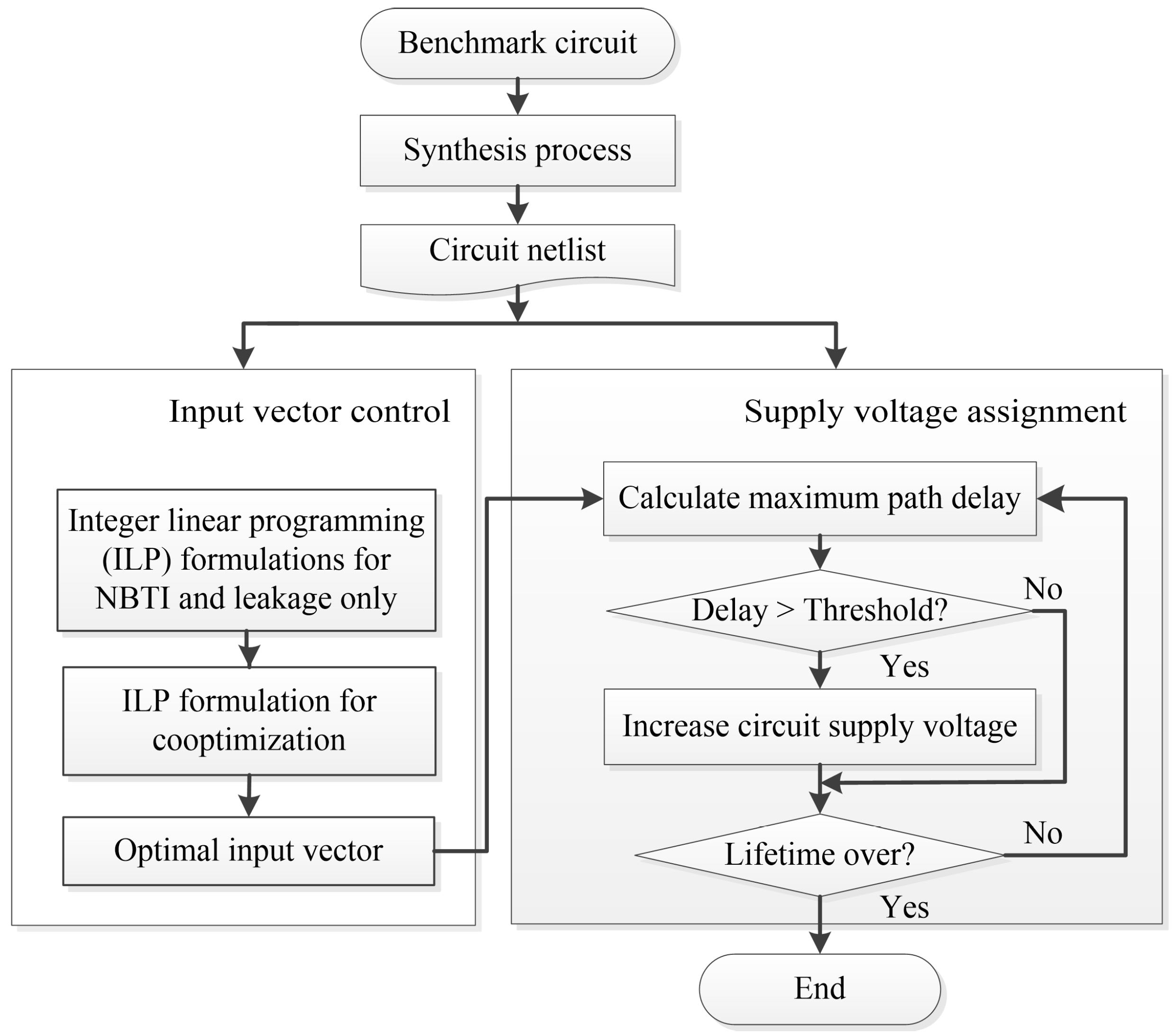
4.2. Result and Discusion

First, we compare the NBTI and leakage reduction results of different IVC methods. We define Pleak and Pdyn as the average leakage power and average dynamic power during the overall lifetime of the circuit, respectively. In the first step, three kinds of ILP formulations are constructed and their corresponding optimal input vectors are found. Then, the corresponding delay degradation ΔD and leakage power Pleak for these input vectors in ten years is calculated, and the result is shown in Table 4.
The delay degradation ΔD that corresponds to the input vector obtained by the IVC #1, IVC #2, and IVC #3 methods is shown in column two to four, respectively. The corresponding leakage power Pleak of these three IVC methods is shown in column five to seven, respectively. From Table 4, we can obtain the following conclusions: first, IVC #1 and IVC #2 can find the optimal ΔD or Pleak minimization result, respectively. However, because only one issue is considered in generating the co-optimization ILP formulation, the reduction result for the other issue is not satisfactory. The proposed ILP formulation considers both effects, and can reduce ΔD and Pleak at the same time. For instance, compared with IVC #1, our proposed IVC #3 method can achieve a 13.15% improvement in Pleak reduction at the cost of a 0.69% ΔD increase on average. On the other hand, compared with IVC #2, our proposed method can decrease ΔD by 8.32% on average, at the cost of a 2.01% increase in leakage power.
As shown in Table 4, the results of the three ILP formulations are different tradeoffs between NBTI and leakage. In the following section, we combine these different IVC methods with the supply voltage assignment, which is a subsequent method after the input vector is determined. In most modern systems, the devices will periodically switch between the active and standby mode, and the circuit’s delay degradation is dependent on the ratio between the active and standby modes (RAS) according to Equations (1)–(6). In some industrial applications, the circuit works under a predefined routine, and the RAS is a fixed value during its lifetime. However, the RAS value in some other applications will change randomly. In order to simplify the experimental setting, we assume that the RAS is fixed, and analyze the NBTI and power reduction results of the combination method when RAS is set to different values. In our future work, we will further analyze the results of our proposed method when the RAS changes randomly.
First, we use three kinds of ILP formulation IVC #1, IVC #2, and IVC #3 to determine the input vector that satisfies the NBTI minimization, leakage minimization, and co-optimization requirements, respectively. Then, the input vector is used in standby mode and the ratio between the active mode and the standby mode is assumed to be 0.1. Afterwards, an SVA method that uses the input vector obtained by IVC #1, IVC #2, and IVC #3, respectively, is applied to compensate for the NBTI-induced performance degradation. The Vdd update cycle for the SVA method is five days, and the resolution for Vdd adjustment is 20 mV. The above process is repeated until the end of the circuit’s lifetime. Then, the average leakage and dynamic power of the circuit in ten years is calculated. The results are shown in Table 5.
In Table 5, the Pleak of SVA combined with IVC #1, IVC #2, and IVC #3 is shown in column two, four, and six, respectively. The Pdyn of SVA combined with these three IVC methods is shown in column three, five, and seven, respectively. Table 5 illustrates that, first, the Pdyn of the SVA + IVC #1 method is the lowest because its aging rate is less severe than that for the SVA + IVC #2 and SVA + IVC #3 methods, and the Vdd increase is the slowest. However, for most circuits, the Pleak of SVA is the highest when the input vector found by IVC #1 is used. This is because the Pleak that corresponds to the input vector obtained by IVC #1 is far higher than that corresponding to the other two ILP formulations when the circuit is in the initial state. Although the leakage power increase is the slowest for SVA + IVC #1, its total leakage power is still the highest at the end of the lifetime. Second, the Pdyn of SVA + IVC #2 is the highest because its corresponding input vector will bring in the most severe NBTI-induced aging, and in turn the frequency of Vdd adjustment is the highest. Third, our proposed co-optimization ILP formulation has considered both NBTI and leakage, and it can find the input vectors that help SVA save 13.82% and 2.49% more leakage power on average than IVC #1 and IVC #2, respectively. In addition, because the NBTI-induced delay degradation that corresponds to our proposed ILP formulation is near optimal, its corresponding Pdyn is close to the Pdyn of SVA + IVC #1 and is lower than the Pdyn when the input vector found by IVC #2 is used. Fourth, different from dynamic power, the analysis for the Pleak of the SVA method is a complex process when using different input vectors. For instance, in the c432 circuit, the input vector obtained by IVC #2 can help SVA save more leakage power than the input vector found by IVC #1. In contrast, the situation is the opposite for c7552 circuit. 
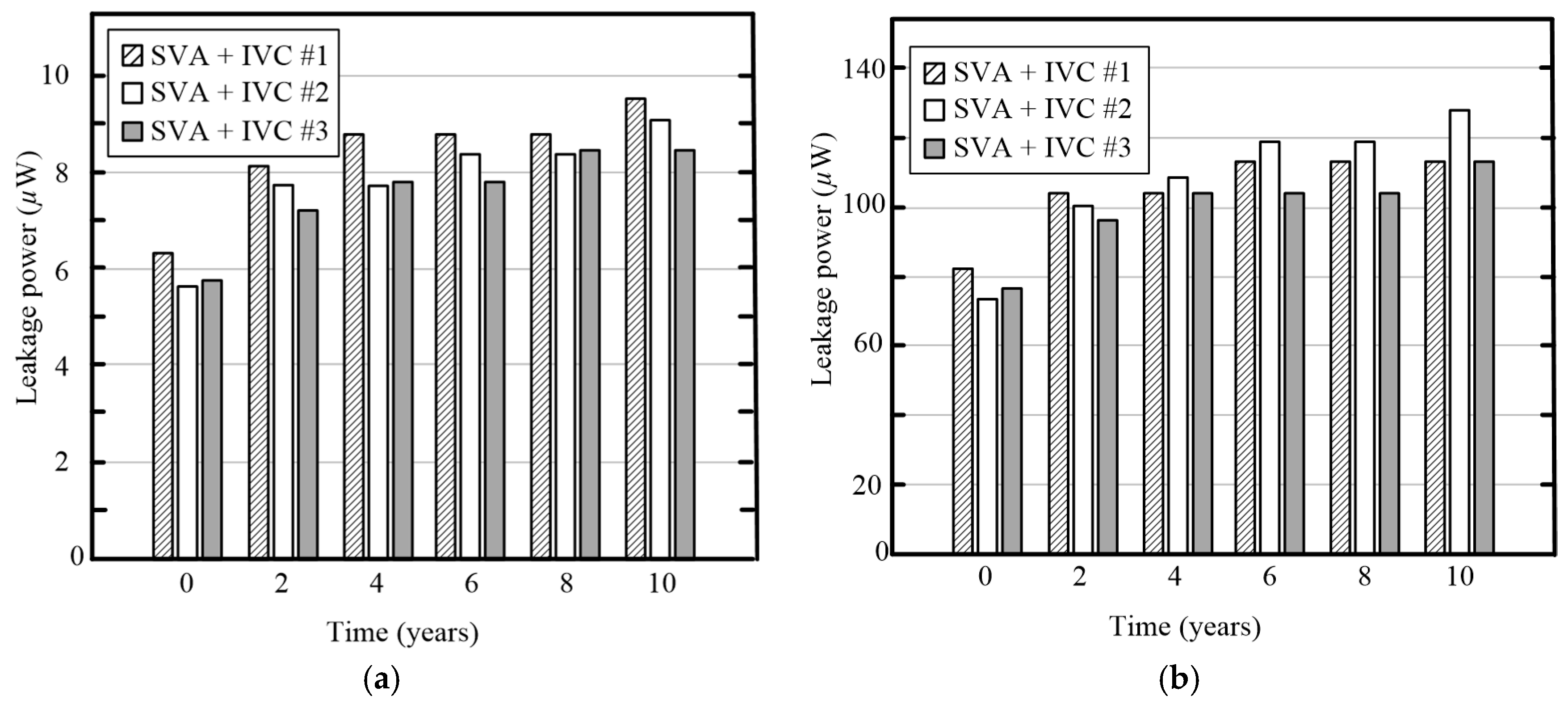
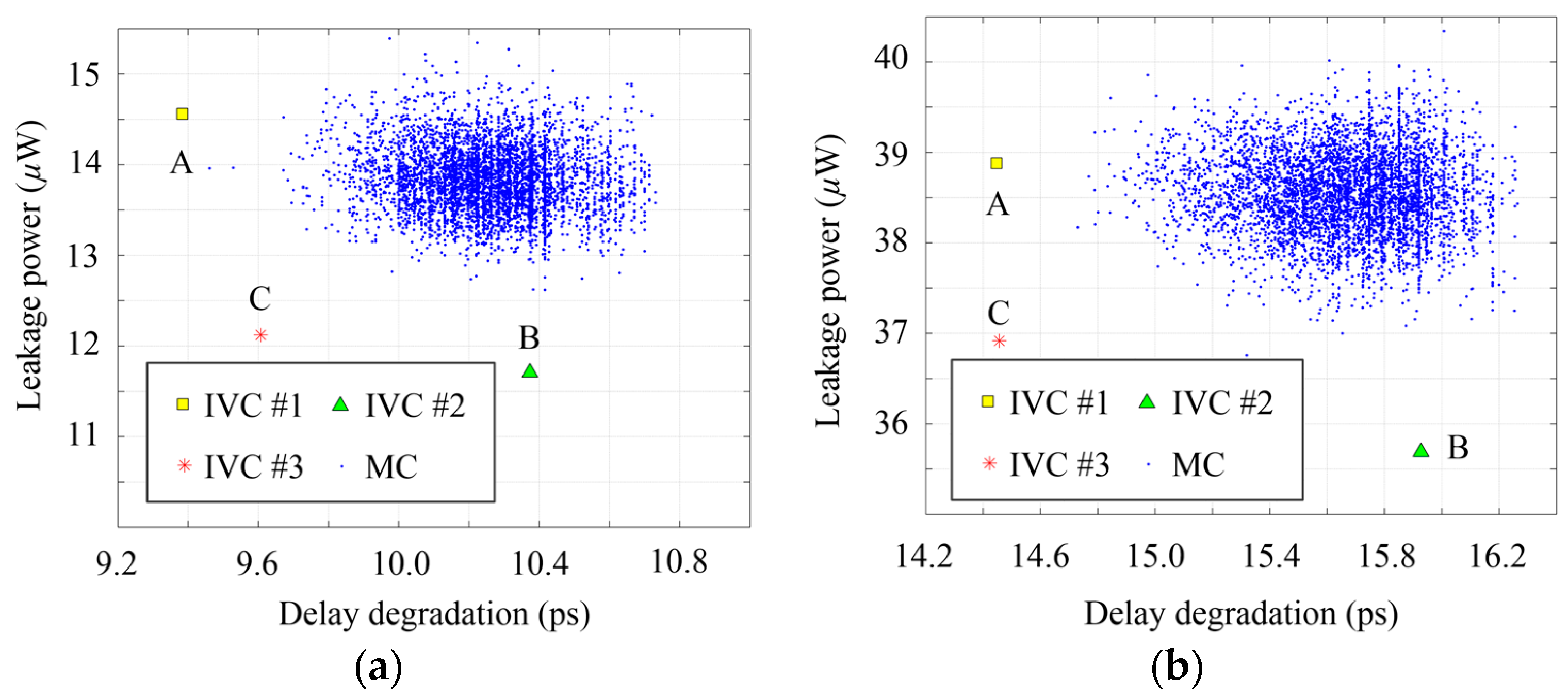
Figure 7 illustrates the change of the leakage power for the c432 and c7552 circuits at each 2-year time interval during the lifetime.
The histograms in Figure 7 show that, for both circuits, the Pleak of SVA + IVC #2 and SVA + IVC #3 increase faster than that of SVA + IVC #1. However, for the c432 circuit, the leakage power in standby mode that corresponds to IVC #1 is much higher than that corresponding to the other two ILP formulations at the starting time (0 year), which makes it still the highest after some iterations of Vdd adjustment. Therefore, the Pleak of SVA + IVC #1 is higher than that of SVA combined with IVC #2 and IVC #3, as shown in Table 5. In contrast, although the initial leakage power that corresponds to the input vector found by IVC #2 is also the lowest for the c7552 circuit, the Pleak of SVA + IVC #2 is the highest for the c7552 circuit. The reason for this phenomenon is that the frequency of Vdd adjustment for SVA + IVC #2 is much faster than for SVA + IVC #1 and IVC #3 because of the severe delay degradation in standby mode, and makes its corresponding leakage power also increase fast as shown in Figure 7b. Finally, we can see that the input vector obtained by our proposed co-optimization ILP formulation can provide a balanced tradeoff between NBTI and leakage, so that both specifications are near optimal, and it can help the SVA save more leakage power than the ILP formulation for a single effect.
Moreover, we have analyzed the power dissipation of the SVA method when RAS is 0.01 and 1.0, and the results are shown in Table 6 and Table 7, respectively.
Table 5, Table 6 and Table 7 show that the power reduction result of the SVA method is dependent on both the input vector in standby mode and the RAS value. First, compared with the SVA + IVC #1 method, our proposed SVA + IVC #3 method can save more leakage power, at the cost of a small increase of dynamic power. Second, when RAS decreases, the advantage of our proposed SVA + IVC #3 method over the SVA + IVC #2 method on power reduction becomes high. For example, when RAS is 0.01, the SVA + IVC #3 method can save 4.28% more leakage power on average than that of SVA + IVC #2. However, when the RAS is 1.0, our proposed method can only save 0.03% more leakage power. The reason for this phenomenon is that when the RAS is small, the ratio of standby mode in the whole lifetime becomes high; the advantage of the input vector found by IVC #1 and IVC #3 on NBTI mitigation becomes more distinct over the input vector obtained by IVC #2. Therefore, the frequency of Vdd adjustment for the SVA method when using the input vector found by IVC #3 is much slower than that of IVC #2, which in turn helps the SVA + IVC #3 method save more leakage and dynamic power than that of the SVA + IVC #2 method.
In Ref. [27], Firouzi et al. have proposed a kind of co-optimization method for NBTI and leakage reduction. This co-optimization ILP formulation is named IVC #4 in the following section. Their method constructed an ILP formulation to find the minimum NBTI-induced delay degradation with different power constraints. In this paper, we also use IVC #4 to find the input vector and analyze the power reduction result of the SVA method when using these input vectors. First, the ILP formulation for leakage minimization and the modified version of ILP formulation for leakage maximization are generated as per the design flow in Ref. [27]. Then, we find the potential best and worst leakage power for the circuit by solving these formulations. Second, a set of power constrains can be built with 10% steps of the leakage power compared to the potential minimum value. With each constrain, an ILP formulation for NBTI mitigation is generated, and the result of these ILP formulations are input vectors, which can obtain the minimum NBTI-induced aging and satisfy the leakage power constrain. Finally, we use each of these ten input vectors in standby mode and apply an SVA to compensate for the performance aging. At the end of the circuit’s lifetime, we calculate the average leakage and dynamic power of an SVA when using each input vector. Suppose Pleak,i and Pdyn,i is the leakage and dynamic power of an SVA corresponding to input vector i. Pleak,min and Pdyn,min is the potential minimum leakage and dynamic power for all of the ten input vectors. Then we define Ei = Pleak,i/Pleak,min + Pdyn,i/Pdyn,min for each input vector i, and the minimum Ei is considered as the optimal result on power reduction for each circuit when using IVC #4. The leakage and dynamic power of the SVA method when using the input vector found by IVC #4 and our proposed IVC #3 method is shown in Table 8.
From Table 8, we can see that compared with the IVC #4 method, our proposed method can save more leakage power dissipation during a circuit’s lifetime, at the cost of a slight increase in dynamic power. Moreover, the design procedure of our proposed method is much simpler than that in Ref. [27], which demonstrates the advantage of our method.
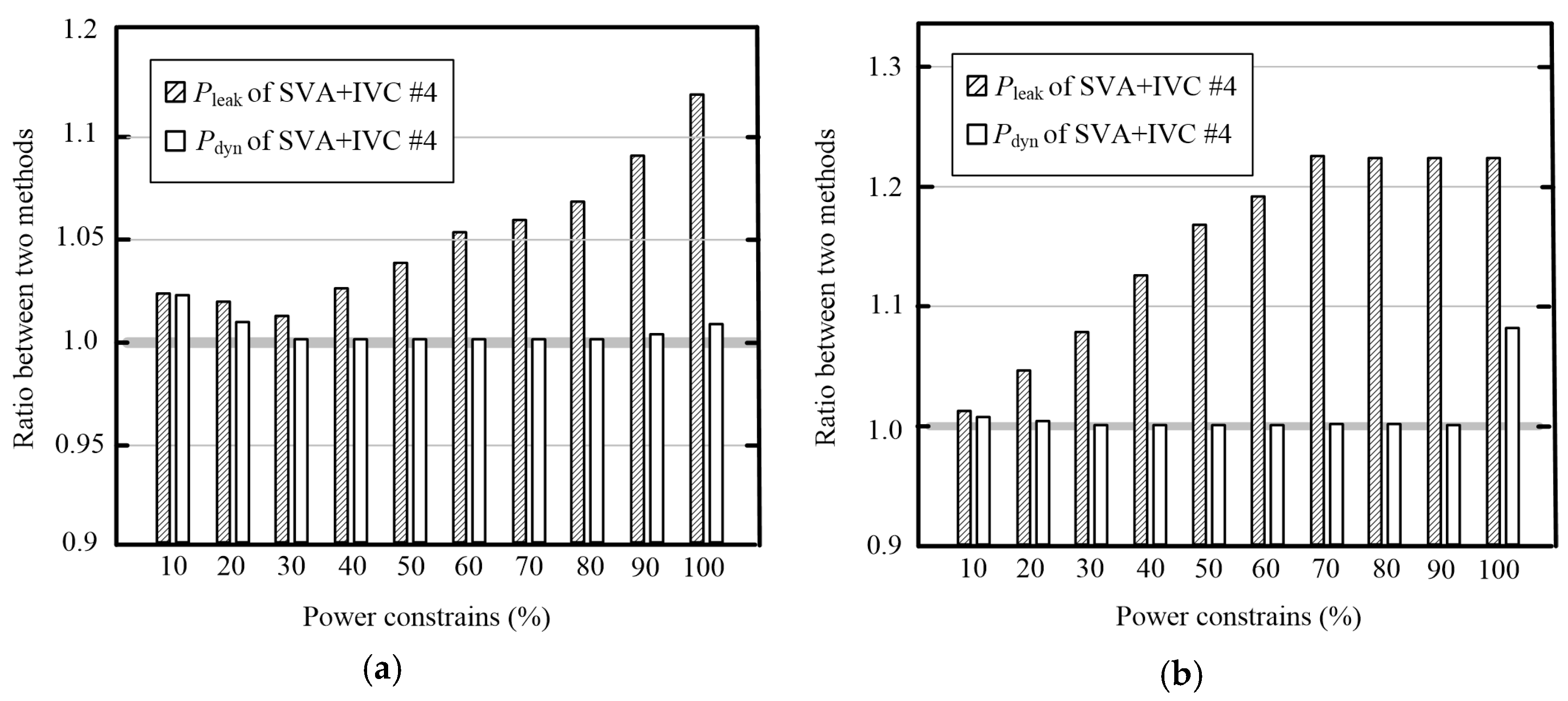
In addition, we implement a simulation on c880 and c3540 circuits to investigate the leakage and dynamic power change of the SVA method when using the input vector obtained by IVC #4 under different power constrains in detail. In order to observe the change more precisely, the leakage and dynamic power results of SVA + IVC #4 are normalized to the power results obtained by the proposed SVA + IVC #3 method. The results are shown in Figure 8.
In Figure 8, the x-axis represents the different power constrains for the ILP formulation in Ref. [27], and the y-axis is the ratio of Pdyn and Pleak between the SVA + IVC #3 method and the SVA + IVC #4 method. Figure 8 shows that, for the different circuits, the co-optimization ILP formulations with different power constrains can obtain the optimal leakage and dynamic power reduction result. For example, the power reduction result is optimal for an c880 circuit when the constrain is 30%. However, for the c3540 circuit, the optimal result can be obtained when the constrain is set to 10%. Therefore, it is inconvenient to find the best parameter for the co-optimization ILP formulation in Ref. [27]. In comparison, our proposed ILP formulation can obtain the only optimal input vector that can help the SVA method save power dissipation conveniently.
Finally, we implement a 5000 times Monte Carlo simulation to find input vectors for the circuit. We calculate the Pleak and Pdyn of the SVA in ten years when these randomly selected input vectors are used in standby mode. The simulation setting is the same as the above section. We compare the power dissipation of SVA + MC with our proposed SVA + IVC #3 method. The result is shown in Table 9.
Table 9 shows that the proposed IVC #3 method can find the optimal input vector and help the SVA save more leakage power than the input vector obtained by MC simulation. Since the dynamic power is strongly dependent on the circuit’s supply voltage in the active mode, the impact of NBTI-induced Vdd change on power dissipation is great. As shown in Figure 6, the result of NBTI mitigation by MC simulation is close or even better than the result by the proposed IVC #3 method, so the best result of the dynamic power for SVA + MC is close to the dynamic power of the SVA + IVC #3 method. Finally, the Pdyn and Pleak of the SVA method for the c880 and c3540 circuits when using the input vector obtained by MC and the three IVC methods are illustrated in Figure 9, respectively.
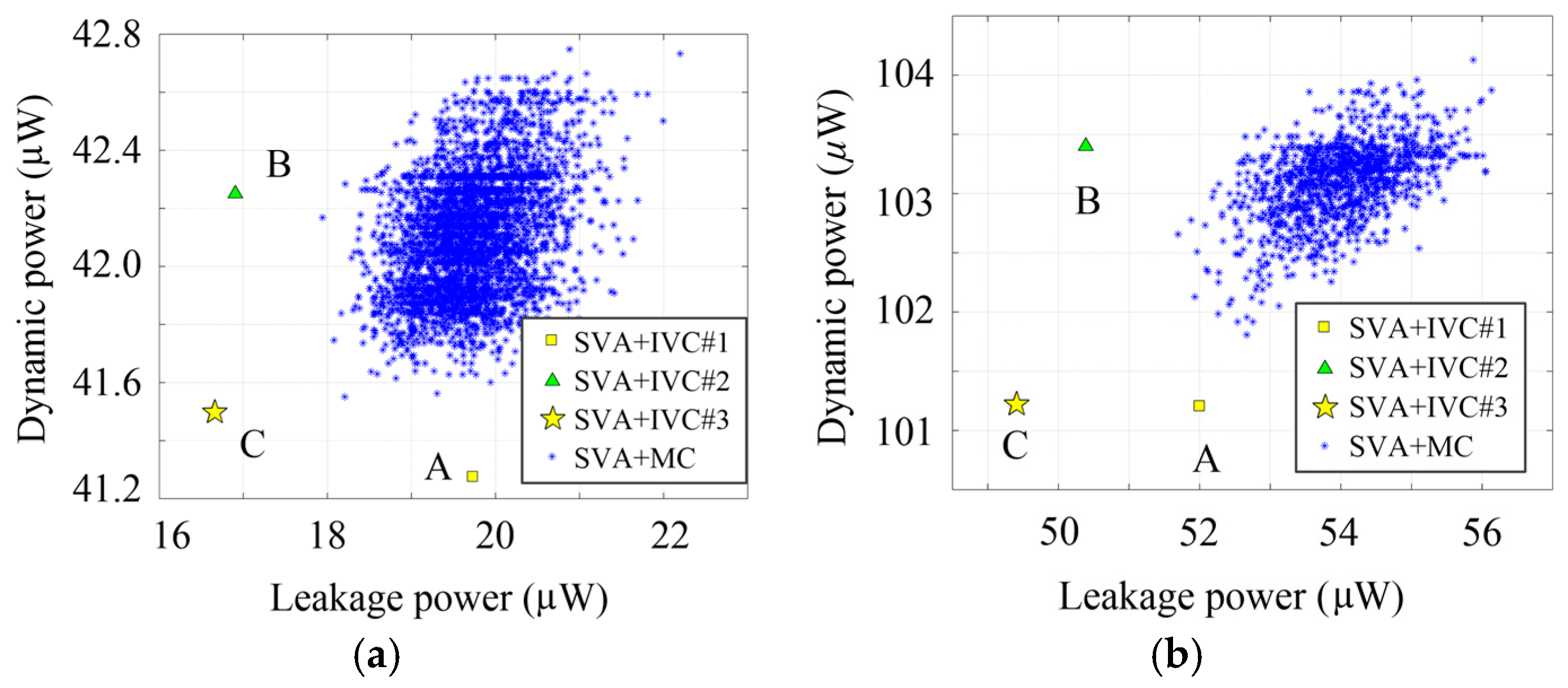
In Figure 9, the x-axis and y-axis represent the leakage and dynamic power of the SVA method, respectively. Point A (the rectangular point) and B (the triangle point) correspond to the result of SVA + IVC #1 and SVA + IVC #2, respectively. Point C (the star point) represents the result of our proposed SVA + IVC #3 method. The small asterisk point represents the leakage and dynamic power of the SVA method using the input vector obtained by MC simulations. The iteration number for MC simulation is 100,000. From Figure 9, we can get the following conclusions: first, the dynamic power of SVA when using the input vector obtained by IVC #1 is the lowest, because the ILP formulation for NBTI reduction can find the minimum degradation vector (MDV), and the frequency of Vdd adjustment for SVA + IVC #1 is the slowest. However, because the initial leakage power that corresponds to IVC #1 is the highest, the total leakage power dissipation for SVA + IVC #1 is the highest among the three ILP formulations. Second, although the leakage power dissipation for SVA + IVC #2 is low, its dynamic power is relatively high because of the high Vdd adjustment frequency. Finally, the Pdyn and Pleak of our proposed SVA + IVC #3 method are all near the optimal result, which demonstrates its advantage over MC simulation and ILP formulations for a single effect.

5. Conclusions

In this paper, an IVC and SVA combination method is proposed to reduce NBTI and leakage simultaneously. First, the dependence of NBTI and leakage on input vectors is analyzed and the procedure for a delay degradation and leakage power reduction technique based on the ILP approach is described. Based on this, a minimum NBTI vector selection method is proposed, which considers the power effect. Our proposed ILP formulation can be generated automatically and the parameters in the objective function can be adjusted adaptively for different circuits, so that the circuit designers can find the optimal input vector conveniently. In addition, we combine our proposed IVC method with the supply voltage assignment technique, and compare the average power dissipation of SVA when using different input vectors in standby mode. The experimental results on ten benchmark circuits show that, compared with MC simulation and the other kinds of ILP formulations, our proposed method can balance the tradeoff between NBTI and leakage, and it can help SVA reduce more power dissipation and guarantee the circuit’s performance simultaneously.

Acknowledgments

This work was supported by the National Natural Science Foundation of China (Nos. 61201015, 61102036, 61571161).

Author Contributions

Peng Sun conceived and designed the experiments; Yang Yu performed the experiments; Junbao Li analyzed the data; and Peng Sun, Zhiming Yang, and Xiyuan Peng wrote the paper. This work was supported by the National Natural Science Foundation of China (Nos. 61201015, 61102036, 61571161).

Conflicts of Interest

The authors declare no conflict of interest.

References

  1. Stathis, J.H.; Zafar, S. The negative bias temperature instability in MOS devices: A review. Microelectron. Reliab. 2006, 46, 270–286. [Google Scholar] [CrossRef]
  2. Wang, Y.; Luo, H.; He, K.; Luo, R.; Yang, H.; Xie, Y. Temperature-aware NBTI modeling and the impact of standby leakage reduction techniques on circuit performance degradation. IEEE Trans. Dependable Secur. Comput. 2011, 8, 756–769. [Google Scholar] [CrossRef]
  3. Roy, K.; Mukhopadhyay, S.; Mahmoodi-Meimand, H. Leakage current mechanisms and leakage reduction techniques in deep-submicrometer CMOS circuits. Proc. IEEE 2003, 91, 305–327. [Google Scholar] [CrossRef]
  4. Haihua, S.; Liu, F.; Devgan, A.; Acar, E.; Nassif, S. Full chip leakage-estimation considering power supply and temperature variations. In Proceedings of the 2003 International Symposium on Low Power Electronics and Design, ISLPED’03, Seoul, Korea, 27 August 2003; pp. 78–83. [Google Scholar]
  5. Chen, Y.-T.; Horng, M.-F.; Lo, C.-C.; Chu, S.-C.; Pan, J.-S.; Liao, B.-Y. A transmission power optimization with a minimum node degree for energy-efficient wireless sensor networks with full-reachability. Sensors 2013, 13, 3951–3974. [Google Scholar] [CrossRef] [PubMed]
  6. Calimera, A.; Macii, E.; Poncino, M. NBTI-aware power gating for concurrent leakage and aging optimization. In Proceedings of the 2009 ACM/IEEE International Symposium on Low Power Electronics and Design, San Fancisco, CA, USA, 19–21 August 2009; pp. 127–132. [Google Scholar]
  7. Wang, Y.; Chen, X.; Wang, W.; Cao, Y.; Xie, Y.; Yang, H. Leakage power and circuit aging cooptimization by gate replacement techniques. IEEE Trans. Very Large Scale Integr. Syst. 2011, 19, 615–628. [Google Scholar] [CrossRef]
  8. Bian, S.; Shintani, M.; Wang, Z.; Hiromoto, M.; Chattopadhyay, A.; Sato, T. Runtime NBTI mitigation for processor lifespan extension via selective node control. In Proceedings of the 2016 IEEE 25th Asian Test Symposium (ATS), Hiroshima, Japan, 21–24 November 2016; pp. 234–239. [Google Scholar]
  9. Agarwal, M.; Paul, B.C.; Zhang, M.; Mitra, S. Circuit failure prediction and its application to transistor aging. In Proceedings of the 25th IEEE VLSI Test Symmposium, Berkeley, CA, USA, 6–10 May 2017; pp. 277–286. [Google Scholar]
  10. Chen, X.; Wang, Y.; Cao, Y.; Ma, Y.; Yang, H. Variation-aware supply voltage assignment for simultaneous power and aging optimization. IEEE Trans. Very Large Scale Integr. Syst. 2012, 20, 2143–2147. [Google Scholar] [CrossRef]
  11. Bhardwaj, S.; Wang, W.; Vattikonda, R.; Cao, Y.; Vrudhula, S. Predictive modeling of the NBTI effect for reliable design. In Proceedings of the IEEE Custom Integrated Circuits Conference 2006, San Jose, CA, USA, 10–13 September 2006; pp. 189–192. [Google Scholar]
  12. Yang, Z.; Yu, Y.; Zhang, C.; Peng, X. NBTI-aware adaptive minimum leakage vector selection using a linear programming approach. Integr. VLSI J. 2016, 53, 126–137. [Google Scholar] [CrossRef]
  13. Alkabani, Y.; Massey, T.; Koushanfar, F.; Potkonjak, M. Input vector control for post-silicon leakage current minimization in the presence of manufacturing variability. In Proceedings of the 2008 45th ACM/IEEE Design Automation Conference, Anaheim, CA, USA, 8–13 June 2008; pp. 606–609. [Google Scholar]
  14. Bild, D.R.; Dick, R.P.; Bok, G.E. Static NBTI reduction using internal node control. ACM Trans. Des. Autom. Electron. Syst. 2012, 17, 1–30. [Google Scholar] [CrossRef]
  15. Lin, I.C.; Lin, C.H.; Li, K.H. Leakage and aging optimization using transmission gate-based technique. IEEE Trans. Comput. Aided Des. Integr. Circuits Syst. 2013, 32, 87–99. [Google Scholar] [CrossRef]
  16. Kumar, S.V.; Kim, C.H.; Sapatnekar, S.S. Adaptive techniques for overcoming performance degradation due to aging in CMOS circuits. IEEE Trans. Very Large Scale Integr. Syst. 2011, 19, 603–614. [Google Scholar] [CrossRef]
  17. Lee, Y.; Kim, T. A fine-grained technique of NBTI-aware voltage scaling and body biasing for standard cell based designs. In Proceedings of the 16th Asia and South Pacific Design Automation Conference (ASP-DAC 2011), Yokohama, Japan, 25–28 January 2011; pp. 603–608. [Google Scholar]
  18. Zhang, L.; Dick, R.P. Scheduled voltage scaling for increasing lifetime in the presence of NBTI. In Proceedings of the 2009 Asia and South Pacific Design Automation Conference, Yokohama, Japan, 19–22 January 2009; pp. 492–497. [Google Scholar]
  19. Mintarno, E.; Skaf, J.; Zheng, R.; Velamala, J.B.; Cao, Y.; Boyd, S.; Dutton, R.W.; Mitra, S. Self-tuning for maximized lifetime energy-efficiency in the presence of circuit aging. IEEE Trans. Comput. Aided Des. Integr. Circuits Syst. 2011, 30, 760–773. [Google Scholar] [CrossRef]
  20. Wang, Y.; Li, X.; Qing, J.; Zeng, Y.; Shi, Y.; Guo, A.; Hu, S.; Chen, S.; Zhao, Y. Analytical parameter extraction for NBTI reaction diffusion and trapping/detrapping models. Microelectron. Reliab. 2016, 66, 10–15. [Google Scholar] [CrossRef]
  21. Velamala, J.B.; Sutaria, K.B.; Sato, T.; Cao, Y. Aging statistics based on trapping/detrapping: Silicon evidence, modeling and long-term prediction. In Proceedings of the 2012 IEEE International Reliability Physics Symposium (IRPS), Anaheim, CA, USA, 15–19 April 2012; pp. 2F.2.1–2F.2.5. [Google Scholar]
  22. Grasser, T.; Waltl, M.; Rzepa, G.; Goes, W.; Wimmer, Y.; El-Sayed, A.M.; Shluger, A.L.; Reisinger, H.; Kaczer, B. The permanent component of NBTI revisited: Saturation, degradation-reversal, and annealing. In Proceedings of the 2016 IEEE International Reliability Physics Symposium (IRPS), Pasadena, CA, USA, 17–21 April 2016. [Google Scholar]
  23. Katsetos, A.A. Negative bias temperature instability (NBTI) recovery with bake. Microelectron. Reliab. 2008, 48, 1655–1659. [Google Scholar] [CrossRef]
  24. Mahapatra, S.; Goel, N.; Desai, S.; Gupta, S.; Jose, B.; Mukhopadhyay, S.; Joshi, K.; Jain, A.; Islam, A.E.; Alam, M.A. A comparative study of different physics-based NBTI models. IEEE Trans. Electron. Devices 2013, 60, 901–916. [Google Scholar] [CrossRef]
  25. Kaczer, B.; Grasser, T.; Roussel, P.J.; Franco, J.; Degraeve, R.; Ragnarsson, L.A.; Simoen, E.; Groeseneken, G.; Reisinger, H. Origin of NBTI variability in deeply scaled pfets. In Proceedings of the 2010 IEEE International Reliability Physics Symposium, Anaheim, CA, USA, 2–6 May 2010; pp. 26–32. [Google Scholar]
  26. Zhao, K.; Stathis, J.H.; Linder, B.P.; Cartier, E.; Kerber, A. PBTI under dynamic stress: From a single defect point of view. In Proceedings of the 2011 International Reliability Physics Symposium, Monterey, CA, USA, 10–14 April 2011; pp. 4A.3.1–4A.3.9. [Google Scholar]
  27. Firouzi, F.; Kiamehr, S.; Tahoori, M.B. Power-aware minimum NBTI vector selection using a linear programming approach. IEEE Trans. Comput. Aided Des. Integr. Circuits Syst. 2013, 32, 100–110. [Google Scholar] [CrossRef]
  28. Bowman, K.A.; Austin, B.L.; Eble, J.C.; Xinghai, T.; Meindl, J.D. A physical alpha-power law mosfet model. IEEE J. Solid State Circuits 1999, 34, 1410–1414. [Google Scholar] [CrossRef]
  29. Xu, Q.; Nicolici, N.; Chakrabarty, K. Test wrapper design and optimization under power constraints for embedded cores with multiple clock domains. IEEE Trans. Comput. Aided Des. Integr. Circuits Syst. 2007, 26, 1539–1547. [Google Scholar] [CrossRef]
  30. Yang, M.; Liu, J. A maximum lifetime coverage algorithm based on linear programming. J. Inf. Hiding Multimed. Signal Process. 2014, 5, 295–300. [Google Scholar]
  31. Richards, A.; How, J.P. Aircraft trajectory planning with collision avoidance using mixed integer linear programming. In Proceedings of the 2002 American Control Conference (IEEE Cat. No.CH37301), Anchorage, AK, USA, 8–10 May 2002; Volume 1933, pp. 1936–1941. [Google Scholar]
  32. Gao, F.; Hayes, J.P. Exact and heuristic approaches to input vector control for leakage power reduction. IEEE Trans. Comput. Aided Des. Integr. Circuits Syst. 2006, 25, 2564–2571. [Google Scholar] [CrossRef]
  33. Wang, Y.; Chen, X.; Wang, W.; Balakrishnan, V.; Cao, Y.; Xie, Y.; Yang, H. On the efficacy of input vector control to mitigate NBTI effects and leakage power. In Proceedings of the 2009 10th International Symposium on Quality Electronic Design, San Jose, CA, USA, 16–18 March 2009; pp. 19–26. [Google Scholar]
  34. Yu, C.H.; Lung, C.L.; Ho, Y.L.; Hsu, R.S.; Kwai, D.M.; Chang, S.C. Thermal-aware on-line scheduler for 3-d many-core processor throughput optimization. IEEE Trans. Comput. Aided Des. Integr. Circuits Syst. 2014, 33, 763–773. [Google Scholar] [CrossRef]
Figure 1. The flow of the proposed input vector control (IVC) and supply voltage assignment (SVA) combination method. NBTI, negative bias temperature instability.
Algorithms 10 00094 g001
Figure 2. The input vector combination and corresponding delay increase for an NAND gate.
Algorithms 10 00094 g002
Figure 3. The basic principle of supply voltage assignment.
Algorithms 10 00094 g003
Figure 4. Leakage power change of an NAND gate under different supply voltage.
Algorithms 10 00094 g004
Figure 5. Threshold voltage change for a positive-channel Metal Oxide Semiconductor (pMOS) transistor with different Vgs.
Algorithms 10 00094 g005
Figure 6. Degradation and leakage minimization result by different ILP formulations. (a) c880 circuit; (b) c3540 circuit.
Algorithms 10 00094 g006
Figure 7. Leakage power dissipation of SVA with different input vectors for c432 and c7552 circuits. c432 circuit; (b) c7552 circuit.
Algorithms 10 00094 g007
Figure 8. Leakage and dynamic power of SVA for the c880 and c3540 circuits when using the input vector obtained by the co-optimization method in Ref. [27] under different power constrain settings. (a) c880 circuit; (b) c3540 circuit.
Algorithms 10 00094 g008
Figure 9. Leakage and dynamic power of SVA for c880 and c3540 circuits when using the input vector obtained by MC simulation and our proposed IVC #3 method. (a) c880 circuit; (b) c3540 circuit.
Algorithms 10 00094 g009
Table 1. ILP objective function for delay degradation of logic gates.
GateLogic FunctionObjective Function
INVb = 1 − aΔD = D0b + D1a
NANDc = 1 − (ab)ΔD = (2D00 + D11D01D10) + (D10D01)a + (D01D00)b − (D00 + D11D01D10)c
NORc = 1 − (ab)ΔD = (D01 + D10D11) + (D11D01)a + (D11D10)b − (D01 + D10D00D11)c
Table 2. ILP compatible logic constrains for basic gates [27].
GateLogic Constrains
INVa + b = 1
NANDc ≤ 2 − ab; c ≥ 1 − a; c ≥ 1 − b
NORc ≥ 1 − ab; c ≤ 1 − a; c ≤ 1 − b
Table 3. ILP objective function for leakage power of logic gates.
GateObjective Function
INVP = P0b + P1a
NANDP = (2P00 + P11P01P10) + (P10P01)a + (P01P00)b − (P00 + P11P01P10)c
NORP = (P01 + P10P11) + (P11P01)a + (P11P10)b − (P01 + P10P00P11)c
Table 4. NBTI and leakage reduction results using different kinds of ILP formulations.
CircuitΔD (ps)Pleak (µW)
IVC #1IVC #2IVC #3IVC #1IVC #2IVC #3
c43210.6811.8510.86.245.695.90
c8809.3810.379.614.5611.7112.12
c190812.3313.1112.4517.6515.7215.95
c26708.488.818.4827.222.9523.28
c354014.4515.9314.4738.8835.6936.92
c531513.6514.7213.7864.0455.2955.7
c755216.7721.2716.9381.8672.4875.44
s53786.26.556.2247.2440.5041.17
s92348.018.158.0164.9757.3257.34
s13,20712.0112.8312.03100.8482.6683.19
Avg.−0.69%8.32% 13.15%−2.01%
Table 5. Leakage and dynamic power of SVA combined with different ILP formulations (RAS = 0.1).
CircuitSVA + IVC #1 (µW)SVA + IVC #2 (µW)SVA + IVC #3 (µW)
PleakPdynPleakPdynPleakPdyn
c4329.2417.868.0618.287.9517.90
c88019.7341.2816.9142.2616.6741.51
c190823.8049.3921.8250.0321.6149.51
c267036.1077.7831.3478.6330.9877.78
c354051.99101.2150.39103.449.39101.23
c531586.02195.0877.18198.4675.08195.59
c7552108.11278.26110.46294.95100.16278.71
s537863.53117.3256.18118.9455.46117.43
s923489.62152.2679.78154.4878.22153.20
s13,207138.88204.41117.46207.18115.67204.49
Avg.13.82%−0.22%2.49%1.89%
Table 6. Leakage and dynamic power of SVA combined with different ILP formulations (RAS = 0.01).
CircuitSVA + IVC #1 (µW)SVA + IVC #2 (µW)SVA + IVC #3 (µW)
PleakPdynPleakPdynPleakPdyn
c4328.5217.267.6517.897.3817.34
c88017.8739.6115.7041.0015.2639.99
c190821.9647.7720.3848.6319.9247.85
c267033.4275.2929.1676.3028.6775.29
c354047.7397.6147.13100.5945.3397.62
c531578.50187.7171.68192.4168.39188.02
c755297.77266.61104.12287.9890.81267.39
s537858.49113.3752.63115.7651.17113.57
s923482.45147.0574.47150.1472.26148.23
s13,207127.09197.03109.01200.94105.96197.17
Avg.13.54%−0.31%4.28%2.69%
Table 7. Leakage and dynamic power of SVA combined with different ILP formulations (RAS = 1.0).
CircuitSVA + IVC #1 (µW)SVA + IVC #2 (µW)SVA + IVC #3 (µW)
PleakPdynPleakPdynPleakPdyn
c43210.1818.588.5818.778.7018.60
c88022.1143.2518.5043.7918.5843.38
c190826.3351.4623.6451.7023.8251.51
c267040.0681.2034.2081.4834.4381.20
c354057.74105.8254.53106.8955.04105.84
c531596.15204.4584.63206.3583.45204.61
c7552125.18295.82118.91304.07115.96296.16
s537870.15122.1260.67122.7161.12122.16
s923499.57159.1586.57159.9086.01159.45
s13,207153.49213.15128.55215.10127.77213.20
Avg.14.16%−0.10%0.03%0.87%
Table 8. Leakage and dynamic power of SVA method using input vector found by Ref. [27] and the proposed ILP formulation.
CircuitSVA + IVC #4 in Ref. [27]the proposed SVA + IVC #3
Pleak (µW)Pdyn (µW)Pleak (µW)Pdyn (µW)
c4327.9517.907.9517.90
c88016.9141.5116.6741.51
c190821.6549.5121.6149.51
c267031.4977.7830.9877.78
c354049.92101.7349.39101.23
c531576.19195.3875.08195.59
c7552100.21278.69100.16278.71
s537856.17117.3255.46117.43
s923480.48153.2078.22153.20
s13,207117.51204.41115.67204.49
Avg.1.16%0.02%
Table 9. Leakage and dynamic power of SVA using an input vector found by Monte Carlo (MC) simulation and the IVC #3 method.
CircuitSVA + MC (µW)SVA + IVC #3
Pleak (µW)Pdyn (µW)Pleak (µW)Pdyn (µW)
c4328.3717.937.9517.90
c88018.2141.5516.6741.51
c190822.6749.7921.6149.51
c267032.7676.6730.9877.78
c354051.93102.1349.39101.23
c531583.11196.6675.08195.59
c7552102.21273.18100.16278.71
s537858.82115.7455.46117.43
s923487.18153.2378.22153.20
s13207129.53205.18115.67204.49
Avg.7.26%−0.22%

