Abstract
This paper presents the preparation of high-quality vanadium dioxide (VO2) thermochromic thin films with enhanced visible transmittance (Tvis) via radio frequency (RF) sputtering and plasma enhanced chemical vapor deposition (PECVD). VO2 thin films with high Tvis and excellent optical switching efficiency (Eos) were successfully prepared by employing SiO2 as a passivation layer. After SiO2 deposition, the roughness of the films was decreased 2-fold and a denser structure was formed. These morphological changes corresponded to the results of optical characterization including the haze, reflectance and absorption spectra. In spite of SiO2 coating, the phase transition temperature (Tc) of the prepared films was not affected. Compared with pristine VO2, the total layer thickness after SiO2 coating was 160 nm, which is an increase of 80 nm. Despite the thickness change, the VO2 thin films showed a higher Tvis value (λ 650 nm, 58%) compared with the pristine samples (λ 650 nm, 43%). This enhancement of Tvis while maintaining high Eos is meaningful for VO2-based smart window applications.
1. Introduction
For improved design and practicality, the exterior of many buildings has been changed into full-window constructions in recent years [1]. However, such window architecture systems lead to more cooling and heating energy loss in the summer and winter seasons. One of the best ways to solve this problem is vanadium dioxide (VO2) based thermochromic smart windows. VO2 is a well-known material that undergoes a fully reversible metal-insulator phase transition (MIT) at 68 °C accompanied by structural changes from a monoclinic (semiconductor with high IR transparency) to a rutile (metallic form with IR reflection) phase [2,3]. These unique properties make VO2 a promising material for application in energy saving smart windows with solar heat control [4,5,6,7,8]. However, for practical applications, several challenges must be improved: the transition temperature (Tc) is too high to apply on real field; the weak optical contrast in the IR region; the luminous transmittance (Tlum) is less than ~40% for films; the unfavorable color (yellow/brown). Up to now, there have been many efforts to improve the above issues [9,10]. More than anything, low visible transmittance (Tvis) is the most critical drawback of VO2 for applications in glazing systems. The low Tvis originates from strong innerband and interband absorption in the short-wavelength range for both the metallic and semiconductive states [11,12]. To enhance the Tvis, band gap adjustment by doping has been attempted. Zhou et al. reported on the preparation of Mg-doped VO2 nanoparticles via hydrothermal synthesis [13]. By controlling the Mg doping contents, they demonstrated the absorption edge of VO2 particles with a blue-shift from 490 to 440 nm at a Mg content of 3.8 at %, representing a widened optical band gap from 2.0 eV for pure VO2 to 2.4 eV with 3.8 at % doping. Similar research was reported by Chen et al., who fabricated Ti-doped VO2 nanoparticles with successful improvement of Tvis by up to 53% via a hydrothermal process [14]. Zhou et al. reported another approach to improve the Tvis of VO2 thin films by designing VO2 thin films with a periodic porous structure [15]. These periodic porous thermochromic VO2 thin films were fabricated via a colloidal lithography approach and exhibited a high Tvis (81% maximum). However, in spite of the significant enhancement of the Tvis, the optical switching efficiency (Eos) of previously reported VO2 thin films is still lower that of traditional low-emission glass. Moreover, it is difficult to control the stoichiometry of a vanadium-oxygen system using the colloidal lithography approach because organic residues from the colloid might influence the valence of VO2 as well as the phase transformation during the annealing process. VO2-based multi-layered structures such as VO2/ZrO2 double layers [16] and TiO2/VO2/TiO2 triple layers [17] are the most effective solutions to the above problems. These antireflective layers including ZrO2 and TiO2 can protect VO2 from oxidation and provide new functions such as photocatalysis in addition to improving the visible transmittance. However, to date, the reported results on applying an anti-reflective layer have been based on more complex procedures or solution processes for which additional annealing is essential. Thus, the reported VO2 thin films contain low Eos originating from inconsistent stoichiometry due to additional annealing or other procedures [18,19].
In this work, high-quality VO2 thermochromic thin films with significantly enhanced Tvis were prepared by applying a SiO2 layer using plasma enhanced chemical vapor deposition (PECVD). This SiO2 layer deposited by the PECVD method has advantages such as the lack of additional post-annealing processes. Thus, damages from oxidation or reduction, which can influence the crystallinity of VO2, do not occur during SiO2 deposition. In addition, high uniformity and reproducibility underscore the attractiveness of PECVD. This paper also explains how the improvement of Tvis was identified through optical analysis.
2. Materials and Methods
2.1. SiO2/VO2 Thin Film Preparation
VO2 thin films were prepared by RF magnetron sputtering with VO2 ceramic targets (Taewon Scientific, Seoul, Korea, 99.9%, 2 inch). Before deposition, the Eagle XG glass (Corning, New York, NY, USA, 2.5 × 2.5 cm2) used as a substrate was cleaned ultrasonically with hydrochloric acid (1 M) and Ethanol, then was subsequently dried with N2. The vacuum chamber was evacuated to 1.2 × 10⁻⁵ Torr, and Ar gas was introduced with 150 sccm. The RF power, working pressure, and distance of the target to the substrate were maintained at 180 W, 46 mTorr and 40 mm, respectively. The deposition time for all samples was fixed at 15 min. The prepared VOx thin films were crystallized via post-annealing under vacuum conditions (10 mTorr) at a temperature of 575 °C for 4 h with a heating rate of 30 °C/min. The SiO2 layer was deposited by PECVD onto the as prepared VO2 thin films under a working pressure of 200 mTorr. Hexamethyldisilazane (HMDSN) was used as a precursor and a thickness of 80 nm was achieved for the SiO2. More detail procedure and conditions of PECVD is described elsewhere [20].
2.2. Characterizations
The surface morphologies of the films were determined using FE-SEM (JEOL, JSM-7100 F, Tokyo, Japan) and AFM (PARK system, XE-100, Suwon, Korea). Crystallization information for the films was determined using X-ray diffraction (XRD) (Bruker D8 Advance system, Billerica, MA, USA) with Cu Kα radiation (λ = 1.5416 Å). Diffraction patterns were collected for 2θ values between 10° and 80° with a 2° glancing angle, and scanned at a rate of 5°/min. The phases present were identified by comparing the peak intensities and their corresponding 2θ values to various vanadium oxide standards using the software PCPDFWIN ver. 2.1 (JCPDS-ICDD, Philadelphia, PA, USA). Raman spectra were collected with a confocal Raman microscope (Witec, ALPHA 300 M, Ulm, Germany) based on the 532 nm CO2 laser. The optical and thermochromic properties of the films were measured at the temperature range between 20 to 100 °C by using a UV-vis-NIR spectrometer (SHIMADZU, UV-3600, Kyoto, Japan) equipped with handmade heating units including a PID temperature controller. For all samples, the integral visible transmittance (Tlum, 390–830 nm) and solar transmittance (Tsol, 280–2500 nm) was obtained based on the earlier publication [21].
3. Results and Discussion
Figure 1 shows the SEM and AFM images of surface morphologies for the pristine VO2 and SiO2/VO2 thin films. For the pristine VO2, the mean grain size and film thickness were around 150 nm and 80 nm, respectively. Moreover, the clearly formed grain boundary was attributed to the surface roughness value of 11.87 nm. On the other hand, changes in the surface morphology of the films with denser and smoother grain boundaries, including those with 160 nm of total thickness, were observed after SiO2 coating. In addition, an average roughness value of 4.91 nm was obtained, which is a 2-fold decrease compared to pristine VO2. The obtained results suggest that the empty space between the grain boundary of pristine VO2 was filled with SiO2 during the PECVD process.
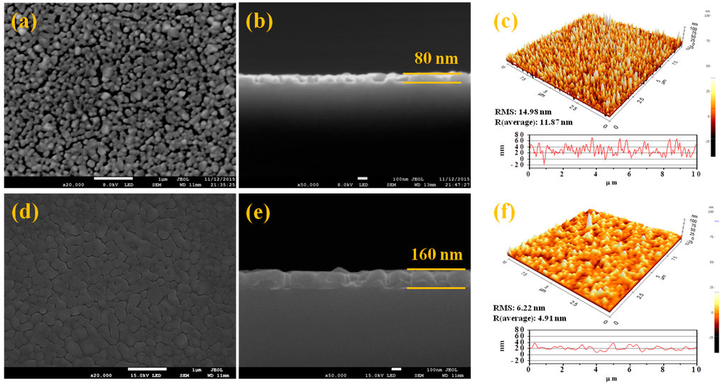
Figure 1.
SEM and AFM images of VO2 (a–c) and SiO2/VO2 (d–f) thin films. The average roughness of the samples was (c): 11.87 nm and (f): 4.91 nm.
Figure 2 shows the XRD data and Raman spectra for each sample. The XRD pattern showed weak signal intensities for the crystallite, resulting from the short-range ordered nanocrystallinity and thinness of the films. The broad shoulder within 15°–40° is due to the contribution of the amorphous SiO2 substrate [22]. A peak at 27.8° that can be ascribed to the (011) plane of monoclinic VO2 (JCPDS no. 82-0661) was observed in the pristine VO2 thin films. For the SiO2/VO2 thin films however, decreased peak intensity was observed, originating from disruption of the thickly covered SiO2 film. Most importantly, no clear diffraction peaks for other vanadium oxides were observed. Raman models corresponding to VO2 (M) appeared in each sample with peaks centered at 135, 192, 225, 263, 308, 338, 392, 440, 499, and 617 cm−1 [23]. The change in Raman shifts for the films was within the measurement accuracy (±2 cm−1). For pristine VO2 thin film, peaks from other types of vanadium oxide were not observed. Moreover, the peaks around 195 cm−1 and 225 cm−1 corresponded to Ag symmetry vibrational modes, which disappeared in VO2 (R) [24,25]. These two vibrational modes play a decisive role in the structural transition of VO2. Thus, the appearance of strong peaks suggests high optical switching characteristics. After SiO2 coating, however, a broad peak around 480 cm−1 attributed to amorphous SiO2 was observed with a moderate signal to noise ratio while the initial peaks corresponding to VO2 (M) remained. In other words, SiO2 coating via PECVD does not affect the crystallinity of VO2 thin films. The corresponding evidence is shown in Figure 3b,c. The hysteresis loop at 2000 nm was obtained from the optical transmittance of each sample as a function of temperature, and a plot of d(Tr)/d(T)&T was obtained from one peak with a well-defined maximum. Each of the d(Tr)/d(T)&T curves were analyzed with a Gaussian function using the single peak fitting module in Origin pro 8.0 software (Originlab, Washington, DC, USA). Distinguishable changes in Tc and hysteresis width, which are closely related to the crystallographic orientation [26], were not observed except for a slight decrease in transmittance.
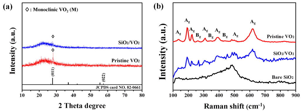
Figure 2.
X-ray diffraction (XRD) (a) and Raman spectra (b) of VO2 and SiO2/VO2 thin films.
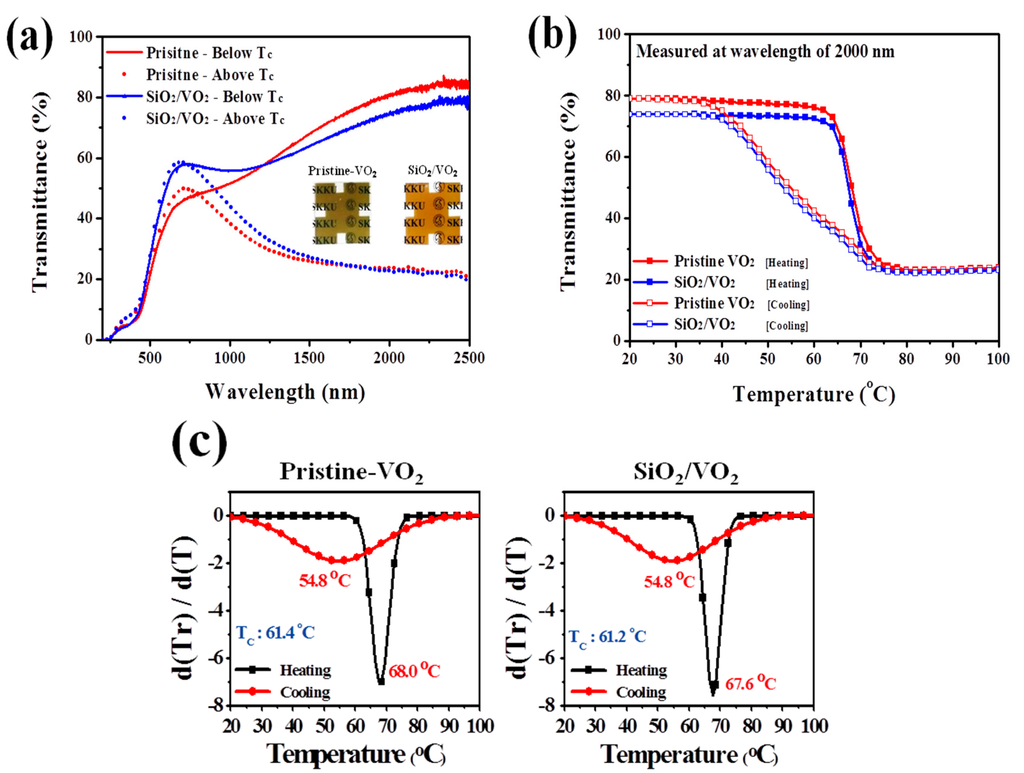
Figure 3.
Transmittance spectra (a); hysteresis loops at 2000 nm (b) as well as corresponding d(Tr)/d(T)&T curve (c) for pristine VO2 and SiO2/VO2 thin films. The inset images in (a) correspond respectively to photographs of the pristine VO2 film (left) and VO2/SiO2 film (right). In (a), solid line measured at 25 °C, dashed line at 100 °C.
The optical analysis results for each sample are shown in Figure 3a. Transmittance results demonstrate the thermochromic properties of each sample measured at 20 °C (solid line) and 100 °C (dashed line). The Eos of the SiO2/VO2 films was 51.7%, which is slightly lower compared with pristine VO2 thin films (57.1%), but the difference is not significant. The SiO2/VO2 thin films showed a significantly enhanced Tvis value (λ650 nm, 58%) compared with the pristine samples (λ650 nm, 43%). In addition, the inset images in Figure 3a clearly show a contrast change after SiO2 coating. Though the SiO2/VO2 film is thicker, it exhibited higher Tvis than the pristine VO2. This enhancement of Tvis can be attributed to two factors. Furthermore, these optical results can be defined by average Tlum((Tlum, 20 °C + Tlum, 100 °C)/2) and ∆Tsol(Tsol, 20 °C − Tsol, 100 °C). The average Tlum of pristine and SiO2/VO2 films are 37.6% and 47.7%, respectively, and ∆Tsol are 8.06 and 7.62. One is the difference in reflectance between pristine VO2 and SiO2/VO2 thin films in the visible region as shown in Figure 4a. As previously mentioned, the formation of smoother and denser grain boundaries after SiO2 coating could reduce the surface roughness, which can influence the decrease of light scattering on the surface observed in SEM images. Therefore, the reflectance for the SiO2/VO2 thin films was decreased from 8% to 4% compared to the pristine VO2 thin films. However, the change in the reflectance is not enough to confirm the enhancement of Tvis for SiO2/VO2 thin films. Figure 4b shows the haze for each sample in the visible region. For the SiO2/VO2 thin films, a slight decrease in haze over 500 nm was observed but other considerable changes did not appear. For this reason, more evidence is needed to validate the transmittance results.
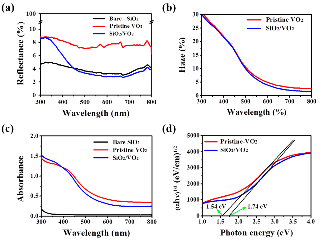
Figure 4.
Optical analysis data for each film based on the reflectance (a); haze (b); absorbance (c) and optical band gap graph (d).
Figure 4c shows the absorbance data for each sample measured in the visible region. The data obviously confirm the change in the absorption edge toward the blue region and a decrease in absorbance after SiO2 coating. The relative optical band gap for each sample is shown in Figure 4d, and the results correspond to the results for reflectance and absorbance. The absorption coefficient α was estimated using the transmittance data for the two films [27].
where ∆d is the thickness of pristine VO2 or SiO2/VO2, T1 is the transmittance of the substrate (Eagle glass) and T2 is the transmittance of each sample. The optical band gap was determined with the following formula [28].
linear extrapolation of (αhν)1/2 vs. hν near the band gap provided Eg as the intercept at the α = 0 axis. The optical band gap for the pristine VO2 thin film increased from 1.54 to 1.74 eV after SiO2 coating. This widening of the optical band gap induces a blue shift and an enhanced visible transmittance [15]. This means that the enhancement of Tvis for SiO2/VO2 corresponds to the decrease in absorbance and reflectance including the formation of denser and smoother surfaces on the films.
α = (1/∆d)ln(T1/T2)
(αhν)1/2 ∝ (E − Eg)
4. Conclusions
In this paper, high-quality VO2 thermochromic thin films with enhanced Tvis up to 58% were successfully prepared with the addition of a SiO2 layer. The results indicate that the enhanced Tvis was due to a reduction of surface roughness with a blue shift in the absorption spectra observed after SiO2 coating. In addition, the SiO2/VO2 thin films had high Eos and the crystallographic orientation was maintained. This enhancement of Tvis while maintaining high Eos is meaningful for VO2-based smart window applications.
Acknowledgments
This work was supported by the Mid-career Researcher Program (2015R1A2A2A01007150) through an National Research Foundation of Korea (NRF) grant funded by the Ministry of Education, Science and Technology (MEST) and the Energy Efficiency & Resources Core Technology Program of the Korea Institute of Energy Technology Evaluation and Planning (KETEP), granted financial resource from the Ministry of Trade, Industry & Energy, Republic of Korea. (No. 20142020104130).
Author Contributions
Sang-Hun Nam and Jin-Hyo Boo proposed the research topic and supervised the entire project. Jung-Hoon Yu designed the experiments, performed the optical characterization and wrote the manuscript. All the authors contributed to the writing and approved the final manuscript.
Conflicts of Interest
The authors declare no conflict of interest.
Abbreviations
The following abbreviations are used in this manuscript:
| PECVD | Plasma enhanced chemical vapor deposition |
| Tvis | Visible transmittance |
| Eos | Optical switching efficiency |
| VO2 | Vanadium dioxide |
| MIT | Metal-insulator transition |
| SEM | Scanning electron microscopy |
| XRD | X-ray diffraction |
References
- Hee, W.J.; Alghoul, M.A.; Bakhtyar, B.; OmKalthum, E.; Shameri, M.A.; Alrubaih, M.S.; Sopian, K. The role of window glazing on daylighting and energy saving in buildings. Renew. Sustain. Energy Rev. 2015, 42, 323–343. [Google Scholar] [CrossRef]
- Morin, F.J. Oxides which show a metal-to-insulator transition at the neel temperature. Phys. Rev. Lett. 1959, 3, 34–36. [Google Scholar] [CrossRef]
- Qazilbash, M.M.; Brehm, M.; Andreev, G.O.; Kim, B.J.; Yun, S.J.; Balatsky, A.V.; Maple, M.B.; Keilmann, F.; Kim, H.T.; Basov, D.N. Mott transition in VO2 revealed by infrared spectroscopy and nano-imaging. Science 2007, 318, 1750–1753. [Google Scholar] [CrossRef] [PubMed]
- Cao, C.; Gao, Y.; Luo, H. Pure single-crystal rutile vanadium dioxide powders: Synthesis, mechanism and phase-transformation property. J. Phys. Chem. C 2008, 112, 18810–18814. [Google Scholar] [CrossRef]
- Kang, L.; Gao, Y.; Luo, H. A Novel solution process for the synthesis of VO2 thin films with excellent thermochromic properties. ACS Appl. Mater. Interfaces 2009, 1, 2211–2218. [Google Scholar] [CrossRef] [PubMed]
- Mlyuka, N.R.; Niklasson, G.A.; Granqvist, C.G. Thermochromic multilayer films of VO2 and TiO2 with enhanced transmittance. Sol. Energy Mater. Sol. Cells 2009, 93, 1685–1687. [Google Scholar] [CrossRef]
- Vernardou, D.; Louloudakis, D.; Spanakis, E.; Katsarakis, N.; Koudoumas, E. Thermochromic amorphous VO2 coatings grown by APCVD using a single-precursor. Sol. Energy Mater. Sol. Cells 2014, 128, 36–40. [Google Scholar] [CrossRef]
- Drosos, C.; Vernardou, D. Perspectives of energy materials grown by APCVD. Sol. Energy Mater. Sol. Cells 2015, 140, 1–8. [Google Scholar] [CrossRef]
- Wang, S.; Liu, M.; Kong, L.; Long, Y.; Jiang, X.; Yu, A. Recent progress in VO2 smart coating: Strategies to improve the thermochromic properties. Prog. Mater. Sci. 2016, 81, 1–54. [Google Scholar] [CrossRef]
- Zhou, Y.; Cai, Y.; Hu, X.; Long, Y. VO2/hydrogel hybrid nanothermochromic material with ultra-high solar modulation and luminous transmission. J. Mater. Chem. A 2015, 3, 1121–1126. [Google Scholar] [CrossRef]
- Burkhardt, W.; Christmann, T.; Franke, S.; Kriegseis, W.; Meister, D.; Meyer, B.K.; Niessner, W.; Schalch, D.; Scharmann, A. Tungsten and fluorine co-doping of VO2 films. Thin Sol. Films 2002, 402, 226–231. [Google Scholar] [CrossRef]
- Qazilbash, M.M.; Schafgans, A.A.; Burch, K.S.; Yun, S.J.; Chae, B.G.; Kim, B.J.; Kim, H.T.; Basov, D.N. Electrodynamics of the vanadium oxides VO2 and V2O3. Phys. Rev. B 2008, 77, 115121. [Google Scholar] [CrossRef]
- Zhou, J.; Gao, Y.; Liu, X.; Chen, Z.; Dai, L.; Cao, C.; Luo, H.; Kanahira, M.; Sunc, C.; Yanc, L. Mg-doped VO2 nanoparticles: Hydrothermal synthesis, enhanced visible transmittance and decreased metal–insulator transition temperature. Phys. Chem. Chem. Phys. 2013, 15, 7505–7511. [Google Scholar] [CrossRef] [PubMed]
- Chen, S.; Dai, L.; Liu, J.; Gao, Y.; Liu, X.; Chen, Z.; Zhou, J.; Cao, C.; Han, P.; Kanahiraa, M. The visible transmittance and solar modulation ability of VO2 flexible foils simultaneously improved by Ti doping: An optimization and first principle study. Phys. Chem. Chem. Phys. 2013, 15, 17537–17543. [Google Scholar] [CrossRef] [PubMed]
- Zhou, M.; Bao, J.; Tao, M.; Zhu, R.; Lin, Y.; Xie, Y. Periodic porous thermochromic VO2(M) films with enhanced visible transmittance. Chem. Commun. 2013, 49, 6021–6023. [Google Scholar] [CrossRef] [PubMed]
- Xu, G.; Jin, P.; Tazawa, M.; Yoshimura, K. Optimization of antireflection coating for VO2-based energy efficient window. Sol. Energy Mater. Sol. Cells 2004, 83, 29–37. [Google Scholar] [CrossRef]
- Jin, P.; Xu, G.; Tazawa, M.; Yoshimura, K. Design, formation and characterization of a novel multifunctional window with VO2 and TiO2 coatings. Appl. Phys. A 2003, 77, 455–459. [Google Scholar]
- Kusano, E.; Theil, J.A. Effects of microstructure and nonstoichiometry on electrical properties of vanadium dioxide films. J. Vac. Sci. Technol. A 1989, 7, 1314–1317. [Google Scholar] [CrossRef]
- Griffiths, C.H.; Eastwood, H.K. Influence of stoichiometry on the metal-semiconductor transition in vanadium dioxide. J. Appl. Phys. 1974, 45, 2201–2206. [Google Scholar] [CrossRef]
- Jin, S.B.; Lee, J.S.; Choi, Y.S.; Choi, I.S.; Han, J.G. High-rate deposition and mechanical properties of SiOx film at low temperature by plasma enhanced chemical vapor deposition with the dual frequencies ultra high frequency and high frequency. Thin Sol. Films 2011, 519, 6334–6338. [Google Scholar] [CrossRef]
- Wang, N.; Liu, S.; Zeng, X.T.; Magdassi, S.; Long, Y. Mg/W-codoped vanadium dioxide thin films with enhanced visible transmittance and low phase transition temperature. J. Mater. Chem. C 2015, 3, 6771–6777. [Google Scholar] [CrossRef]
- Li, J.; Dho, J. Anomalous optical switching and thermal hysteresis behaviors of VO2 films on glass substrate. Appl. Phys. Lett. 2011, 99, 231909. [Google Scholar] [CrossRef]
- Petrov, G.I.; Yakovlev, V.V.; Squier, J. Raman microscopy analysis of phase transformation mechanisms in vanadium dioxide. Appl. Phys. Lett. 2002, 81, 1023–1025. [Google Scholar] [CrossRef]
- Donev, E.U.; Lopez, R.; Feldman, L.C.; Haglund, R.F. Confocal raman microscopy across the metal-insulator transition of single vanadium dioxide nanoparticles. Nano Lett. 2009, 9, 702–106. [Google Scholar] [CrossRef] [PubMed]
- Vernardou, D.; Louloudakis, D.; Spanakis, E.; Katsarakis, N.; Koudoumas, E. Functional Properties of APCVD VO2 Layers. Int. J. Thin Films Sci. Technol. 2015, 4, 187–191. [Google Scholar]
- Du, J.; Gao, Y.; Luo, H.; Kang, L.; Zhang, Z.; Chen, Z.; Cao, C. Significant changes in phase-transition hysteresis for Ti-doped VO2 films prepared by polymer-assisted deposition. Sol. Energy Mater. Sol. Cells 2010, 95, 469–475. [Google Scholar] [CrossRef]
- Kim, E.; Jiang, Z.; No, K. Measurement and calculation of optical band gap of chromium aluminum oxide films. Jpn. J. Appl. Phys. 2000, 39, 4820–4825. [Google Scholar] [CrossRef]
- Jiang, M.; Li, Y.; Li, S.; Zhou, H.; Cao, X.; Bao, S.; Gao, Y.; Luo, H.; Jin, P. Room temperature optical constants and band gap evolution of phase pure M1-VO2 thin films deposited at different oxygen partial pressures by reactive magnetron sputtering. J. Nanomater. 2014, 2014, 183954. [Google Scholar] [CrossRef]
© 2016 by the authors; licensee MDPI, Basel, Switzerland. This article is an open access article distributed under the terms and conditions of the Creative Commons Attribution (CC-BY) license (http://creativecommons.org/licenses/by/4.0/).