
Influence of Oxygen Partial Pressure during Processing on the Thermoelectric Properties of Aerosol-Deposited CuFeO2

Abstract
:1. Introduction
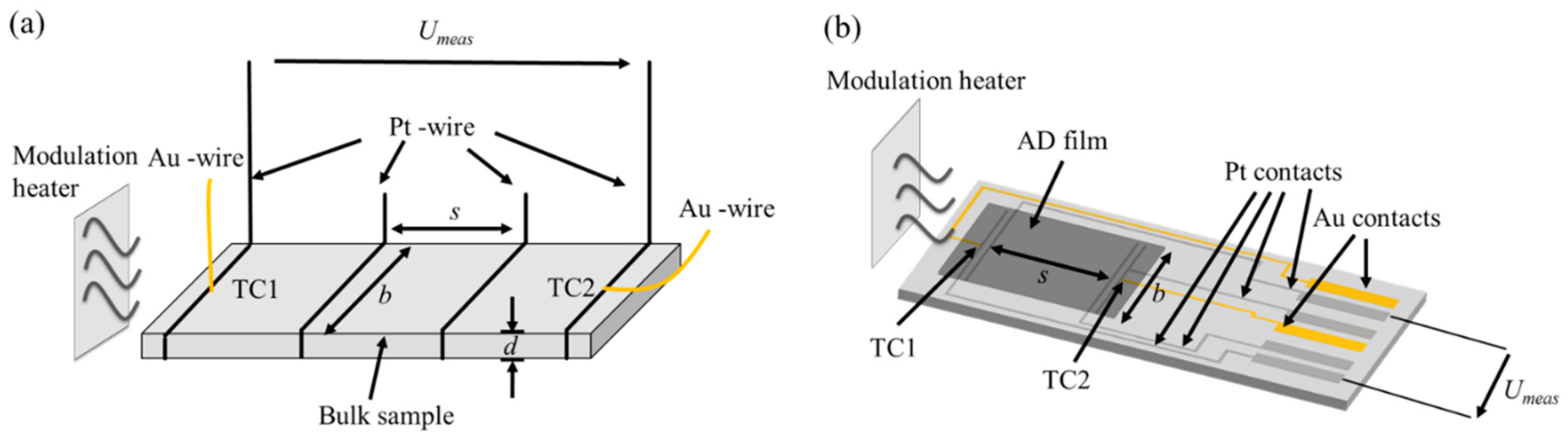
2. Experimental
3. Results and Discussion
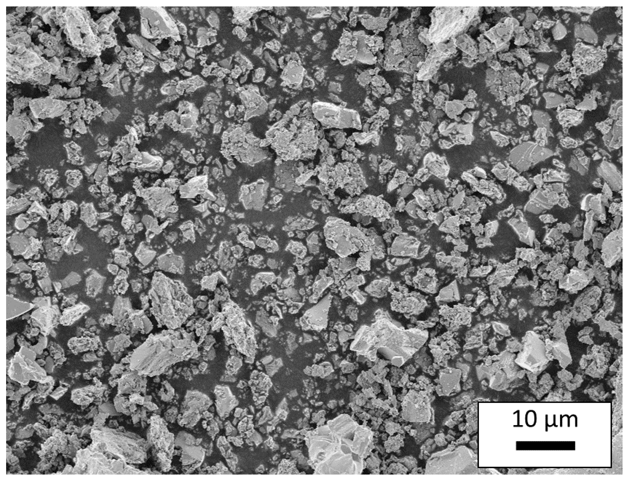
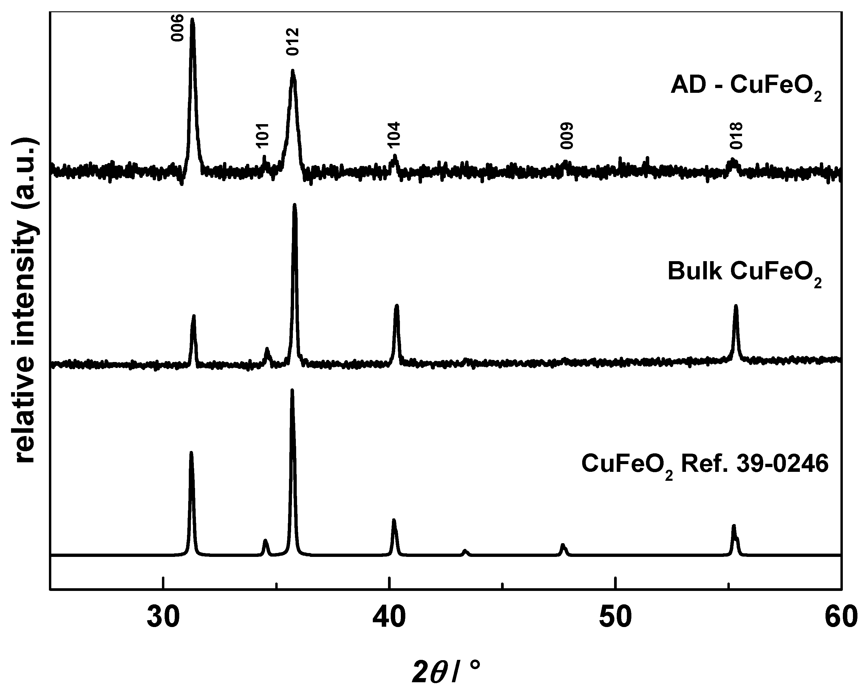
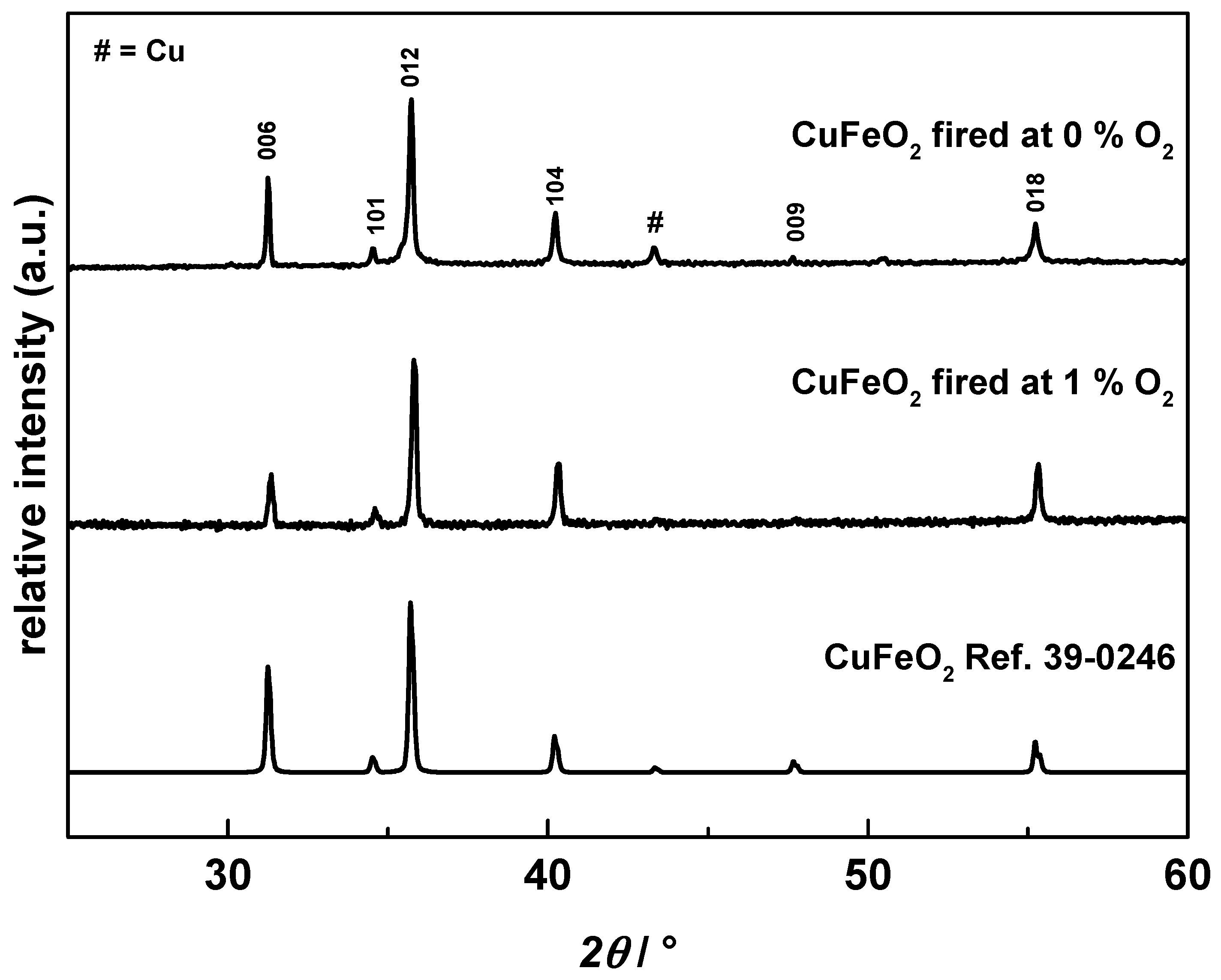
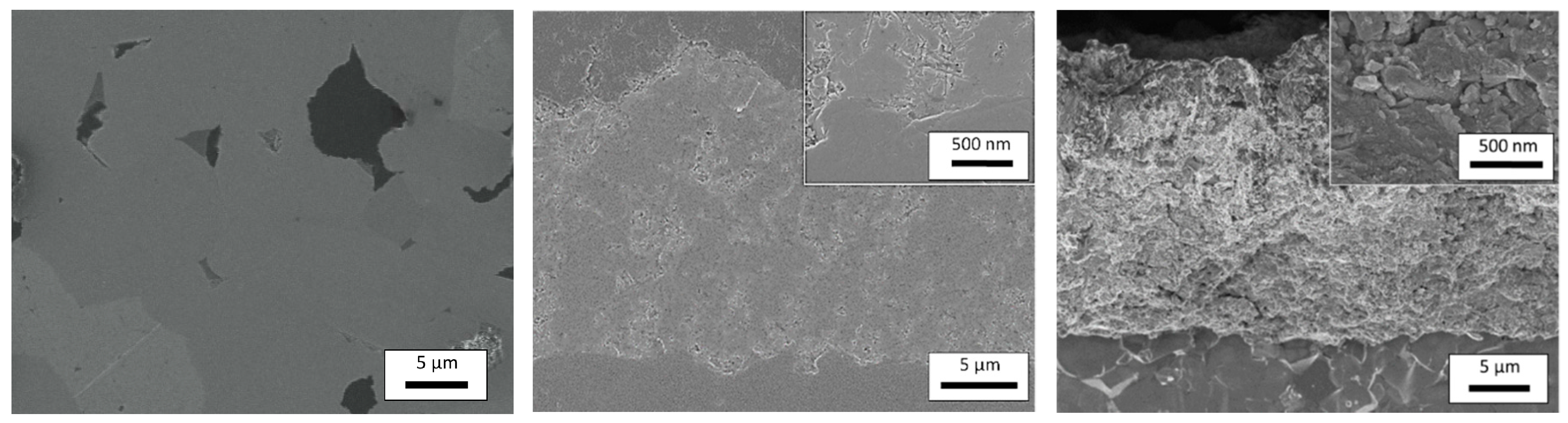
3.1. Characterization of the Synthesized CuFeO2 Powders and AD Films
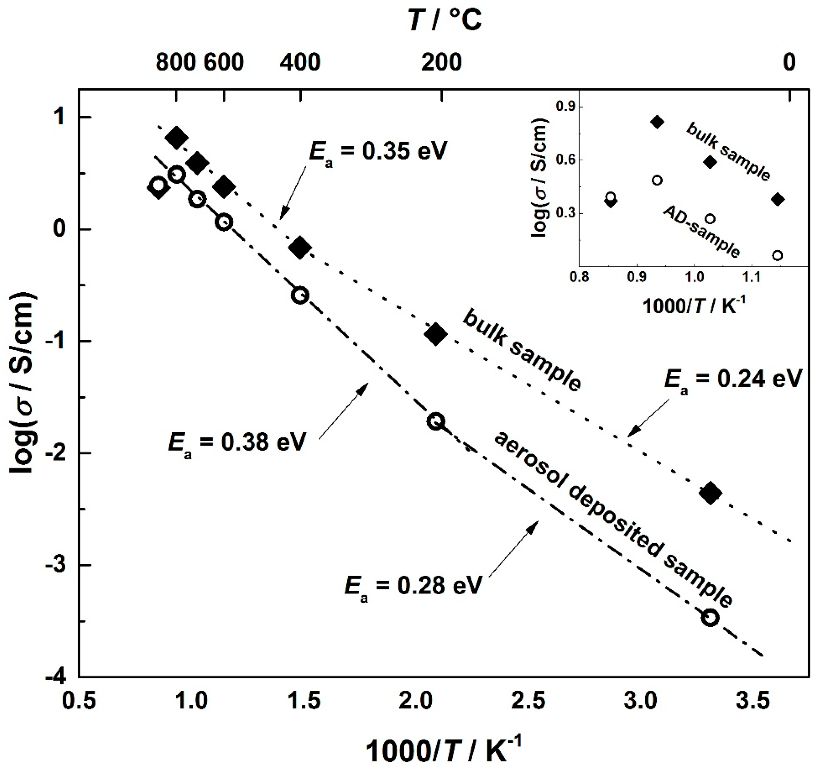
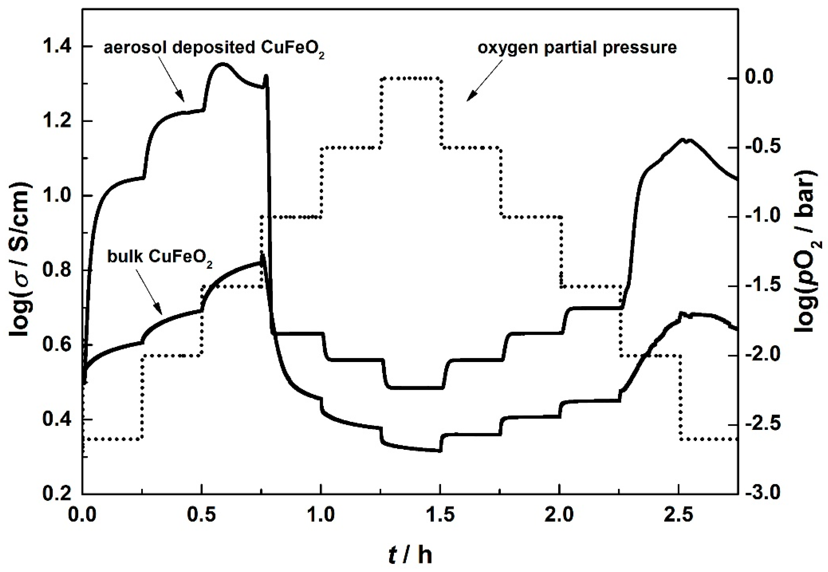
3.2. Electrical Conductivity of Aerosol-Deposited and Bulk CuFeO2
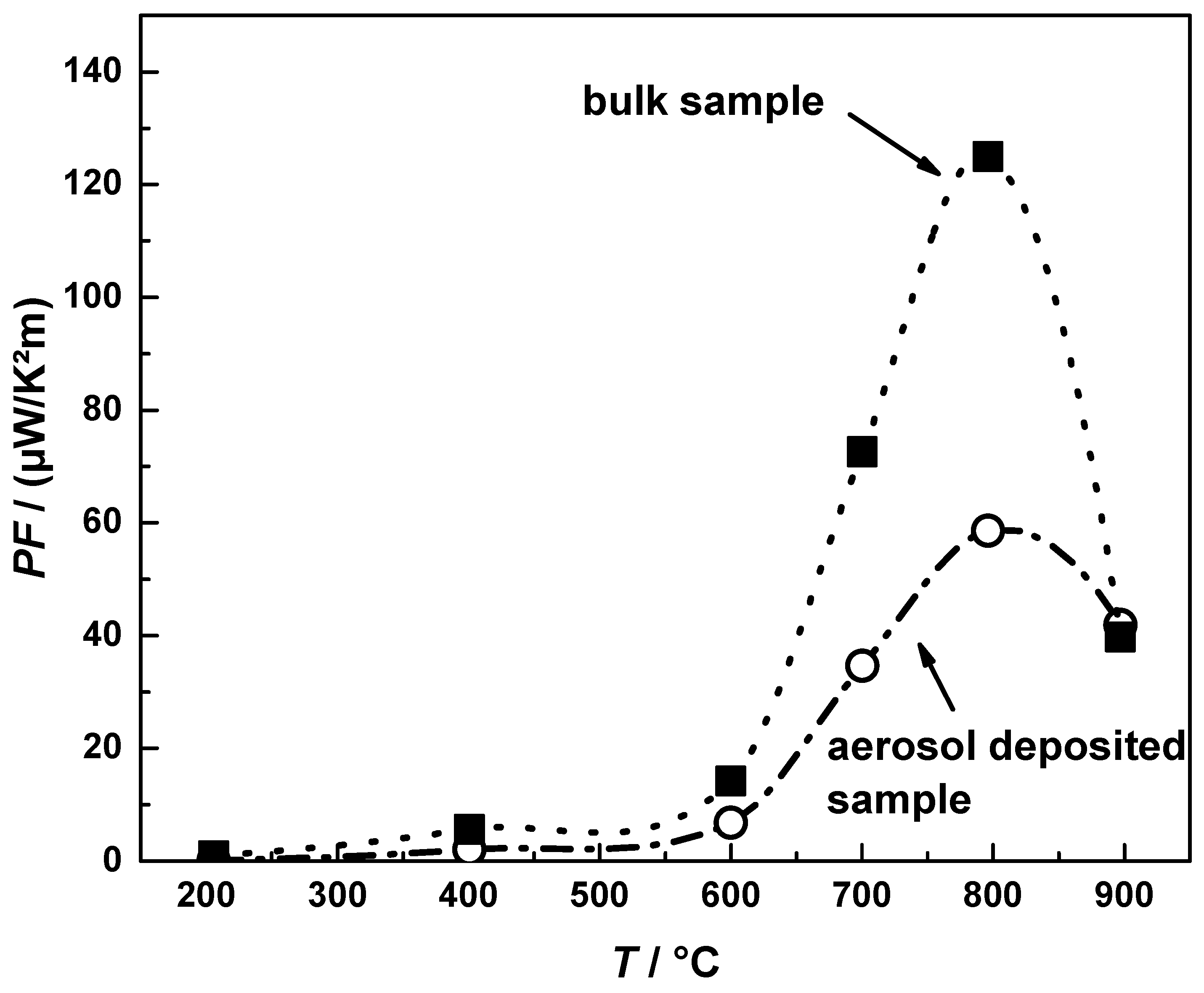
3.3. Thermoelectric Properties of Aerosol Deposited and Bulk CuFeO2
4. Conclusions
Acknowledgments
Author Contributions
Conflicts of Interest
References
- He, J.; Kanatzidis, M.G.; Dravid, V.P. High performance bulk thermoelectrics via a panoscopic approach. Mater. Today 2013, 16, 166–176. [Google Scholar] [CrossRef]
- Snyder, G.J.; Toberer, E.S. Complex thermoelectric materials. Nat. Mater. 2008, 7, 105–114. [Google Scholar] [CrossRef] [PubMed]
- Rowe, D.M. CRC Handbook of Thermoelectrics; CRC Press: Boca Raton, FL, USA, 1995. [Google Scholar]
- Nolas, G.S.; Sharp, J.; Goldsmid, H.J. Thermoelectrics: Basic Principles and New Materials Developments; Springer: Berlin, Germany, 2001. [Google Scholar]
- Rowe, D.M. Thermoelectrics Handbook: Macro to Nano; CRC Taylor & Francis: Boca Raton, FL, USA, 2006. [Google Scholar]
- Sootsman, J.R.; Chung, D.Y.; Kanatzidis, M.G. Alte und neue Konzepte für thermoelektrische Materialien. Angew. Chem. 2009, 121, 8768–8792. [Google Scholar] [CrossRef]
- Zhao, L.-D.; Lo, S.-H.; Zhang, Y.; Sun, H.; Tan, G.; Uher, C.; Wolverton, C.; Dravid, V.P.; Kanatzidis, M.G. Ultralow thermal conductivity and high thermoelectric figure of merit in SnSe crystals. Nature 2014, 508, 373–377. [Google Scholar] [CrossRef] [PubMed]
- Chen, G.; Dresselhaus, M.S.; Dresselhaus, G.; Fleurial, J.-P.; Caillat, T. Recent developments in thermoelectric materials. Int. Mater. Rev. 2003, 48, 45–66. [Google Scholar] [CrossRef]
- Vineis, C.J.; Shakouri, A.; Majumdar, A.; Kanatzidis, M.G. Nanostructured thermoelectrics: Big efficiency gains from small features. Adv. Mater. 2010, 22, 3970–3980. [Google Scholar] [CrossRef] [PubMed]
- Dresselhaus, M.S.; Chen, G.; Tang, M.Y.; Yang, R.G.; Lee, H.; Wang, D.Z.; Ren, Z.F.; Fleurial, J.-P.; Gogna, P. New directions for low-dimensional thermoelectric materials. Adv. Mater. 2007, 19, 1043–1053. [Google Scholar] [CrossRef]
- Poudel, B.; Hao, Q.; Ma, Y.; Lan, Y.; Minnich, A.; Yu, B.; Yan, X.; Wang, D.; Muto, A.; Vashaee, D.; et al. High-thermoelectric performance of nanostructured bismuth antimony telluride bulk alloys. Science 2008, 320, 634–638. [Google Scholar] [CrossRef] [PubMed]
- Bubnova, O.; Crispin, X. Towards polymer-based organic thermoelectric generators. Energy Environ. Sci. 2012, 5, 9345–9362. [Google Scholar] [CrossRef]
- Bubnova, O.; Khan, Z.U.; Malti, A.; Braun, S.; Fahlman, M.; Berggren, M.; Crispin, X. Optimization of the thermoelectric figure of merit in the conducting polymer poly(3,4-ethylenedioxythiophene). Nat. Mater. 2011, 10, 429–433. [Google Scholar] [CrossRef] [PubMed]
- Plochmann, B.; Lang, S.; Rüger, R.; Moos, R. Optimization of thermoelectric properties of metal-oxide-based polymer composites. J. Appl. Polym. Sci. 2013, 131, 40038. [Google Scholar] [CrossRef]
- Stöcker, T.; Köhler, A.; Moos, R. Why does the electrical conductivity in PEDOT:PSS decrease with PSS content? A study combining thermoelectric measurements with impedance spectroscopy. J. Polym. Sci. B Polym. Phys. 2012, 50, 976–983. [Google Scholar] [CrossRef]
- He, M.; Qiu, F.; Lin, Z. Towards high-performance polymer-based thermoelectric materials. Energy Environ. Sci. 2013, 6, 1352–1641. [Google Scholar] [CrossRef]
- Kim, G.H.; Shao, L.; Zhang, K.; Pipe, K.P. Engineered doping of organic semiconductors for enhanced thermoelectric efficiency. Nat. Mater. 2013, 12, 719–723. [Google Scholar] [CrossRef] [PubMed]
- Bérardan, D.; Byl, C.; Dragoe, N. Influence of the Preparation conditions on the thermoelectric properties of Al-Doped ZnO. J. Am. Ceram. Soc. 2010, 93, 2352–2358. [Google Scholar] [CrossRef]
- Dragoe, N.; Bérardan, D.; Byl, C. On the high temperature transport properties of thermoelectric oxides. Phys. Status Solidi A 2011, 208, 140–143. [Google Scholar] [CrossRef]
- Fergus, J.W. Oxide materials for high temperature thermoelectric energy conversion. J. Eur. Ceram. Soc. 2012, 32, 525–540. [Google Scholar] [CrossRef]
- Singh, D.J.; Kasinathan, D. Thermoelectric properties of NaxCoO2 and prospects for other oxide thermoelectrics. J. Electron. Mater. 2007, 36, 736–739. [Google Scholar] [CrossRef]
- Misture, S.; Edwards, D. High-temperature oxide thermoelectrics. Am. Ceram. Soc. Bull. 2012, 91, 24–27. [Google Scholar]
- Walia, S.; Balendhran, S.; Nili, H.; Zhuiykov, S.; Rosengarten, G.; Wang, Q.H.; Bhaskaran, M.; Sriram, S.; Strano, M.S.; Kalantar-zadeh, K. Transition metal oxides—Thermoelectric properties. Prog. Mater. Sci. 2013, 58, 1443–1489. [Google Scholar] [CrossRef]
- Ohtaki, M.; Araki, K.; Yamamoto, K. High thermoelectric performance of dually doped ZnO ceramics. J. Electron. Mater. 2009, 38, 1234–1238. [Google Scholar] [CrossRef]
- Ohta, H.; Sugiura, K.; Koumoto, K. Recent progress in oxide thermoelectric materials: P-type Ca3Co4O9 and n-type SrTiO3. Inorg. Chem. 2008, 47, 8429–8436. [Google Scholar] [CrossRef] [PubMed]
- Nagira, T.; Ito, M.; Katsuyama, S.; Majima, K.; Nagai, H. Thermoelectric properties of (Na1−yMy)xCo2O4 (M = K, Sr, Y, Nd, Sm and Yb; y = 0.01∼0.35). J. Alloys Compd. 2003, 348, 263–269. [Google Scholar] [CrossRef]
- Guilmeau, E.; Maignan, A.; Martin, C. Thermoelectric oxides: Effect of doping in delafossites and zinc oxide. J. Electron. Mater. 2009, 38, 1104–1108. [Google Scholar] [CrossRef]
- Koumoto, K.; Terasaki, I.; Funahashi, R. Complex oxide materials for potential thermoelectric applications. Mater. Res. Bull. 2006, 31, 206–210. [Google Scholar] [CrossRef]
- Moos, R.; Gnudi, A.; Hardtl, K.H. Thermopower of Sr1−xLaxTiO3 ceramics. J. Appl. Phys. 1995, 78, 5042–5047. [Google Scholar] [CrossRef]
- Ohtaki, M.; Tsubota, T.; Eguchi, K.; Arai, H. High-temperature thermoelectric properties of (Zn1−xAlx)O. J. Appl. Phys. 1996, 79, 1816–1818. [Google Scholar] [CrossRef]
- Goldsmid, H.J. Introduction to Thermoelectricity; Springer: Berlin, Germany, 2010. [Google Scholar]
- Hayashi, K.; Sato, K.-i.; Nozaki, T.; Kajitani, T. Effect of doping on thermoelectric properties of delafossite-type oxide CuCrO2. Jpn. J. Appl. Phys. 2008, 47, 59–63. [Google Scholar] [CrossRef]
- Nozaki, T.; Hayashi, K.; Kajitani, T. Thermoelectric properties of delafossite-type oxide CuFe1-xNixO2 (0 ≤ x ≤ 0.05). J. Chem. Eng. Jpn. 2007, 40, 1205–1209. [Google Scholar] [CrossRef]
- Ono, Y.; Satoh, K.-i.; Nozaki, T.; Kajitani, T. Structural, magnetic and thermoelectric properties of delafossite-type Oxide, CuCr1-xMgxO2 (0 ≤ x ≤ 0.05). Jpn. J. Appl. Phys. 2007, 46, 1071–1075. [Google Scholar] [CrossRef]
- Okuda, T.; Jufuku, N.; Hidaka, S.; Terada, N. Magnetic, transport, and thermoelectric properties of the delafossite oxides CuCr1-xMgxO2 (0 ≤ x ≤ 0.04). Phys. Rev. B: Condens. Matter Mater. Phys. 2005, 72, 144403–1–144403–5. [Google Scholar] [CrossRef]
- Hayashi, K.; Nozaki, T.; Kajitani, T. Structure and high temperature thermoelectric properties of delafossite-type oxide CuFe1- xNixO2 (0 ≤ x ≤ 0.05). Jpn. J. Appl. Phys. 2007, 46, 5226–5229. [Google Scholar] [CrossRef]
- Nozaki, T.; Hayashi, K.; Kajitani, T. Electronic structure and thermoelectric properties of the delafossite-type oxides CuFe1-xNixO2. J. Electron. Mater. 2009, 38, 1282–1286. [Google Scholar] [CrossRef]
- Benko, F.; Koffyberg, F. Opto-electronic properties of p- and n-type delafossite, CuFeO2. J. Phys. Chem. Solids 1987, 48, 431–434. [Google Scholar] [CrossRef]
- Hanft, D.; Exner, J.; Schubert, M.; Stöcker, T.; Fuierer, P.; Moos, R. An overview of the aerosol deposition method: Process fundamentals and new trends in materials applications. J. Ceram. Sci. Technol. 2015, 6, 147–182. [Google Scholar]
- Akedo, J. Room temperature impact consolidation (RTIC) of fine ceramic powder by aerosol deposition method and applications to microdevices. J. Therm. Spray Technol. 2008, 17, 181–198. [Google Scholar] [CrossRef]
- Ryu, J.; Choi, J.J.; Hahn, B.D.; Park, D.S.; Yoon, W.H. Ferroelectric and piezoelectric properties of 0.948(K0.5Na0.5)NbO3-0.052LiSbO3 lead-free piezoelectric thick film by aerosol deposition. Appl. Phys. Lett. 2008, 92, 12905. [Google Scholar] [CrossRef]
- Johnson, S.D.; Newman, H.S.; Glaser, E.R.; Cheng, S.F.; Tadjer, M.J.; Kub, F.J.; Eddy, C.R. Aerosol Deposition of yttrium iron garnet for fabrication of ferrite-integrated on-chip inductors. IEEE Trans. Magn. 2014, 1–6. [Google Scholar] [CrossRef]
- Henon, J.; Piechowiak, M.A.; Durand-Panteix, O.; Etchegoyen, G.; Masson, O.; Dublanche-Tixier, C.; Marchet, P.; Lucas, B.; Rossignol, F. Dense and highly textured coatings obtained by aerosol deposition method from Ti3SiC2 powder: Comparison to a dense material sintered by Spark Plasma Sintering. J. Eur. Ceram. Soc. 2015, 35, 1179–1189. [Google Scholar] [CrossRef]
- Lin, S.C.; Wu, W.J. Fabrication of PZT MEMS energy harvester based on silicon and stainless-steel substrates utilizing an aerosol deposition method. J. Micromech. Microeng. 2013, 23, 125028. [Google Scholar] [CrossRef]
- Sahner, K.; Kaspar, M.; Moos, R. Assessment of the novel aerosol deposition method for room temperature preparation of metal oxide gas sensor films. Sens. Actuators, B 2009, 139, 394–399. [Google Scholar] [CrossRef]
- Schubert, M.; Exner, J.; Moos, R. Influence of carrier gas composition on the stress of Al2O3 coatings prepared by the aerosol deposition method. Materials 2014, 7, 5633–5642. [Google Scholar] [CrossRef]
- Exner, J.; Fuierer, P.; Moos, R. Aerosol deposition of (Cu,Ti) substituted bismuth vanadate films. Thin Solid Films 2014, 573, 185–190. [Google Scholar] [CrossRef]
- Exner, J.; Hahn, M.; Schubert, M.; Hanft, D.; Fuierer, P.; Moos, R. Powder requirements for aerosol deposition of alumina films. Adv. Powder Technol. 2015, 26, 1143–1151. [Google Scholar] [CrossRef]
- Rettig, F.; Moos, R. Direct thermoelectric gas sensors: Design aspects and first gas sensors. Sens. Actuators B 2007, 123, 413–419. [Google Scholar] [CrossRef]
- Rettig, F.; Moos, R. Temperature-modulated direct thermoelectric gas sensors: thermal modeling and results for fast hydrocarbon sensors. Meas. Sci. Technol. 2009, 20, 65205. [Google Scholar] [CrossRef]
- Goto, T.; Li, J.H.; Hirai, T.; Maeda, Y.; Kato, R.; Maesono, A. Measurements of the seebeck coefficient of thermoelectric materials by an AC method. Int. J. Thermophys. 1997, 18, 569–577. [Google Scholar] [CrossRef]
- Marquardt, M.A.; Ashmore, N.A.; Cann, D.P. Crystal chemistry and electrical properties of the delafossite structure. Thin Solid Films 2006, 496, 146–156. [Google Scholar] [CrossRef]
- Zhao, T.-R.; Hasegawa, M.; Takei, H. Crystal growth and characterization of cuprous ferrite (CuFeO2). J. Cryst. Growth 1996, 166, 408–413. [Google Scholar] [CrossRef]
- Shannon, R.D.; Prewitt, C.T.; Rogers, D.B. Chemistry of noble metal oxides. II. Crystal structures of platinum cobalt dioxide, palladium cobalt dioxide, copper iron dioxide, and silver iron dioxide. Inorg. Chem. 1971, 10, 719–723. [Google Scholar] [CrossRef]
- Yao, Z.; Wang, C.; Li, Y.; Kim, H.K.; Kim, N.Y. Effects of starting powder and thermal treatment on the aerosol deposited BaTiO3 thin films toward less leakage currents. Nanoscale Res. Lett. 2014, 9, 435. Available online: http://link.springer.com/article/10.1186/1556-276X-9-435 (accessed on 27 August 2014). [Google Scholar] [CrossRef] [PubMed]
- Kim, H.J.; Kim, Y.H.; Lee, J.W.; Nam, S.M.; Yoon, Y.J.; Kim, J.H. Residual stress relief in Al2O3-Poly-Tetra-Fluoro-Ethylene hybrid thick films for integrated substrates using aerosol deposition. J. Nanoelectron. Optoelectron. 2012, 7, 287–291. [Google Scholar] [CrossRef]
- Lee, J.; Lee, S.; Choi, M.G.; Ryu, J.; Lee, J.P.; Lim, Y.S.; Jeong, D.Y.; Kim, H.E. Stress modulation and ferroelectric properties of nanograined PbTiO3 thick films on the different substrates fabricated by aerosol deposition. J. Am. Ceram. Soc. 2014, 97, 3872–3876. [Google Scholar] [CrossRef]
- Akedo, J. Aerosol deposition of ceramic thick films at room temperature: Densification mechanism of ceramic layers. J. Am. Ceram. Soc. 2006, 89, 1834–1839. [Google Scholar] [CrossRef]
- Daneshian, B.; Assadi, H. Impact behavior of intrinsically brittle nanoparticles: A molecular dynamics perspective. J. Therm. Spray Technol. 2013, 23, 541–550. [Google Scholar] [CrossRef]
- Sinha, B.B.; Chung, K.C. Fabrication and properties of MgB2 coated superconducting tapes. J. Supercond. Novel Magn. 2013, 26, 1507–1511. [Google Scholar] [CrossRef]
- Dordor, P.; Chaminade, J.P.; Wichainchai, A.; Marquestaut, E.; Doumerc, J.P.; Pouchard, M.; Hagenmuller, P.; Ammar, A. Crystal growth and electrical properties of CuFeO2 single crystals. J. Solid State Chem. 1988, 75, 105–112. [Google Scholar] [CrossRef]
- Tuller, H.L.; Bishop, S.R. Point defects in oxides: Tailoring materials through defect engineering. Annu. Rev. Mater. Res. 2011, 41, 369–398. [Google Scholar] [CrossRef]
- Moos, R.; Härdtl, K.H. Defect chemistry of donor-doped and undoped strontium titanate ceramics between 1000 °C and 1400 °C. J. Am. Ceram. Soc. 1997, 80, 2549–2562. [Google Scholar] [CrossRef]
- Smyth, D.M. The Defect Chemistry of Metal Oxides; Oxford Univ. Press: New York, NY, USA, 2000. [Google Scholar]
- Amrute, A.P.; Łodziana, Z.; Mondelli, C.; Krumeich, F.; Pérez-Ramírez, J. Solid-state chemistry of cuprous delafossites: Synthesis and stability aspects. Chem. Mater. 2013, 25, 4423–4435. [Google Scholar] [CrossRef]
- Mahajan, R.P.; Patankar, K.K.; Kothale, M.B.; Patil, S.A. Conductivity, dielectric behaviour and magnetoelectric effect in copper ferrite-barium titanate composites. Bull. Mater. Sci. 2000, 23, 273–279. [Google Scholar] [CrossRef]
- Galakhov, V.R.; Poteryaev, A.I.; Kurmaev, E.Z.; Anisimov, V.I.; St. Bartkowski; Neumann, M.; Lu, Z.W.; Klein, B.M.; Zhao, T.-R. Valence-band spectra and electronic structure of CuFeO2. Phys. Rev. B: Condens. Matter Mater. Phys. 1997, 56, 4584–4591. [Google Scholar] [CrossRef]
- Zhao, T.-R.; Hasegawa, M.; Takei, H. Oxygen nonstoichiometry in copper iron oxide [CuFeO2 + δ] single crystals. J. Cryst. Growth 1997, 181, 55–60. [Google Scholar] [CrossRef]


© 2016 by the authors; licensee MDPI, Basel, Switzerland. This article is an open access article distributed under the terms and conditions of the Creative Commons by Attribution (CC-BY) license (http://creativecommons.org/licenses/by/4.0/).
Share and Cite
Stöcker, T.; Exner, J.; Schubert, M.; Streibl, M.; Moos, R. Influence of Oxygen Partial Pressure during Processing on the Thermoelectric Properties of Aerosol-Deposited CuFeO2. Materials 2016, 9, 227. https://doi.org/10.3390/ma9040227
Stöcker T, Exner J, Schubert M, Streibl M, Moos R. Influence of Oxygen Partial Pressure during Processing on the Thermoelectric Properties of Aerosol-Deposited CuFeO2. Materials. 2016; 9(4):227. https://doi.org/10.3390/ma9040227
Chicago/Turabian StyleStöcker, Thomas, Jörg Exner, Michael Schubert, Maximilian Streibl, and Ralf Moos. 2016. "Influence of Oxygen Partial Pressure during Processing on the Thermoelectric Properties of Aerosol-Deposited CuFeO2" Materials 9, no. 4: 227. https://doi.org/10.3390/ma9040227
APA StyleStöcker, T., Exner, J., Schubert, M., Streibl, M., & Moos, R. (2016). Influence of Oxygen Partial Pressure during Processing on the Thermoelectric Properties of Aerosol-Deposited CuFeO2. Materials, 9(4), 227. https://doi.org/10.3390/ma9040227