1. Introduction
Over the past few decades, pentacene-based organic thin-film transistors (OTFTs) have attracted considerable research interest as promising candidates for smart cards, sensors, flexible displays, and radio frequency identification circuitry, because of their unique characteristics, which include their light weight, low-temperature processing, and high mechanical flexibility [
1,
2,
3,
4]. Au is usually used as the source/drain (S/D) electrode material in pentacene-based OTFTs since its work function matches the highest occupied molecular orbital level of pentacene; this matching benefits hole injection between the S/D electrodes and the pentacene channel [
5]. In a typical top-contact (TC) pentacene-based OTFT structure, the S/D metal electrodes are formed by depositing Au onto the pentacene channel layer. However, when Au is directly deposited onto the pentacene channel layer, it diffuses into the upper layer of pentacene to form a mixture layer of metal and pentacene. The formation of the mixture layer is associated with the formation of hole injection barriers between Au and the pentacene channel layer [
6,
7,
8]. The formation of the hole injection barriers leads to a low carrier injection efficiency and a high contact resistance (
RC), which degrade the performance of TC pentacene-based OTFTs.
In organic light-emitting diodes, the carrier injection efficiency can be enhanced by introducing a carrier injection layer between the organic material and the metal electrode. Introducing a carrier injection layer reduces the barrier height between the organic layer and the metal electrode, increasing the luminance efficiency and current density [
9,
10]. Thus, in TC pentacene-based OTFTs, enhancement of carrier injection efficiency, which is crucial, can be achieved by introducing a carrier injection layer between the S/D metal electrodes and the pentacene channel layer. The carrier injection layer is believed to play a critical role in improving the electrical characteristics of the TC pentacene-based OTFTs. Carrier injection layers used in TC pentacene-based OTFTs can be divided into two categories: the insulating type of layers, which enables carriers from the S/D metal electrodes to tunnel to the pentacene channel layer easily, and the molecular doping type of layers, which forms a step hole transport configuration and is characterized by high local conductivity, thereby enhancing the injection of holes from the S/D metal electrodes to the pentacene channel layer [
7,
8,
11,
12].
The present author have previously reported TC pentacene-based OTFTs fabricated by introducing an ultrathin insulating Teflon carrier injection layer, which enhanced the drain current and field-effect mobility as a result of a decrease in the hole injection barrier and increased tunneling at the Au electrode/pentacene channel interface [
7]. However, when the thickness of the Teflon layer exceeds a critical value, the carrier tunneling probability decreases because of an increase in the local resistance at the Au electrode/pentacene channel interface. It was found that the critical thickness of an insulating type of carrier injection layer is less than or equal to 5 nm. This critical thickness value is too low to accurately control the evaporation process, and therefore, it results in an unstable and sensitive process window. In the case of the molecular doping type, the organic materials employed for the buffer layer should be highly conductive for pentacene-based OTFTs, which be attributed to the boost of carrier density. Therefore, the use of the molecular doping materials might be an efficient way to tune carrier injection from metal electrode to organic material, resulting in a conductivity enhancement and thereby improved device performance. Kentaro
et al. have confirmed that the Fermi energy (
EF) of F
4TCNQ-doped pentacene layer shifts toward the valence states [
13]. Therefore, the molecular doping type of layers can be attributed to the improved conductivity of the p-doped layer with the doping of F
4TCNQ into the pentacene. Li
et al. proposed a molecular doping carrier injection layer scheme in which the pentacene carrier injection layer of TC pentacene-based OTFTs is doped with different concentrations of tetrafluorotetracyanoquinodimethane (F
4TCNQ) [
12]. The scheme involves the evaporation of a mixture solution of F
4TCNQ and pentacene in chloroform with a specific F
4TCNQ:pentacene ratio. However, the melting point of organic molecules varies with their molecular weight. The melting points of F
4TCNQ and pentacene are 290 °C and above 300 °C, respectively. The direct evaporation of a mixture solution of F
4TCNQ and pentacene with a specific F
4TCNQ:pentacene ratio, rather than the evaporation of these two chemicals individually (
i.e., simultaneous “co-evaporation”), results in a discrepancy between the practical and designed F
4TCNQ:pentacene ratios during the evaporation process. The published report indicated that the co-evaporation method also had been used for interlayer deposition between the pentacene channel layer and Au electrodes, such as m-MTDATA-doped V
2O
5 [
11], MoO
x-doped pentacene [
14], and MoO
3 and m-MTDATA-doped pentacene [
15]. However, the co-evaporation scheme of the F
4TCNQ and pentacene for forming an F
4TCNQ-doped pentacene interlayer had been not investigated.
In this study, for the first time, the co-evaporation scheme is used for evaporating F4TCNQ and pentacene simultaneously to form an F4TCNQ-doped pentacene interlayer between the Au S/D electrodes and the pentacene channel layer of TC pentacene-based OTFTs and, thus, improve the OTFT performance. The field-effect mobility was enhanced by a factor of 1.6 and the on/off current ratio was enhanced by a factor of 1.5 compared with a control device. In addition, the influence of the F4TCNQ-doped pentacene interlayer thickness on the electrical characteristics of the OTFTs was investigated. The dependence of the device performance on the F4TCNQ-doped pentacene interlayer (molecular doping type) thickness was not stronger than that for a Teflon interlayer (insulating type). Therefore, the F4TCNQ-doped pentacene layer is a suitable carrier injection layer between the Au electrodes and the pentacene channel layer because it can not only improve the device performance but also facilitate obtaining a larger and stable process window.
2. Device Fabrication
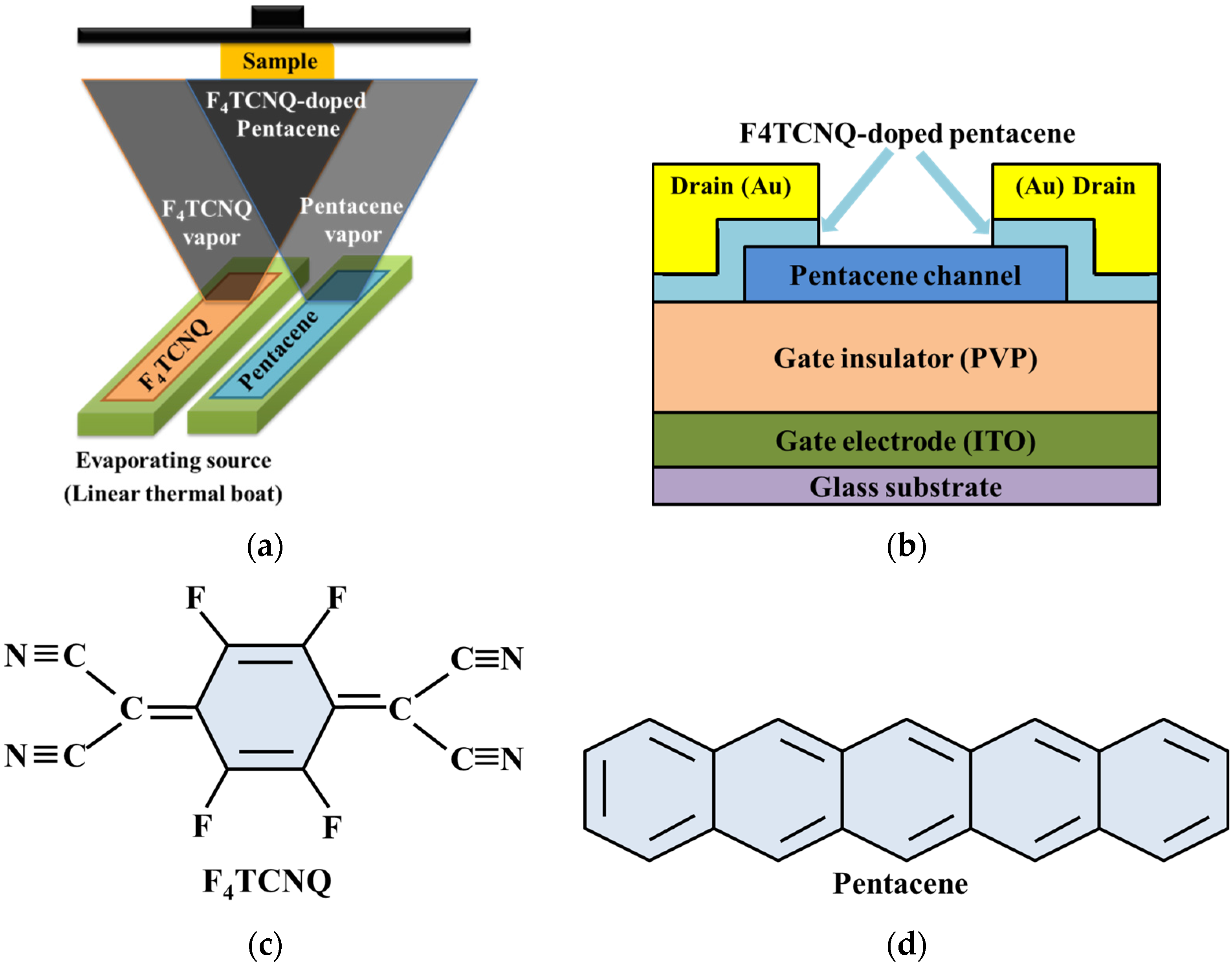
Pentacene-based OTFTs with a bottom-gate and top-contact structure were fabricated. A glass substrate with an indium-tin-oxide (ITO) layer was used as the substrate and as the bottom-gate electrode. A 350-nm-thick cross-linked poly (4-vinylphenol) (PVP) coating was provided on the ITO layer for use as the gate dielectric, and it was cured in a vacuum oven at 200 °C for 1.5 h. A 50-nm-thick pentacene channel layer was then deposited on the PVP layer through a shadow mask by using a thermal evaporator (base pressure: 2.0 × 10
−6 Torr) at a deposition rate of 0.2 Å/s and with the substrate temperature maintained at room temperature. Before the deposition of the S/D metal electrodes, a 1.5-nm-thick F
4TCNQ-doped pentacene carrier injection interlayer was deposited on the pentacene channel layer through a metal mask by simultaneously co-evaporating F
4TCNQ and pentacene from a thermal evaporator. In the co-evaporation process, the source materials of pentacene and F
4TCNQ were independently controlled, and were heated by linear thermal boat when the materials are deposited, as shown in
Figure 1a. The deposition rate of F
4TCNQ was fixed at 0.1 Å/s, while that of pentacene was set at 0.1, 0.3 and 1.0 Å/s; the designed F
4TCNQ:pentacene ratios corresponding to the pentacene deposition rates were 1:1, 1:3 and 1:10 respectively. Finally, Au (50 nm) S/D electrodes were formed through a shadow mask by using a thermal evaporator. Therefore, the F
4TCNQ-doped pentacene can be uniformly deposited to form the interlayer between pentacene channel layer and Au metal electrodes. The width and length of the electrode channels were 500 and 100 μm, respectively.
Figure 1b shows a schematic structure of the pentacene-based OTFTs with F
4TCNQ-doped pentacene interlayer, and
Figure 1c,d show the molecular structures of F
4TCNQ and pentacene, respectively. For convenience, the devices with F
4TCNQ:pentacene ratios of 1:1, 1:3 and 1:10 are hereafter designated as Devices 1, 2 and 3, respectively. A device without an F
4TCNQ-doped pentacene interlayer was considered the control sample. All measurements were performed under dark conditions and at an ambient temperature by using a semiconductor parameter analyzer (HP 4145B, HP Inc., Palo Alto, CA, USA).
Figure 1.
(a) a schematic diagram of the co-evaporation process; (b) a schematic structure of the pentacene-based organic thin-film transistors (OTFTs) with F4TCNQ-doped pentacene injection layer, and the molecular structures of (c) F4TCNQ and (d) pentacene, respectively.
Figure 1.
(a) a schematic diagram of the co-evaporation process; (b) a schematic structure of the pentacene-based organic thin-film transistors (OTFTs) with F4TCNQ-doped pentacene injection layer, and the molecular structures of (c) F4TCNQ and (d) pentacene, respectively.
3. Results and Discussion
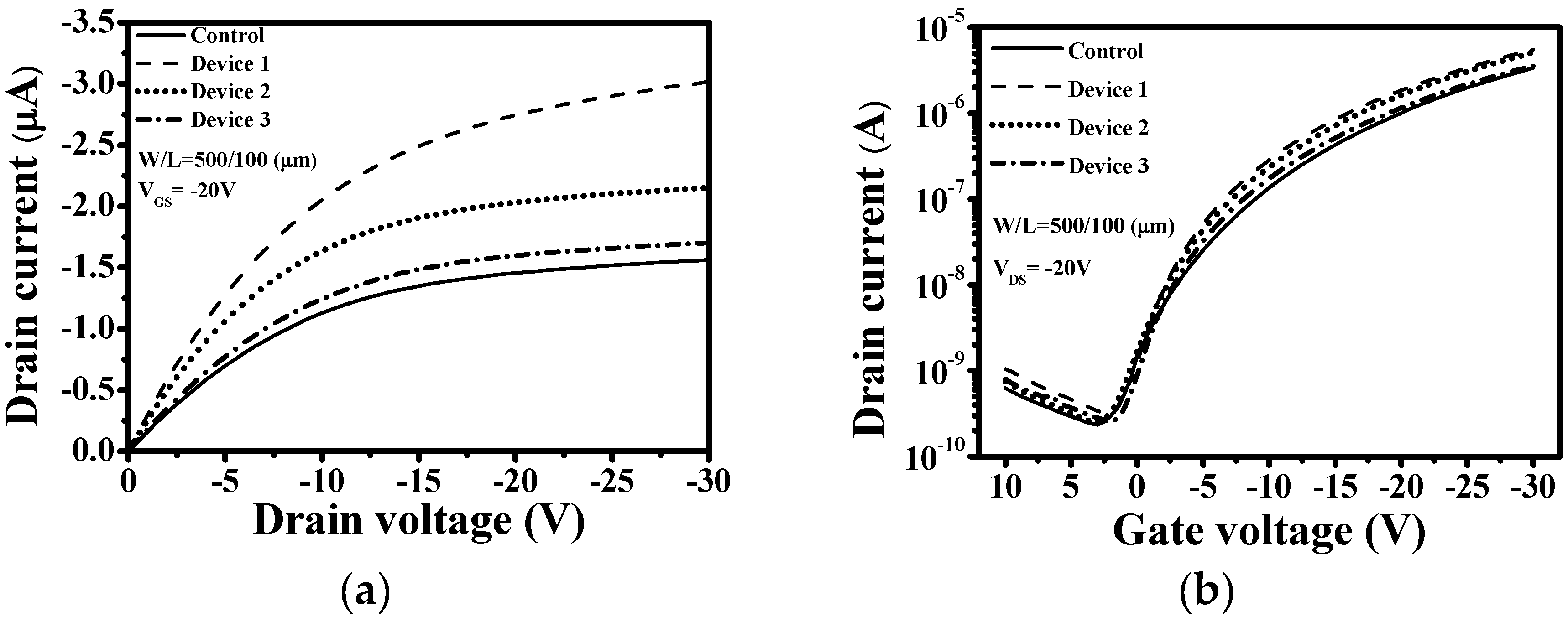
Figure 2a shows the output characteristics (
IDS-
VDS) of the devices with different F
4TCNQ:pentacene ratios for a
VGS = −20 V. The saturation current of Device 1 was −3.02 × 10
−6 A for
VDS and
VGS values of −30 and −20 V, respectively; this saturation current was much higher than those of Devices 2 and 3 and the control sample. The
IDS value of Device 1 was approximately 193% higher than that of the control sample.
Figure 2b shows the transfer characteristics (
IDS-
VGS) of the devices with different F
4TCNQ:pentacene ratios. The μ
FE value of Device 1 was enhanced by a factor of 1.6 and the on/off current ratio was enhanced by a factor of 1.5 compared with the control sample. This appreciable improvement in the electrical performance of Device 1 could be attributed to the F
4TCNQ:pentacene ratio being appropriate and to the charge density at interface between the S/D electrodes and the pentacene channel being high, improving charge injection [
12,
16]. However, the μ
FE value of the devices decreased with a decrease in the F
4TCNQ concentration of the F
4TCNQ-doped pentacene interlayer.
Figure 2.
Drain current characteristics of top-contact (TC) pentacene-based OTFTs with different F4TCNQ:pentacene ratios (Device 1 = 1:1, Device 2 = 1:3, and Device 3 = 1:10) (a) Output curves (IDS-VDS). (b) Transfer curves (IDS-VGS).
Figure 2.
Drain current characteristics of top-contact (TC) pentacene-based OTFTs with different F4TCNQ:pentacene ratios (Device 1 = 1:1, Device 2 = 1:3, and Device 3 = 1:10) (a) Output curves (IDS-VDS). (b) Transfer curves (IDS-VGS).
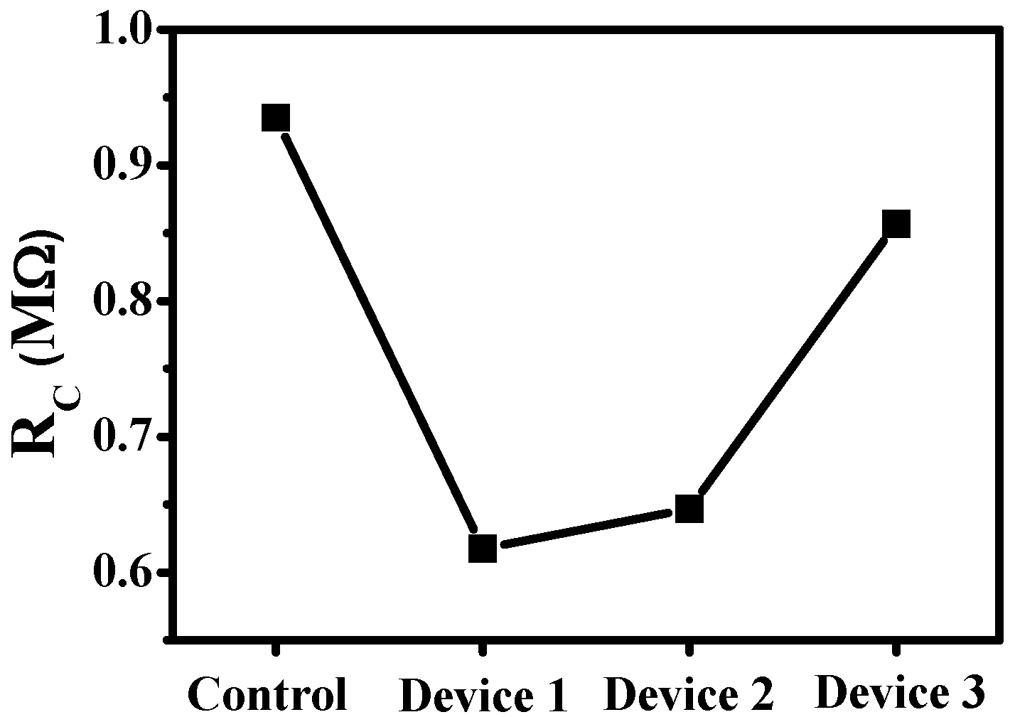
To quantitate the effect of the F
4TCNQ:pentacene ratio of the F
4TCNQ-doped pentacene interlayer on the electrical contact between the pentacene channel layer and the S/D metal electrodes, the channel length dependence of the total resistance (
RTotal) was determined according to the linear regions of the output characteristics of the fabricated devices. The channel lengths were 100, 150, 200 and 250 μm. The
RC value was obtained from the transmission line model (TLM) by extrapolating the
RTotal curve to obtain the
y-intercept for zero channel length [
17]. The
RC values of the four devices, determined from the TLM, are shown in
Figure 3. The
RC value of Device 1 at a gate voltage of −20 V was 0.617 × 10
6 Ω, which is approximately 1.5 times lower than that of the control sample (0.935 × 10
6 Ω). As shown in
Figure 3,
RC first decreases and then increases with a decrease in the F
4TCNQ concentration of the F
4TCNQ-doped pentacene interlayer. Apparently, the F
4TCNQ concentration affects hole transport across the interface between the S/D metal electrodes and the pentacene channel layer. In the presence of an F
4TCNQ-doped pentacene interlayer, the hole carrier could easily move through the F
4TCNQ-doped pentacene layer into the pentacene channel because of the improvement in the local conductivity and the formation of a multiple step barrier at the interlayer [
12,
16]. F
4TCNQ is an acceptor dopant, and therefore, in the interlayer, it leads to which hole doping involving the electron transfer of energy level between pentacene and F
4TCNQ, resulting in enhancing conductivity. Furthermore, the F
4TCNQ-doped pentacene interlayer changes the Fermi energy (
EF) position of the intrinsic pentacene, which leads to the formation of subdivided barriers instead of a single barrier in the interlayer, and enhances the injection of hole carriers from the Au electrodes to the pentacene channel. Consequently, the F
4TCNQ dopant amount can be easily fine-tuned to achieve the optimal device performance, which corresponds to a reduction in
RC, as shown in
Figure 3.
Figure 3.
The RC value as a function of F4TCNQ:pentacene ratio of TC pentacene-based OTFTs for VDS and VGS values of −2 and −20 V, respectively.
Figure 3.
The RC value as a function of F4TCNQ:pentacene ratio of TC pentacene-based OTFTs for VDS and VGS values of −2 and −20 V, respectively.
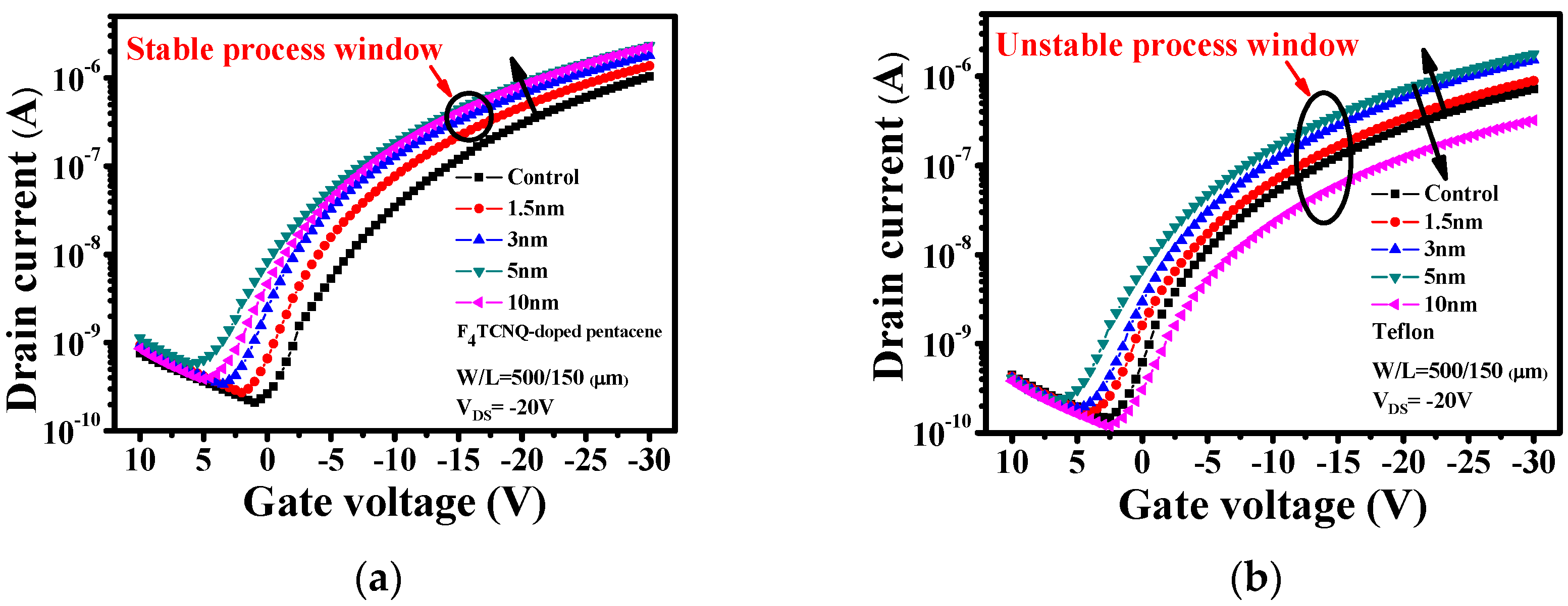
The dependence of the device performance on the thickness of the molecular-doping-type F
4TCNQ-doped pentacene layer was investigated. In a previous report of the present authors, the performance of pentacene-based OTFTs was found to be strongly dependent on the thickness of the insulating-type Teflon interlayer [
7]. To investigate the effect of the thickness of F
4TCNQ-doped pentacene and Teflon interlayers on the device performance, the F
4TCNQ:pentacene ratio of the F
4TCNQ-doped pentacene interlayer was fixed at 1:1, and the thicknesses of both carrier injection interlayers were set at 0, 1.5, 3, 5 and 10 nm.
Figure 4a,b shows the thickness-dependent transfer property of the device with Teflon and F
4TCNQ-doped pentacene interlayers of various thicknesses. The device with Teflon interlayer showed remarkable thickness dependence, while the one with F
4TCNQ-doped pentacene interlayer showed a slight dependence. In addition,
Figure 4c,d shows the AFM micrographs of the pentacene layers without and with a 5 nm F
4TCNQ-doped pentacene interlayer deposited on the PVP dielectric surface. The root mean square (rms) roughness for both devices without and with 5 nm F
4TCNQ-doped pentacene interlayer is 5.62 and 4.97 nm, respectively. It had been clearly seen that the surface become more smooth for devices with 5 nm F
4TCNQ-doped pentacene interlayer, which is necessary for providing a better contact with metal electrodes. This is the mechanism for lowering the barrier height and increasing the charge injection, and then improving device performance. The field-effect mobility (μ
FE) was calculated for a
VGS value of −30 V in the saturation region, and the threshold voltage (
VTH) was determined according to the saturation region of the plot of
|IDS|1/2 versus VGS [
18]. The sub-threshold swing (
SS) was calculated using the equation
SS =
dVGS/
d(log
10|IDS|). The maximum and minimum values of
IDS at a
VDS of −20 V were designated as
ION (on current) and
IOFF (off current), respectively [
19]. The thickness-dependent properties of pentacene-based OTFTs with Teflon and F
4TCNQ-doped pentacene interlayers of various thicknesses were summarized in
Table 1.
Figure 4.
Transfer characteristics of pentacene-based OTFTs with (a) F4TCNQ-doped pentacene and (b) Teflon interlayers of various thicknesses, and AFM images of pentacene films (c) without and (d) with 5 nm F4TCNQ-doped pentacene interlayer.
Figure 4.
Transfer characteristics of pentacene-based OTFTs with (a) F4TCNQ-doped pentacene and (b) Teflon interlayers of various thicknesses, and AFM images of pentacene films (c) without and (d) with 5 nm F4TCNQ-doped pentacene interlayer.
Table 1.
The electrical characteristics for the devices with F4TCNQ-doped pentacene and Teflon interlayers of various thicknesses.
Table 1.
The electrical characteristics for the devices with F4TCNQ-doped pentacene and Teflon interlayers of various thicknesses.
| Electrical Parameters | Molecular Doping Type: F4TCNQ-Doped Pentacene | Insulating Type: Teflon |
|---|
| Control | 1.5 nm | 3 nm | 5 nm | 10 nm | Control | 1.5 nm | 3 nm | 5 nm | 10 nm |
|---|
| VTH (V) | −7.7 | −5.7 | −4.4 | −4.1 | −4.2 | −6 | −5.9 | −5.5 | −3 | −5.3 |
| SS (V/decade) | 2.2 | 2.7 | 2.5 | 2.6 | 2.9 | 1.77 | 1.98 | 1.73 | 1.93 | 2.5 |
| μFE (cm2·V−1·s−1) | 0.12 | 0.14 | 0.17 | 0.21 | 0.2 | 0.08 | 0.09 | 0.12 | 0.15 | 0.02 |
| ION/IOFF (103) | 4.95 | 5 | 5.34 | 4.3 | 5.76 | 10.4 | 9.86 | 20.2 | 15.6 | 39.7 |
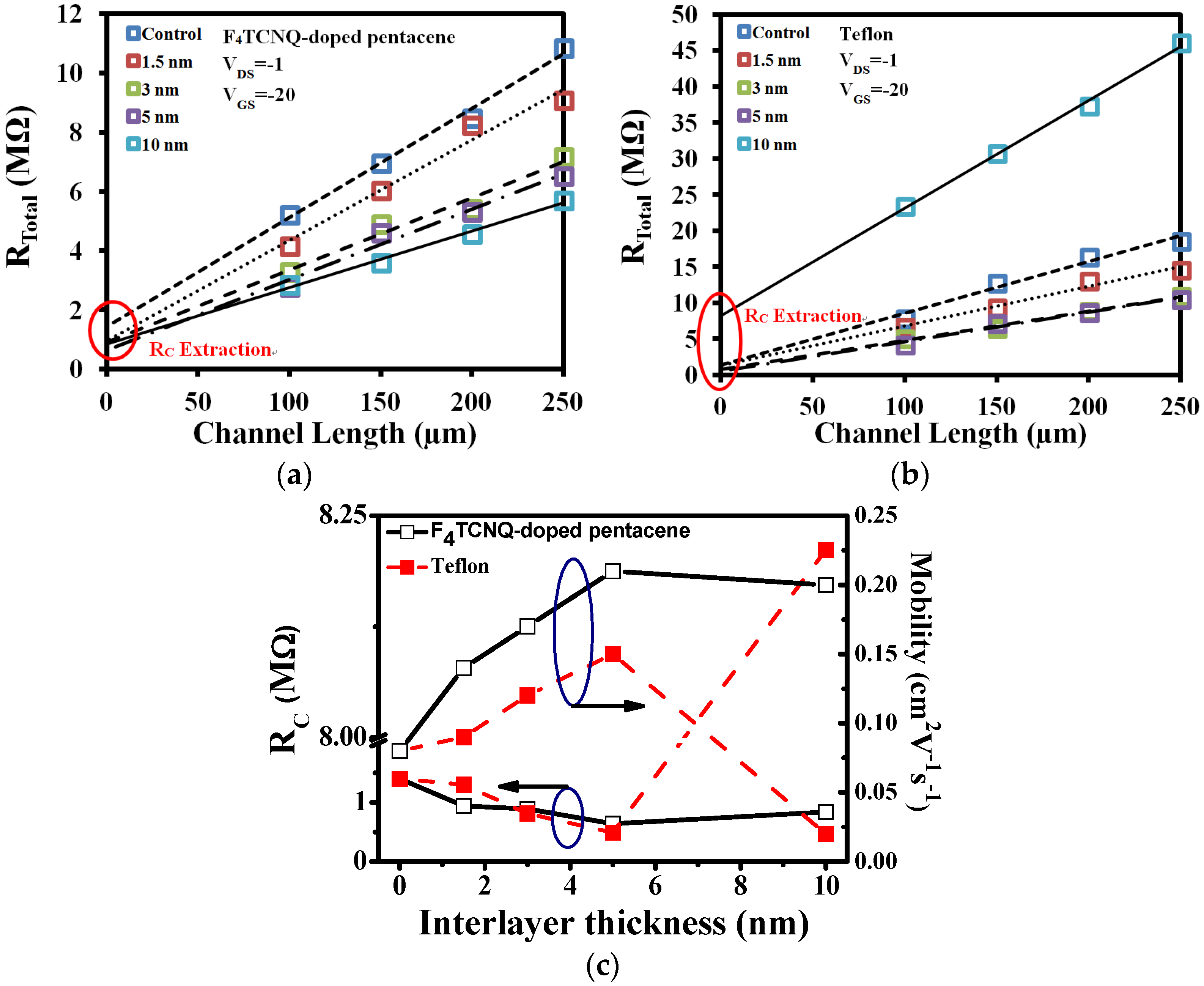
The
RTotal of the device with Teflon and F
4TCNQ-doped pentacene interlayers of various thicknesses is shown in
Figure 5a,b, respective. The variation of the
RC and μ
FE values with the carrier-injection interlayer thickness for the devices with Teflon and F
4TCNQ-doped pentacene interlayers is shown in
Figure 5c. The
RC value of the device with a molecular-doping-type F
4TCNQ-doped pentacene interlayer depended only slightly on the F
4TCNQ-doped pentacene interlayer thickness. The performances of both types of devices, according to μ
FE, increased with the thickness. However, when the interlayer thickness exceeded 5 nm, the μ
FE value of the device with an F
4TCNQ-doped pentacene interlayer decreased slightly; by contrast, the μ
FE value of the device with a Teflon interlayer decreased appreciably. It is presumed that the degradation of μ
FE can be directly attributed to the increase in
RC. Unlike the
RC value of the device with an insulating-type Teflon interlayer, the
RC value of the device with a molecular-doping-type F
4TCNQ-doped pentacene interlayer depended only slightly on the F
4TCNQ-doped pentacene interlayer thickness. Teflon is an insulating material with an extremely high resistivity (10
18 Ω·cm). Therefore, when the Teflon interlayer thickness exceeds a critical value, the insulating properties of the interlayer become dominant and reduce the carrier tunneling probability. Consequently, the device performance is degraded appreciably. It is to say that the molecular doping-type F
4TCNQ-doped pentacene interlayer is a suitable carrier injection layer that can not only improve the TC-OTFT performance but also facilitate obtaining a stable process window. It is the first time to compare the process windows for the interlayers of the insulating type and molecular-doping type. It is believed that the results will be interesting and important from the viewpoint of manufacturing as a result of the stable process window.
Figure 5.
The RTotal and RC of pentacene-based OTFTs with the different thickness of the (a) F4TCNQ-doped pentacene and (b) Teflon interlayer. (c) The variation of the mobility and Rc values with the various carrier-injection interlayer thickness for the devices with F4TCNQ-doped pentacene or Teflon interlayers.
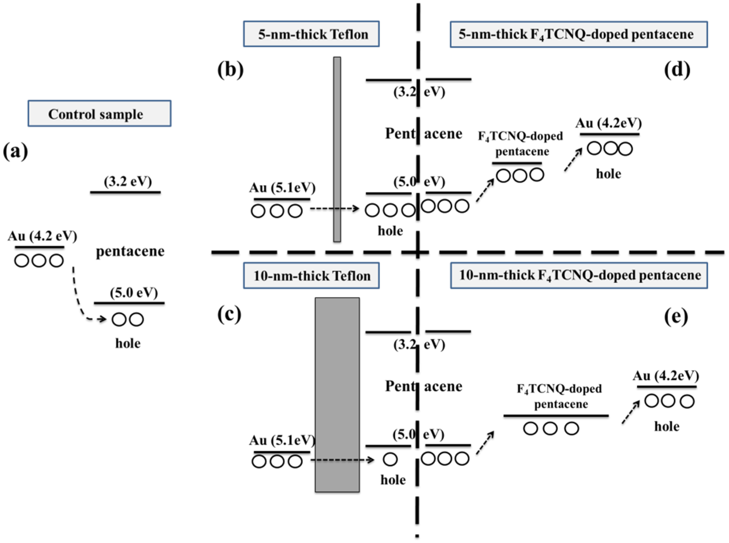
In
Figure 6, the dependence of the carrier injection efficiency on the thickness of the Teflon and F
4TCNQ-doped pentacene is clearly explained. In the control sample, hot Au atoms are directly deposited onto the pentacene channel layer, and diffuse into the upper layer of pentacene. A high energy barrier formed because of the presence of an interface dipole, there is a hole injection barrier of 0.8–1 eV between the Au electrodes and the pentacene channel layer, resulting in a relatively large hole injection barrier, as shown in
Figure 6a [
6,
7]. In addition, a high energy barrier associated with the formation of a metallic surface at the Au electrode/pentacene channel interface obstructed hole carrier transport. In the 5-nm-thick Teflon interlayer, the carriers could easily tunnel through to the pentacene channel layer because of suppressed metal penetration and a reduced hole injection barrier at the Au electrode/pentacene channel interface [
7]. However, for a Teflon layer thickness greater than 5 nm, the probability of carriers tunneling through clearly decreased because of the increased
RC at the Au electrode/pentacene channel interface. In the case of the F
4TCNQ-doped pentacene interlayer, regardless of its thickness (5- or 10-nm thick), the hole carriers could easily move through the interlayer to the Au electrodes because of the formation of a subdivided barrier and high local conductivity at the Au electrode/pentacene channel interface, which effectively reduced the hole injection barrier. Moreover, in the device containing a 5-nm-thick F
4TCNQ-doped pentacene interlayer with an F
4TCNQ:pentacene ratio of 1:1, the carrier injection efficiency is high and
RC is low, resulting in high device performance. Even when the thickness of the F
4TCNQ-doped pentacene interlayer was 10 nm, the effect of the thickness on the OTFT electrical performance was not apparent, implying that the thickness dependence of the electrical performance of OTFTs with a molecular-doping-type F
4TCNQ-doped pentacene interlayer is weaker than that of the performance of OTFTs with an insulating-type Teflon interlayer. Therefore, it is believed that an F
4TCNQ-doped pentacene interlayer is a good candidate as a carrier injection layer for TC pentacene-based OTFTs since it provides a high carrier injection efficiency and a stable process window.
Figure 6.
Band diagram of top-contact (TC) pentacene-based OTFTs with various interlayer thicknesses (a) control sample, (b) 5-, and (c) 10-nm-thick Teflon and (d) 5-, and (e) 10-nm-thick F4TCNQ-doped pentacene.
Figure 6.
Band diagram of top-contact (TC) pentacene-based OTFTs with various interlayer thicknesses (a) control sample, (b) 5-, and (c) 10-nm-thick Teflon and (d) 5-, and (e) 10-nm-thick F4TCNQ-doped pentacene.


